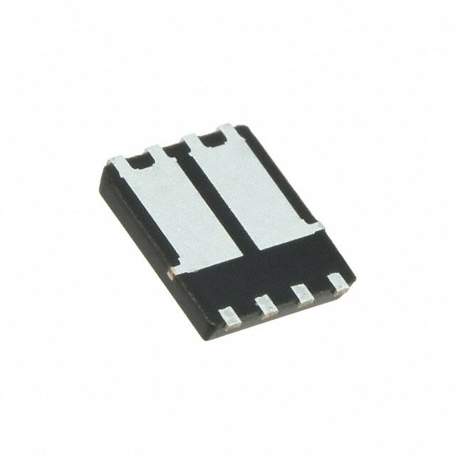
BSC072N04LD
MOSFET
OptiMOSTM-T2�Power�Transistor,�40�V
PG-TDSON-8-4
8
Features
·�Dual�N-channel,�logic�level
·�Fast�switching�MOSFETs�for�SMPS
·�Optimized�technology�for�Synchronous�Rectification
·�Pb-free�plating;�RoHS�compliant
·�100%�Avalanche�tested
·�Halogen-free�according�to�IEC61249-2-21
·�Superior�thermal�resistance
Product�Validation
Qualified�for�industrial�applications�according�to�the�relevant�tests�of
JEDEC47/20/22
1
2
7
1
6
8
3
2
5
7
6
4
3
4
5
D1 D1
D2 D2
S1
S2
Table�1�����Key�Performance�Parameters
Parameter
Value
Unit
VDS
40
V
RDS(on),max
7.2
mΩ
ID
20
A
Type�/�Ordering�Code
Package
BSC072N04LD
SSO8 dual (TDSON-8-4)
Final Data Sheet
Marking
072N04LD
1
G1
G2
Related�Links
-
Rev.�2.0,��2018-12-11
�OptiMOSTM-T2�Power�Transistor,�40�V
BSC072N04LD
Table�of�Contents
Description . . . . . . . . . . . . . . . . . . . . . . . . . . . . . . . . . . . . . . . . . . . . . . . . . . . . . . . . . . . . . . . . . . . . . . . . . . . . . 1
Maximum ratings . . . . . . . . . . . . . . . . . . . . . . . . . . . . . . . . . . . . . . . . . . . . . . . . . . . . . . . . . . . . . . . . . . . . . . . . 3
Thermal characteristics . . . . . . . . . . . . . . . . . . . . . . . . . . . . . . . . . . . . . . . . . . . . . . . . . . . . . . . . . . . . . . . . . . . . 3
Electrical characteristics . . . . . . . . . . . . . . . . . . . . . . . . . . . . . . . . . . . . . . . . . . . . . . . . . . . . . . . . . . . . . . . . . . . 3
Electrical characteristics diagrams . . . . . . . . . . . . . . . . . . . . . . . . . . . . . . . . . . . . . . . . . . . . . . . . . . . . . . . . . . . 5
Package Outlines . . . . . . . . . . . . . . . . . . . . . . . . . . . . . . . . . . . . . . . . . . . . . . . . . . . . . . . . . . . . . . . . . . . . . . . . 9
Revision History . . . . . . . . . . . . . . . . . . . . . . . . . . . . . . . . . . . . . . . . . . . . . . . . . . . . . . . . . . . . . . . . . . . . . . . . 10
Trademarks . . . . . . . . . . . . . . . . . . . . . . . . . . . . . . . . . . . . . . . . . . . . . . . . . . . . . . . . . . . . . . . . . . . . . . . . . . . 10
Disclaimer . . . . . . . . . . . . . . . . . . . . . . . . . . . . . . . . . . . . . . . . . . . . . . . . . . . . . . . . . . . . . . . . . . . . . . . . . . . . 10
Final Data Sheet
2
Rev.�2.0,��2018-12-11
�OptiMOSTM-T2�Power�Transistor,�40�V
BSC072N04LD
1�����Maximum�ratings
at�TA=25�°C,�unless�otherwise�specified,�one�transistor�active
Table�2�����Maximum�ratings
Parameter
Symbol
Continuous drain current
Values
Unit
Note�/�Test�Condition
20
A
VGS=10�V,�TC=25�°C
-
80
A
TA=25�°C
-
-
87
mJ
ID=10�A,�RGS=25�Ω
VGS
-16
-
16
V
-
Power dissipation
Ptot
-
-
65
W
TC=25�°C
Operating and storage temperature
Tj,�Tstg
-55
-
175
°C
IEC climatic category; DIN IEC 68-1:
55/175/56
Unit
Note�/�Test�Condition
Min.
Typ.
Max.
ID
-
-
ID,pulse
-
Avalanche energy, single pulse
EAS
Gate source voltage
Pulsed drain current1)
2)
2�����Thermal�characteristics
Table�3�����Thermal�characteristics
Parameter
Symbol
Thermal resistance, junction - case,
bottom
Values
Min.
Typ.
Max.
RthJC
-
-
2.3
°C/W -
Device on PCB,
6 cm² cooling area3)
RthJA
-
-
60
°C/W -
Device on PCB,
minimal footprint4)
RthJA
-
-
100
°C/W -
3�����Electrical�characteristics
at�Tj=25�°C,�unless�otherwise�specified
Table�4�����Static�characteristics
Parameter
Symbol
Drain-source breakdown voltage
Values
Unit
Note�/�Test�Condition
-
V
VGS=0�V,�ID=1�mA
1.7
2.2
V
VDS=VGS,�ID=30�µA
-
0.1
10
1
100
µA
VDS=40�V,�VGS=0�V,�Tj=25�°C
VDS=40�V,�VGS=0�V,�Tj=125�°C
IGSS
-
-
100
nA
VGS=20�V,�VDS=0�V
RDS(on)
-
6.5
8.0
7.2
9.2
mΩ
VGS=10�V,�ID=17�A
VGS=4.5�V,�ID=10�A
Min.
Typ.
Max.
V(BR)DSS
40
-
Gate threshold voltage
VGS(th)
1.2
Zero gate voltage drain current
IDSS
Gate-source leakage current
Drain-source on-state resistance
1)
See Diagram 3 for more detailed information
See Diagram 13 for more detailed information
3)
Device on 40 mm x 40 mm x 1.5 mm epoxy PCB FR4 with 6 cm2 (one layer, 70 µm thick) copper area for drain connection.
PCB is vertical in still air.
4)
device mounted on a minimum pad (one layer, 70 µm thick)
2)
Final Data Sheet
3
Rev.�2.0,��2018-12-11
�OptiMOSTM-T2�Power�Transistor,�40�V
BSC072N04LD
Table�5�����Dynamic�characteristics
Parameter
Symbol
Values
Unit
Note�/�Test�Condition
3990
pF
VGS=0�V,�VDS=20�V,�f=1�MHz
680
880
pF
VGS=0�V,�VDS=20�V,�f=1�MHz
-
36
72
pF
VGS=0�V,�VDS=20�V,�f=1�MHz
td(on)
-
9
-
ns
VDD=20�V,�VGS=10�V,�ID=20�A,
RG,ext=11�Ω
Rise time
tr
-
4
-
ns
VDD=20�V,�VGS=10�V,�ID=20�A,
RG,ext=11�Ω
Turn-off delay time
td(off)
-
50
-
ns
VDD=20�V,�VGS=10�V,�ID=20�A,
RG,ext=11�Ω
Fall time
tf
-
25
-
ns
VDD=20�V,�VGS=10�V,�ID=20�A,
RG,ext=11�Ω
Unit
Note�/�Test�Condition
Min.
Typ.
Max.
Ciss
-
3070
Output capacitance
Coss
-
Reverse transfer capacitance1)
Crss
Turn-on delay time
Input capacitance1)
1)
Table�6�����Gate�charge�characteristics2)�
Parameter
Symbol
Gate to source charge
Values
Min.
Typ.
Max.
Qgs
-
9
13
nC
VDD=20�V,�ID=20�A,�VGS=0�to�10�V
Gate to drain charge
Qgd
-
4.1
8.2
nC
VDD=20�V,�ID=20�A,�VGS=0�to�10�V
Gate charge total1)
Qg
-
39
52
nC
VDD=20�V,�ID=20�A,�VGS=0�to�10�V
Gate plateau voltage
Vplateau
-
3.1
-
V
VDD=20�V,�ID=20�A,�VGS=0�to�10�V
Unit
Note�/�Test�Condition
Table�7�����Reverse�diode
Parameter
Symbol
Diode continuous forward current
Values
Min.
Typ.
Max.
IS
-
-
20
A
TC=25�°C
Diode pulse current
IS,pulse
-
-
80
A
TC=25�°C
Diode forward voltage
VSD
-
0.85
1.1
V
VGS=0�V,�IF=17�A,�Tj=25�°C
trr
-
35
-
ns
VR=15�V,�IF=9�A,�diF/dt=100�A/µs
Qrr
-
35
-
nC
VR=15�V,�IF=9�A,�diF/dt=100�A/µs
Reverse recovery time1)
1)
Reverse recovery charge
1)
2)
Defined by design. Not subject to production test.
See ″Gate charge waveforms″ for parameter definition
Final Data Sheet
4
Rev.�2.0,��2018-12-11
�OptiMOSTM-T2�Power�Transistor,�40�V
BSC072N04LD
4�����Electrical�characteristics�diagrams
Diagram�1:�Power�dissipation
Diagram�2:�Drain�current
70
80
60
70 silicon limit
60
50
ID�[A]
Ptot�[W]
50
40
40
30
30
20
20 package limit
10
0
10
0
25
50
75
100
125
150
175
0
200
0
25
50
75
TA�[°C]
100
125
150
175
200
TA�[°C]
Ptot=f(TA),�minimal�footprint
ID=f(TA);�minimal�footprint
Diagram�3:�Safe�operating�area
Diagram�4:�Max.�transient�thermal�impedance
2
101
10
single pulse
0.01
0.02
0.05
0.1
0.2
0.5
1 µs
10 µs
10 ms
100 µs
DC
1 ms
100
ID�[A]
ZthJC�[K/W]
101
100
10-1
10-1
10-1
100
101
102
10-2
10-5
10-4
VDS�[V]
10-2
10-1
100
tp�[s]
ID=f(VDS);�TC=25�°C;�D=0;�parameter:�tp
Final Data Sheet
10-3
ZthJC=f(tp);�parameter:�D=tp/T
5
Rev.�2.0,��2018-12-11
�OptiMOSTM-T2�Power�Transistor,�40�V
BSC072N04LD
Diagram�5:�Typ.�output�characteristics
80
Diagram�6:�Typ.�drain-source�on�resistance
40
4V
3.5 V
70
10 V
4.5 V
30
ID�[A]
50
3.5 V
40
30
RDS(on)��[mΩ]
60
20
4V
3V
20
10
4.5 V
3V
10 V
10
0
0.0
1.0
2.0
3.0
0
4.0
0
10
20
30
VDS�[V]
40
50
60
ID=f(VDS),�Tj=25�°C;�parameter:�VGS
RDS(on)=f(ID),�Tj=25�°C;�parameter:�VGS
Diagram�7:�Typ.�transfer�characteristics
Diagram�8:�Typ.�drain-source�on�resistance
80
20.0
70
17.5
60
15.0
50
12.5
RDS(on)��[mΩ]
ID�[A]
70
80
ID�[A]
40
30
20
175 °C
10.0
7.5
25 °C
5.0
175 °C
10
0
2.5
25 °C
0
1
2
3
4
5
VGS�[V]
0
2
4
6
8
10
VGS�[V]
ID=f(VGS),�|VDS|>2|ID|RDS(on)max;�parameter:�Tj
Final Data Sheet
0.0
RDS(on)=f(VGS),�ID=17�A;�parameter:�Tj
6
Rev.�2.0,��2018-12-11
�OptiMOSTM-T2�Power�Transistor,�40�V
BSC072N04LD
Diagram�9:�Normalized�drain-source�on�resistance
Diagram�10:�Typ.�gate�threshold�voltage
1.75
2.00
1.75
1.50
1.25
1.25
1.00
VGS(th)�[V]
RDS(on)�(normalized�to�25�°C)
1.50
0.75
1.00
300 µA
0.75
0.50
30 µA
0.50
0.25
0.25
0.00
-80
-40
0
40
80
120
160
0.00
-80
200
-40
0
40
Tj�[°C]
80
120
160
RDS(on)=f(Tj),�ID=17�A,�VGS=10�V
VGS(th=f(Tj),�VGS=VDS;�parameter:�ID
Diagram�11:�Typ.�capacitances
Diagram�12:�Forward�characteristics�of�reverse�diode
4
102
10
25 °C
25 °C, max
175 °C
175 °C, max
Ciss
Coss
102
IF�[A]
101
C�[pF]
103
101
200
Tj�[°C]
100
Crss
0
5
10
15
20
25
30
35
40
10-1
0.00
0.25
VDS�[V]
0.75
1.00
1.25
1.50
VSD�[V]
C=f(VDS);�VGS=0�V;�f=1�MHz
Final Data Sheet
0.50
IF=f(VSD);�parameter:�Tj
7
Rev.�2.0,��2018-12-11
�OptiMOSTM-T2�Power�Transistor,�40�V
BSC072N04LD
Diagram�13:�Avalanche�characteristics
Diagram�14:�Typ.�gate�charge
2
10
10
8V
20 V
32 V
8
101
6
IAV�[A]
VGS�[V]
25 °C
100 °C
4
150 °C
2
0
10
10-1
100
101
102
103
tAV�[µs]
0
0
5
10
15
20
25
30
35
40
Qgate�[nC]
IAS=f(tAV);�RGS=25�Ω;�parameter:�Tj,start
VGS=f(Qgate),�ID=20�A�pulsed,�Tj=25�°C;�parameter:�VDD
Diagram�15:�Drain-source�breakdown�voltage
Diagram Gate charge waveforms
44
43
VBR(DSS)�[V]
42
41
40
39
38
-80
-40
0
40
80
120
160
200
Tj�[°C]
VBR(DSS)=f(Tj);�ID=1�mA
Final Data Sheet
8
Rev.�2.0,��2018-12-11
�OptiMOSTM-T2�Power�Transistor,�40�V
BSC072N04LD
5�����Package�Outlines
DIMENSIONS
A
A1
b
b1
D
D1
D2
E
E1
E2
E3
E4
e
L
M
Θ
aaa
ddd
MILLIMETERS
MIN.
MAX.
0.90
1.10
0.15
0.35
0.34
0.54
0.02
0.22
4.95
5.35
4.20
4.40
0.50
0.70
5.95
6.35
5.70
6.10
4.075
4.275
4.035
4.235
0.15
0.35
1.27
0.45
0.65
0.45
0.65
8.5°
11.5°
0.05
0.10
DOCUMENT NO.
Z8B00189767
REVISION
01
SCALE 5:1
0
1
2
3
4mm
EUROPEAN PROJECTION
ISSUE DATE
31.07.2018
Figure�1�����Outline�SSO8�dual�(TDSON-8-4),�dimensions�in�mm
Final Data Sheet
9
Rev.�2.0,��2018-12-11
�OptiMOSTM-T2�Power�Transistor,�40�V
BSC072N04LD
Revision�History
BSC072N04LD
Revision:�2018-12-11,�Rev.�2.0
Previous Revision
Revision
Date
Subjects (major changes since last revision)
2.0
2018-12-11
Release of final version
Trademarks
All�referenced�product�or�service�names�and�trademarks�are�the�property�of�their�respective�owners.
We�Listen�to�Your�Comments
Any�information�within�this�document�that�you�feel�is�wrong,�unclear�or�missing�at�all?�Your�feedback�will�help�us�to�continuously
improve�the�quality�of�this�document.�Please�send�your�proposal�(including�a�reference�to�this�document)�to:
erratum@infineon.com
Published�by
Infineon�Technologies�AG
81726�München,�Germany
©�2018�Infineon�Technologies�AG
All�Rights�Reserved.
Legal�Disclaimer
The�information�given�in�this�document�shall�in�no�event�be�regarded�as�a�guarantee�of�conditions�or�characteristics�
(“Beschaffenheitsgarantie”)�.
With�respect�to�any�examples,�hints�or�any�typical�values�stated�herein�and/or�any�information�regarding�the�application�of�the
product,�Infineon�Technologies�hereby�disclaims�any�and�all�warranties�and�liabilities�of�any�kind,�including�without�limitation
warranties�of�non-infringement�of�intellectual�property�rights�of�any�third�party.
In�addition,�any�information�given�in�this�document�is�subject�to�customer’s�compliance�with�its�obligations�stated�in�this
document�and�any�applicable�legal�requirements,�norms�and�standards�concerning�customer’s�products�and�any�use�of�the
product�of�Infineon�Technologies�in�customer’s�applications.
The�data�contained�in�this�document�is�exclusively�intended�for�technically�trained�staff.�It�is�the�responsibility�of�customer’s
technical�departments�to�evaluate�the�suitability�of�the�product�for�the�intended�application�and�the�completeness�of�the�product
information�given�in�this�document�with�respect�to�such�application.
Information
For�further�information�on�technology,�delivery�terms�and�conditions�and�prices�please�contact�your�nearest�Infineon
Technologies�Office�(www.infineon.com).
Warnings
Due�to�technical�requirements,�components�may�contain�dangerous�substances.�For�information�on�the�types�in�question,
please�contact�the�nearest�Infineon�Technologies�Office.
The�Infineon�Technologies�component�described�in�this�Data�Sheet�may�be�used�in�life-support�devices�or�systems�and/or
automotive,�aviation�and�aerospace�applications�or�systems�only�with�the�express�written�approval�of�Infineon�Technologies,�if�a
failure�of�such�components�can�reasonably�be�expected�to�cause�the�failure�of�that�life-support,�automotive,�aviation�and
aerospace�device�or�system�or�to�affect�the�safety�or�effectiveness�of�that�device�or�system.�Life�support�devices�or�systems�are
intended�to�be�implanted�in�the�human�body�or�to�support�and/or�maintain�and�sustain�and/or�protect�human�life.�If�they�fail,�it�is
reasonable�to�assume�that�the�health�of�the�user�or�other�persons�may�be�endangered.
Final Data Sheet
10
Rev.�2.0,��2018-12-11
�