B TC5 00 1 0 -1 TA A & B TC3 0 01 0 - 1T A A
Smart High-Side Power Connector
2x Single Channel, 2x 1m
D at a S h e et
1.3, 2015-02-06
A u t om o t iv e Po w er
�BTC50010-1TAA & BTC30010-1TAA
Table of Contents
Table of Contents . . . . . . . . . . . . . . . . . . . . . . . . . . . . . . . . . . . . . . . . . . . . . . . . . . . . . . . . . . . . . . . . 2
1
Overview . . . . . . . . . . . . . . . . . . . . . . . . . . . . . . . . . . . . . . . . . . . . . . . . . . . . . . . . . . . . . . . . . . . . . . . 3
2
Block Diagram . . . . . . . . . . . . . . . . . . . . . . . . . . . . . . . . . . . . . . . . . . . . . . . . . . . . . . . . . . . . . . . . . . . 5
3
3.1
3.2
3.3
Pin Configuration . . . . . . . . . . . . . . . . . . . . . . . . . . . . . . . . . . . . . . . . . . . . . . . . . . . . . . . . . . . . . . . .
Pin Assignment . . . . . . . . . . . . . . . . . . . . . . . . . . . . . . . . . . . . . . . . . . . . . . . . . . . . . . . . . . . . . . . . . . .
Pin Definitions and Functions . . . . . . . . . . . . . . . . . . . . . . . . . . . . . . . . . . . . . . . . . . . . . . . . . . . . . . . .
Voltage and Current Definition . . . . . . . . . . . . . . . . . . . . . . . . . . . . . . . . . . . . . . . . . . . . . . . . . . . . . . .
4
4.1
4.2
4.3
General Product Characteristics . . . . . . . . . . . . . . . . . . . . . . . . . . . . . . . . . . . . . . . . . . . . . . . . . . . . 9
Absolute Maximum Ratings . . . . . . . . . . . . . . . . . . . . . . . . . . . . . . . . . . . . . . . . . . . . . . . . . . . . . . . . . 9
Functional Range . . . . . . . . . . . . . . . . . . . . . . . . . . . . . . . . . . . . . . . . . . . . . . . . . . . . . . . . . . . . . . . . 12
Thermal Resistance . . . . . . . . . . . . . . . . . . . . . . . . . . . . . . . . . . . . . . . . . . . . . . . . . . . . . . . . . . . . . . 14
5
5.1
5.1.1
5.1.2
5.2
5.3
5.4
5.5
5.6
5.7
5.8
Functional Description . . . . . . . . . . . . . . . . . . . . . . . . . . . . . . . . . . . . . . . . . . . . . . . . . . . . . . . . . . .
Power Stage . . . . . . . . . . . . . . . . . . . . . . . . . . . . . . . . . . . . . . . . . . . . . . . . . . . . . . . . . . . . . . . . . . . .
Output ON-State Resistance . . . . . . . . . . . . . . . . . . . . . . . . . . . . . . . . . . . . . . . . . . . . . . . . . . . . . .
Switching an Inductive Load . . . . . . . . . . . . . . . . . . . . . . . . . . . . . . . . . . . . . . . . . . . . . . . . . . . . . .
Gate Driver Functionality . . . . . . . . . . . . . . . . . . . . . . . . . . . . . . . . . . . . . . . . . . . . . . . . . . . . . . . . . .
Undervoltage Protection . . . . . . . . . . . . . . . . . . . . . . . . . . . . . . . . . . . . . . . . . . . . . . . . . . . . . . . . . . .
Overvoltage Protection . . . . . . . . . . . . . . . . . . . . . . . . . . . . . . . . . . . . . . . . . . . . . . . . . . . . . . . . . . . .
Protection during Loss of Load or Loss of VS Condition . . . . . . . . . . . . . . . . . . . . . . . . . . . . . . . . . . .
BTC50010-1TAA Inverse Current Capability . . . . . . . . . . . . . . . . . . . . . . . . . . . . . . . . . . . . . . . . . . .
Reverse Polarity Protection . . . . . . . . . . . . . . . . . . . . . . . . . . . . . . . . . . . . . . . . . . . . . . . . . . . . . . . .
Electrical Characteristics . . . . . . . . . . . . . . . . . . . . . . . . . . . . . . . . . . . . . . . . . . . . . . . . . . . . . . . . . .
15
15
15
15
17
18
19
19
20
21
22
6
6.1
6.2
6.3
Application Information . . . . . . . . . . . . . . . . . . . . . . . . . . . . . . . . . . . . . . . . . . . . . . . . . . . . . . . . . .
Information for Application Combining PWM Mode with Fuse . . . . . . . . . . . . . . . . . . . . . . . . . . . . . .
Information for Driving Capability of Charge Pump Pin after Switch ON . . . . . . . . . . . . . . . . . . . . . .
Further Application Information . . . . . . . . . . . . . . . . . . . . . . . . . . . . . . . . . . . . . . . . . . . . . . . . . . . . . .
29
31
32
32
7
Package Outlines . . . . . . . . . . . . . . . . . . . . . . . . . . . . . . . . . . . . . . . . . . . . . . . . . . . . . . . . . . . . . . . 33
8
Revision History . . . . . . . . . . . . . . . . . . . . . . . . . . . . . . . . . . . . . . . . . . . . . . . . . . . . . . . . . . . . . . . . 34
Data Sheet
Connect FET & Companion
2
6
6
6
8
1.3, 2015-02-06
�High-Side Power Connector
1
BTC50010-1TAA &
BTC30010-1TAA
Overview
Applications
Switching resistive, capacitive and inductive loads in conjunction with
an effective peripheral free wheeling circuit
Replaces electromechanical relay
Most suitable for high current applications, such as Start-Stop, power
distribution, main switch, heating systems
PWM application with low frequencies
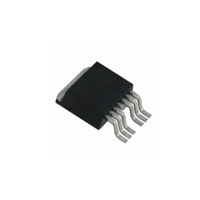
PG-TO-263-7-8
Features
Load or Supply Line switching up to 60 A DC
Operating temperature up to 150°C
Current controlled Input pin
Low Stand-by current
Two times one channel device, easily be combined for reverse blocking or to halve the RDS(ON)
Electrostatic discharge protected (ESD)
Optimized Electromagnetic Compatibility (EMC)
Very low power consumption in ON state
Compatible to cranking pulse requirement (test pulse 4 in ISO7637 and cold start pulse in LV124)
Infineon® Reversave: Reverse battery protection by self turn ON of the power MOSFET
Inverse operation robustness capability
Infineon® SMART CLAMPING
Green Product (RoHS compliant, halogen free package)
AEC Qualified
Dustproof
Description
The BTC50010-1TAA & BTC30010-1TAA are one High-Side Power Connector (BTC50010-1TAA) combined with
a perfect fitting n-channel MOSFET (BTC30010-1TAA) to replace electromechanical relay. These easy to use twin
devices can provide higher current-driven capability or additional reverse polarity protection feature. They offer
switching without audible noise, weight reduction and increased switching cycle capability to comply with
upcoming requirements on power distribution applications (e.g. battery disconnect switch). In addition, they
Type
Package
Marking
BTC50010-1TAA
PG-TO-263-7-8
C50010A
BTC30010-1TAA
PG-TO-263-7-8
C30010A
Data Sheet
Connect FET & Companion
3
1.3, 2015-02-06
�BTC50010-1TAA & BTC30010-1TAA
Overview
significantly reduce power/current consumption of the device while ON to increase energy efficiency. The device
can withstand harshest cranking pulse such as test pulse 4 in ISO7637 and cold start pulse in LV124.
Table 1
Product Summary
Parameter
Symbol
Values
Weight (approx.)
G1
1.5 g
Nominal operating voltage
VS(OP)
8 V
18 V
Extended operating voltage contain dynamic undervoltage capability
VS(DYN)
3.2 V
28 V
Nominal load current
IL(NOM)
30 A
Typical ON-state resistance at TJ = 25 °C (CP pin open)
RDS(ON)
0.9 m
Typical input current in ON state
IIN(ON)
2 mA
Typical stand-by current at TJ = 25 °C
IS(OFF)
3 µA
Weight (approx.)
G2
1.5 g
Nominal load current
IL(NOM)_C
30 A
Typical ON-state resistance at TJ = 25 °C
RDS(ON)
0.9 m
Operating voltage
VS(OP)
8 V
18 V
Extended operating voltage contain dynamic undervoltage capability
VS(DYN)
3.2 V
28 V
Nominal load current of parallel connected BTC50010-1TAA &
BTC30010-1TAA
IL(NOM) + IL(NOM)_C 60 A
BTC50010-1TAA
BTC30010-1TAA
BTC50010-1TAA & BTC30010-1TAA
Data Sheet
Connect FET & Companion
4
1.3, 2015-02-06
�BTC50010-1TAA & BTC30010-1TAA
Block Diagram
2
Block Diagram
Internal
Power
Supply
R VS
(AZ )I N
ON Mode
Control
IN1
Driver
Logic
IN2
VS
Smart
Clamp
Gate Control
&
Charge
Pump
OUT
ESD
Protection
V Z = 6V
CP
Figure 1
Block Diagram BTC50010-1TAA
Drain
Smart
Clamp
Gate
ESD
Protection
Source
Figure 2
Block Diagram BTC30010-1TAA
Data Sheet
Connect FET & Companion
5
1.3, 2015-02-06
�BTC50010-1TAA & BTC30010-1TAA
Pin Configuration
3
Pin Configuration
3.1
Pin Assignment
4
1 2 3
5 6 7
Figure 3
Pin Configuration for BTC50010-1TAA and BTC30010-1TAA
3.2
Pin Definitions and Functions
Table 2
Pin definition and functions of BTC50010-1TAA
Pin
Symbol
Function
1
IN1
IN; Pull down to module ground for channel activation 1)
2
IN2
IN2; Pull down to module ground for channel activation1)
3
CP
Charge Pump Output; Output pin of internal charge pump voltage of BTC500101TAA for driving BTC30010-1TAA
4, Cooling Tab VS
Supply Voltage; Connected to battery voltage
5, 6, 7
OUTPUT; High side power output2)
OUT
1) IN1 and IN2 are internally connected
2) All output pins are connected internally. All output pins have to be connected externally together on PCB. Not shorting all
outputs pins will considerably increase the ON-resistance. PCB traces have to be designed to withstand the maximum
current which can flow. PCB traces for output current are recommended to be designed symmetrically or having similar
line resistance for any of the three output pins from this device.
Data Sheet
Connect FET & Companion
6
1.3, 2015-02-06
�BTC50010-1TAA & BTC30010-1TAA
Pin Configuration
Table 3
Pin definitions and functions of BTC30010-1TAA
Pin
Symbol
Function
1
Gate
Gate; is not allowed to be floating and has to be connected to CP pin of BTC500101TAA to be switched ON/OFF by BTC50010-1TAA.
2
NC
3
NC
4, Cooling Tab Drain
Drain; Connected to battery voltage for Parallel Circuit to halve the RDS(ON)
application in Figure 27. Connected to load for Blocking Current in Reverse
Polarity application in Figure 28.
5, 6, 7
Source; N-channel MOSFET Source1). Connected to BTC50010-1TAA OUT pin
for Parallel Circuit to halve the RDS(ON) application in Figure 27. Connected to
BTC50010-1TAA OUT pin for Blocking Current in Reverse Polarity application in
Figure 28.
Source
1) All Source pins are connected internally. All Source pins have to be connected externally together on PCB. Not shorting all
outputs pins will considerably increase the ON-resistance. PCB traces have to be designed to withstand the maximum
current which can flow. PCB traces for output current are recommended to be designed symmetrically or having similar line
resistance for any of the three output pins from this device.
Data Sheet
Connect FET & Companion
7
1.3, 2015-02-06
�BTC50010-1TAA & BTC30010-1TAA
Pin Configuration
3.3
Voltage and Current Definition
Figure 4 and Figure 5 shows all terms used in this data sheet, with associated convention for positive values.
VS( REV)
VS
IS
VSIN
Connect IN1
IIN
VS
or / and IN2
IN1
IN2
VOUT-IN
VIN
VDS
OUT
IL
VCP
CP
ICP
VOUT
Module Ground
Figure 4
Voltage and Current Definition of BTC50010-1TAA
IL_C
Drain
VDS_C
Gate
VGS_C
Source
Figure 5
Voltage and Current Definition of BTC30010-1TAA
Data Sheet
Connect FET & Companion
8
1.3, 2015-02-06
�BTC50010-1TAA & BTC30010-1TAA
General Product Characteristics
4
General Product Characteristics
4.1
Absolute Maximum Ratings
Table 4
Absolute Maximum Ratings 1)
TJ = -40 °C to +150 °C, all voltages and currents refer to definitions in Figure 4 and Figure 5 (unless otherwise
specified). All parameters are specified for BTC50010-1TAA drives BTC30010-1TAA in parallel or anti serial
(unless otherwise specified).
Parameter
Symbol
Values
Min.
Typ.
Max.
Unit
Note /
Test Condition
Number
Voltages
Supply Voltage
VS
-0.3
28
V
P_4.1.1
Voltage from VS to IN pin
VSIN
-0.3
60
V
P_4.1.2
Reverse polarity voltage
VS(REV)
16
V
BTC50010-1TAA
drive BTC300101TAA in parallel:
t < 2 min
TA = 25 °C
RL 0.5
VIN = 0 V
P_4.1.3
BTC50010-1TAA
drive BTC300101TAA in anti serial:
TA = 25 °C
VIN = VS
28
Supply voltage for load dump
protection
VS(LD)
45
V
2)
RL = 1.0
P_4.1.4
Voltage at CP pin
VCP
-0.3
VCP_ON
V
VCP = VGS_C
P_4.1.5
Voltage from OUT to IN pin
VOUT-IN
P_4.1.6
P_4.1.7
VOUTIN = VOUT -VIN
Voltage from Gate to Source pin VGS_C
of BTC30010-1TAA
RIN = 100
-64
V
3)
-0.3
VCP_ON
V
VCP = VGS_C
Currents
Current through CP pin
ICP
-20
20
mA
for t < 0.5 ms during P_4.1.8
switch ON/OFF
Device current vs. time
capability at:
I6.0_125°C = 0.85 x 6.0 x IRATE
for IRATE = 40A4)
t @ I6.0
0.8
s
5)
Data Sheet
Connect FET & Companion
9
BTC50010-1TAA
drive BTC300101TAA in parallel,
current level:
I6.0_125°C = 204 A,
TA = 125 °C,
Figure 6
P_4.1.9
1.3, 2015-02-06
�BTC50010-1TAA & BTC30010-1TAA
General Product Characteristics
Table 4
Absolute Maximum Ratings (contd)1)
TJ = -40 °C to +150 °C, all voltages and currents refer to definitions in Figure 4 and Figure 5 (unless otherwise
specified). All parameters are specified for BTC50010-1TAA drives BTC30010-1TAA in parallel or anti serial
(unless otherwise specified).
Parameter
Symbol
Values
Min.
Typ.
Max.
Unit
Note /
Test Condition
Number
Continuous drain current
BTC50010-1TAA
ID
163
A
TC = 25 °C
VIN = 0 V, ICP
P_4.1.10
Continuous drain current of
BTC30010-1TAA
ID_C
163
A
TC = 25 °C
VGS 6.2 V
P_4.1.11
2µA
Current is limited by
bondwire
Current is limited by
bondwire
Power Stage
PTOT
160
W
BTC50010-1TAA P_4.1.14
or BTC30010-1TAA
For TJ(0) 105 °C
TJ
-40
150
°C
P_4.1.15
60
K
P_4.1.16
TSTG
-55
150
°C
P_4.1.17
ESD Susceptibility (all pins)
VESD
-2
2
kV
HBM7)
P_4.1.18
ESD Susceptibility BTC500101TAA OUT pin vs. VS
VESD_out
-4
4
kV
HBM
7)
P_4.1.19
ESD Susceptibility BTC300101TAA Drain pin
VESD_D
-4
4
kV
HBM7)
P_4.1.20
ESD Susceptibility BTC300101TAA Source pin
VESD_S
-4
4
kV
HBM7)
P_4.1.21
Average power dissipation
6)
Temperatures
Junction Temperature
Dynamic Temperature increase
while switching
Storage Temperature
TJ
ESD Susceptibility
1)
2)
3)
4)
Not subject to production test, specified by design.
VS(LD) is setup without DUT connected to the generator per ISO 7637-1.
Relevant to application case such as loss of load, loss of battery (also negative ISO pulse).
IQ_b_125°C = a x b x IRATE. a is the temperature re-rating factor from the fuse curve for 125°C refer to 25°C. b is the factor
of load current to IRATE at 25°C.
5) Use test PCB with 2 x 70 µm Cu layers and size of 54 x 48 x 1.5 mm. Where applicable, thermal via array is placed under
the device footprint on this PCB. BTC50010-1TAA & BTC30010-1TAA on PCB have RthJA(2P) = 19.6 K/W (referring to 1W
power dissipation for each device). PCB is vertical, keep constant environment temperature by indirect airflow of 6L/s.
6) PTOT = (TJ(0) - TC) / RthJC. PTOT_max = (105°C - 25°C) / 0.5 K/W = 160 W.
7) ESD susceptibility, HBM according to ANSI/ESDA/JEDEC JS-001-2010.
Data Sheet
Connect FET & Companion
10
1.3, 2015-02-06
�BTC50010-1TAA & BTC30010-1TAA
General Product Characteristics
BTC50010-1TAA & BTC30010-1TAA current robustness:
Below diagram present the current robustness of BTC50010-1TAA & BTC30010-1TAA. Generally, module
thermal characteristic is more depending on the module construction (e.g. PCB size, metal layer thickness and
numbers, module connectors) than the thermal characteristic of BTC50010-1TAA & BTC30010-1TAA alone.
When current pulse is longer than 0.3s, influence of module thermal characteristic is dominant. When current pulse
is shorter than 0.3s, influence of thermal characteristic of BTC50010-1TAA & BTC30010-1TAA is getting
significant.
Combining BTC50010-1TAA & BTC30010-1TAA together with a fuse in application, the total I/t curve of the
module (incl. BTC50010-1TAA & BTC30010-1TAA) has to be above the fuse I/t curve. With specified test setup 1)
BTC50010-1TAA & BTC30010-1TAA can withstand minimum 10 fuse blows of a 40A ATO FUSE.
BTC50010-1TAA and BTC30010-1TAA in parallel current robustness
at TA=125°C and TA=25°C, Vs=13.5V
PCB is vertical, keep constant enviroment temperature by airflow
1000
100
Devices absolute max. ratings
@TA=125°C
Devices absolute max. ratings
@TA=25°C
10
1
0,1
10
100
1000
Current [A]
Figure 6
BTC50010-1TAA & BTC30010-1TAA Current Robustness at TA = 25°C and TA = 125°C; VS =
13.5V 1)
1) Use test PCB with 2 x 70 µm Cu layers and size of 54 x 48 x 1.5 mm. Where applicable, thermal via array is placed under
the device footprint on this PCB. BTC50010-1TAA & BTC30010-1TAA on PCB have RthJA(2P) = 19.6 K/W (referring to
with 1 W power dissipation from each device). PCB is vertical, keep constant environment temperature by indirect airflow
of 6l/s.
Data Sheet
Connect FET & Companion
11
1.3, 2015-02-06
�BTC50010-1TAA & BTC30010-1TAA
General Product Characteristics
Notes
1. Stresses above the ones described in Chapter 4.1 may cause permanent damage to the device. Exposure to
absolute maximum rating conditions for extended periods may affect device reliability.
2. Integrated protection functions are designed to prevent IC destruction under fault conditions described in the
data sheet. Fault conditions are considered as outside normal operating range. Protection functions are not
designed for continuous repetitive operation.
4.2
Functional Range
Table 5
Functional Range
TJ = 25 °C, all voltages and currents refer to definitions in and Figure 5 (unless otherwise specified). All
parameters are specified for BTC50010-1TAA drive BTC30010-1TAA in parallel or anti serial (unless otherwise
specified).
Parameter
Symbol
Values
Min.
Typ.
Max.
8
18
Unit
Note /
Test Condition
Number
V
P_4.2.1
Nominal operating voltage
VS_OP
Extended static operating
voltage
VS_OP_EXT
5
28
V
1) 2)
Extended operating voltage
contain dynamic
undervoltage capability
VS_DYN
3.2
28
V
VS decreasing
P_4.2.3
according to
ISO7637
according to LV124
Static undervoltage level
(start of loss of functionality)
VS_UV
4.5
V
RL=270
VS decreasing
VDS 0.5 V
ICP_ON = 0 µA
P_4.2.4
RL=270
VS increasing
VDS 0.5 V
ICP_ON = 0 µA
P_4.2.5
P_4.2.6
IL
IL(NOM)
P_4.2.2
1)
Figure 7
Undervoltage restart level
static
VS_UV_Restart
5
V
Figure 7
Charge pump current in ON
state (maximum allowed
leakage current at CP pin)
ICP_ON
Maximum allowed Current in
OFF state
IN pins High
IIN_OFF
0
2
µA
VIN = 0 V, t > tON
30
µA
Pull-up current flow P_4.2.7
through internal
current source
1) Not subject to production test, specified by design.
2) Within the range of VS_OP_EXT and out of the range of VS_OP, device parameter deviation is possible.
Note: Within the functional range the IC operates as described in the circuit description. The electrical
characteristics are specified within the conditions given in the related electrical characteristics table.
Data Sheet
Connect FET & Companion
12
1.3, 2015-02-06
�BTC50010-1TAA & BTC30010-1TAA
General Product Characteristics
VOUT
Switch OFF
Restart
VS
VS_UV
VS_UV_Restart
VS_UV_max
Figure 7
VS_UV_Restart_max
Undervoltage Behavior of BTC50010-1TAA Connected with BTC30010-1TAA on its CP Pin
Data Sheet
Connect FET & Companion
13
1.3, 2015-02-06
�BTC50010-1TAA & BTC30010-1TAA
General Product Characteristics
4.3
Thermal Resistance
Table 6
Thermal Resistance1) for BTC50010-1TAA or BTC30010-1TAA at TJ = 25 °C
Parameter
Symbol
Values
Junction to Case
RthJC
Junction to Ambient
RthJA(2S2P)
Junction to Ambient
RthJA(1S0p)
Min.
Typ.
Max.
0.5
20
70
Unit
Note /
Test Condition
Number
K/W
2)
P_4.3.1
K/W
2) 3)
P_4.3.2
K/W
2) 4)
P_4.3.3
1) Not subject to production test, specified by design.
2) Device is dissipating 1W power.
3) Specified RthJA value is according to Jedec JESD51-2,-5,-7 at natural convection on FR4 2s2p board; The product (chip +
package) was simulated on a 76,4 x 114,3 x 1,5 mm board with 2 inner copper layers (2 x 70 µm Cu, 2 x 35 µm Cu). Where
applicable, a thermal via array under the exposed pad contacted the first inner copper layer.
4) Specified RthJA value is according to Jedec JESD51-2,-5,-7 at natural convection on FR4 1s0p board; The product (chip +
package) was simulated on a 76,4 x 114,3 x 1,5 mm board with 1 copper layer (1 x 70 µm Cu).
100
2s2p Tj=105°C
2s2p Tj=25°C
1s0p Tj=105°C
10
1s0p Tj=25°C
1
0.1
0.01
0.001
1E-06
1E-05
0.0001
0.001
0.01
0.1
1
10
100
1000
10000
Time [s]
Figure 8
Typical Transient Thermal Impedance Zth(JA) = f(t) for Different Cooling Areas
Figure 8 is showing the typical thermal impedance of BTC50010-1TAA or BTC30010-1TAA mounted on different
PCB setup on FR4 1s0p (single layer) and 2s2p (quad layer) boards at TJ of 25°C and 105°C according to Jedec
JESD51-2,-5,-7 at natural convection.
Data Sheet
Connect FET & Companion
14
1.3, 2015-02-06
�BTC50010-1TAA & BTC30010-1TAA
Functional Description
5
Functional Description
5.1
Power Stage
5.1.1
Output ON-State Resistance
The ON-state resistance RDS(ON) depends on the supply voltage as well as the junction temperature TJ. Figure 18
shows the dependencies in terms of temperature and supply voltage, for the typical ON-state resistance. The
behavior in reverse polarity is described in Chapter 5.7.
A LOW signal (see Chapter 5.2) at the input pin causes a current IIN flowing internally from the VS pin out of the
IN pin to the module Ground, thus the power DMOS is switched ON with a dedicated slope, which is optimized in
terms of EMC emission.
5.1.2
Switching an Inductive Load
When switching OFF inductive loads with high side switches, the voltage VOUT is driven below ground potential,
due to the fact that the inductance intends to continue driving the current. To prevent the destruction of the device
due to high voltages, the device implements an overvoltage protection, which clamps the voltage between VS and
VOUT at VDS(CL) (see Figure 9).
Nevertheless it is not recommended to operate the device repetitively under this condition. Therefore, when driving
inductive loads, a free wheeling diode must be always placed.
Figure 9
Overvoltage Clamp
Data Sheet
Connect FET & Companion
15
1.3, 2015-02-06
�BTC50010-1TAA & BTC30010-1TAA
Functional Description
Figure 10
Switching an Inductance with or without free wheeling diode
It is important to verify the effectiveness of the freewheeling solution (see Figure 10), which means the selection
of the proper diode and of an appropriate free wheeling path. With regard to the choice of the free wheeling diode,
low threshold and fast response are key parameter to achieve an effective result.
Moreover the diode should be placed in order to have the shortest wire connection with the load (see Figure 11).
Figure 11
Optimization of the free wheeling path
Data Sheet
Connect FET & Companion
16
1.3, 2015-02-06
�BTC50010-1TAA & BTC30010-1TAA
Functional Description
5.2
Gate Driver Functionality
BTC50010-1TAA has an embedded gate driver. It is used to drive the gate of an integrated power DMOS. The
gate driver charges and discharges the gate of the DMOS with current ICHARGE and IDISCHARGE. Refer to Figure 12,
the gate driver is accessible via the CP pin. BTC50010-1TAA is suitable for driving the BTC30010-1TAA in parallel
to halve the connect resistance or in anti serial to block the reverse current. During Switch ON, BTC50010-1TAA
charges the Gate capacitor of BTC30010-1TAA.
VS
VCP
I CHARGE
IDISCHARGE
S1
OUT
CP
Figure 12
Gate Driver Block Diagram of BTC50010-1TAA
During switch OFF, when Vout decreases to around 2.5V below VS, the internal switch S1 between gate and source
will switch ON to reduce the high energy consuming switch OFF time. Additionally, when S1 is switched ON, the
device is much more robust against electromagnetic disturbance which could come from VS or output pin to ensure
the device doesnt suffer from an unwanted switch ON.
Data Sheet
Connect FET & Companion
17
1.3, 2015-02-06
�BTC50010-1TAA & BTC30010-1TAA
Functional Description
I IN
IIN_ON
IIN_OFF
t
VOUT
tON
90% VS
tOFF_delay
50% VS
25% VS
tON_delay
tOFF
10% VS
t
ICP
I CP_SW_ON
ICP_ON
0
t
ICP_SW _OFF
Figure 13
Timing Diagram of BTC50010-1TAA Connected with BTC30010-1TAA on its CP Pin
Note: Figure 13 shows the general switching behavior. Under real condition, voltage or current sketch deviation
is possible.
5.3
Undervoltage Protection
Below VS_UV maximum value, the under voltage condition is met. Upon further decrease of VS, the device will begin
to lose functionality, until finally it will turn OFF. During VS increasing, as soon as the supply voltage is above the
static level VS_UV_Restart, device can be switched ON. Figure 7 sketches the undervoltage mechanism.
Data Sheet
Connect FET & Companion
18
1.3, 2015-02-06
�BTC50010-1TAA & BTC30010-1TAA
Functional Description
5.4
Overvoltage Protection
The BTC50010-1TAA & BTC30010-1TAA provides Infineon® SMART CLAMPING functionality, which suppresses
non nominal over voltages by actively clamping the overvoltage across the power stage and the load. This is
achieved by controlling the clamp voltage VDS(CL) depending on the junction temperature TJ and the load current IL.
Protection during Loss of Load or Loss of VS Condition
5.5
In case of loss of VS with charged line inductances, the maximum supply voltage has to be limited. It is
recommended to use a diode and a Z-diode (VZ1 + VD1 < 16V, please refer to Figure 14).
Figure 14
External Component for BTC50010-1TAA Loss of VS Protection
In case of loss of load with charged primary power line inductances, the maximum supply voltage also has to be
limited. It is recommended to use a Z-diode (VZ2 < 28V) or VS clamping power switches between VS and Module
Ground (please refer to Figure 15).
Data Sheet
Connect FET & Companion
19
1.3, 2015-02-06
�BTC50010-1TAA & BTC30010-1TAA
Functional Description
Figure 15
External Component for BTC50010-1TAA Loss of Load Protection
The 16V Z-diode refers to the maximum VS(REV) voltage of the chip. The 28V Z-diode refers to the maximum supply
voltage (VS) of the chip.
5.6
BTC50010-1TAA Inverse Current Capability
In case of inverse current, meaning a voltage VOUT at the output higher than the supply voltage VS (e.g. caused
by a load operating as a generator), a current IL will flow from output to VS pin via the body diode of the power
transistor (please refer to Figure 16). In case the IN pin is LOW1), the power DMOS is already activated and keeps
ON. In case, the input goes from H to L, the DMOS will be activated. Due to the limited speed of INV
comparator, the output voltage slope needs to be limited. In case the IN pin is HIGH2), power DMOS will not be
switched ON automatically. Current will flow through the intrinsic body diode. This power dissipation could cause
heating effect, which has to be considered.
VBAT
VS
Gate
driver
INV
OL
Comp.
comp.
OUT
VOUT > VS
-IL
Figure 16
BTC50010-1TAA Inverse Current Circuitry
1) LOW means IN pin is pulled-down by external transistor or IIN > 0
2) HIGH (H) means IIN = 0
Data Sheet
Connect FET & Companion
20
1.3, 2015-02-06
�BTC50010-1TAA & BTC30010-1TAA
Functional Description
5.7
Reverse Polarity Protection
In case of reverse polarity for BTC50010-1TAA drive BTC30010-1TAA in parallel or BTC50010-1TAA alone, the
intrinsic body diode of the power DMOS causes power dissipation. To limit the risk of over temperature, the device
provides Infineon® Reversave function. The power in this intrinsic body diode is limited by turning the DMOS
ON. The DMOS resistance is then equal to RDS(ON)_REV (please refer to Figure 19 and Figure 20).
Additionally, the current into the logic has to be limited. The device includes a RVS resistor which limits the current
in the diodes. To avoid over current in the RVS resistor, it is nevertheless recommended to use a RIN resistor.
Please refer to maximum current described in Table 4. Figure 17 shows a typical application. The recommended
typical values for RIN is 100 .
Figure 17
BTC50010-1TAA Reverse Polarity Protection with External Components
Note: The RVS has a typical value of 80 at 25°C. Refer to Figure 17, the RVS and RIN build up a voltage divider
to split up the supply voltage on BTC50010-1TAA, which protect the device during high voltage pulse (e.g.
ISO pulse 3b).
Data Sheet
Connect FET & Companion
21
1.3, 2015-02-06
�BTC50010-1TAA & BTC30010-1TAA
Functional Description
5.8
Electrical Characteristics
Table 7
Electrical Characteristics: Power Stage
VS = 13.5 V, TJ = 25 °C, all voltages and currents refer to definitions in Figure 4 and Figure 5 (unless otherwise
specified). All parameters are specified for BTC50010-1TAA drive BTC30010-1TAA in parallel or anti serial
(unless otherwise specified).
Parameter
Symbol
Voltage drop (VDS and VDS_C) VDROP
Values
Min.
Typ.
Max.
27
36
Unit
Note /
Test Condition
Number
mV
IL = 30 A
and IL_C = 30 A
P_5.8.1
BTC50010-1TAA
drive BTC300101TAA in parallel
ON-state resistance
RDS(ON)
ON-state resistance hot
0.9
1.2
m
BTC50010-1TAA or
BTC30010-1TAA,
Figure 18
P_5.8.2
RDS(ON)_HOT
2.0
m
BTC50010-1TAA or
BTC30010-1TAA,
TJ= 150 °C
Figure 18
P_5.8.3
ON-state resistance in
Infineon® Reversave
RDS(ON)_REV
0.9
m
BTC50010-1TAA or
BTC30010-1TAA,
VIN = 0 V
P_5.8.4
ON-state resistance during
inverse operation
RDS(ON)_INV
0.9
m
BTC50010-1TAA or
BTC30010-1TAA,
VIN = 0 V
P_5.8.5
BTC50010-1TAA &
BTC30010-1TAA supply
current stand-by
IN pins floating
IS_OFF
3
13
µA
Leakage current flow P_5.8.6
through OUT pin
28
60
V
IL_C = 50 mA
TJ= 25 °C to 150°C
Drain to source smart clamp VDS(CL)
voltage
(VDS(CL) = VS - VOUT for
BTC50010-1TAA; VDS(CL) =
VD - VS for BTC30010-1TAA)
Table 8
P_5.8.7
Electrical Characteristics: Input Stage
VS = 13.5 V, TJ = 25 °C, all voltages and currents refer to definitions in Figure 4 and Figure 5 (unless otherwise
specified). All parameters are specified for BTC50010-1TAA drive BTC30010-1TAA in parallel or anti serial
(unless otherwise specified).
Parameter
Input current in ON state
IN pins Low
Data Sheet
Connect FET & Companion
Symbol
IIN_ON
Values
Min.
Typ.
Max.
2
3
22
Unit
Note /
Test Condition
Number
mA
VS = 18 V
P_5.8.8
1.3, 2015-02-06
�BTC50010-1TAA & BTC30010-1TAA
Functional Description
Table 9
Electrical Characteristics: Charge Pump
VS = 13.5 V, TJ = 25 °C, all voltages and currents refer to definitions in Figure 4 and Figure 5 (unless otherwise
specified). All parameters are specified for BTC50010-1TAA (unless otherwise specified).
Parameter
Symbol
Values
Min.
Typ.
Max.
Unit
Note /
Test Condition
Number
Charge pump current during
SWITCH ON
ICP_SW_ON
0.7
2.2
mA
VIN = 0 V
VCP = 0 V
P_5.8.9
Charge pump current during
SWITCH OFF
ICP_SW_OFF 350
850
µA
VIN = VS = 8 V
VCP =VCP_ON
VOUT = VS
P_5.8.10
Charge pump voltage
VCP_ON
7
V
VIN = 0 V
P_5.8.11
Table 10
5
Figure 30
Electrical Characteristics: Timing
VS = 13.5 V, TJ = 25 °C, all voltages and currents refer to definitions in Figure 4 and Figure 5 (unless otherwise
specified). All parameters are specified for BTC50010-1TAA alone (unless otherwise specified).
Parameter
Symbol
Values
Min.
Typ.
Max.
Unit
Note /
Test Condition
Number
Turn ON time
tON
200
500
µs
See timing Figure 13 P_5.8.12
CP pin open
Turn OFF time
tOFF
200
500
µs
See timing Figure 13 P_5.8.13
CP pin open
Turn ON delay time
tON_delay
80
150
µs
See timing Figure 13 P_5.8.14
CP pin open
Turn OFF delay time
tOFF_delay
180
300
µs
See timing Figure 13 P_5.8.15
CP pin open
Data Sheet
Connect FET & Companion
23
1.3, 2015-02-06
�BTC50010-1TAA & BTC30010-1TAA
Functional Description
2.5
150°C
25°C
2
-40°C
1.5
1
0.5
0
4.5
9.5
14.5
19.5
24.5
V S [V]
Figure 18
RDS(ON) vs. VS of BTC50010-1TAA or BTC30010-1TAA
30
25
20
150 °C
25 °C
-40 °C
15
10
5
0
6.0
6.5
7.0
7.5
8.0
VS(REV) [V]
Figure 19
Typical RDS(ON)_REV of BTC50010-1TAA or BTC30010-1TAA vs. VS(REV) with VIN = 0V in Reverse
Mode for lower values of VS(REV)
Data Sheet
Connect FET & Companion
24
1.3, 2015-02-06
�BTC50010-1TAA & BTC30010-1TAA
Functional Description
1.5
1.4
1.3
150 °C
1.2
25 °C
1.1
-40 °C
1.0
0.9
0.8
0.7
0.6
8
9
10
11
12
13
14
15
16
VS(REV) [V]
Figure 20
Typical RDS(ON)_REV of BTC50010-1TAA or BTC30010-1TAA vs. VS(REV) with VIN = 0V in Reverse
Mode for higher values of VS(REV)
Typical T ON of BTC50010-1TAA w ith/w itout BTC30010-1TAA
6.00E-04
150°C
25°C
-40
5.00E-04
4.00E-04
3.00E-04
2.00E-04
1.00E- 04
0.00E+00
0
Figure 21
Number of Companion (BTC30010-1TAA)
1
TON of BTC50010-1TAA with/without BTC30010-1TAA
Data Sheet
Connect FET & Companion
25
1.3, 2015-02-06
�BTC50010-1TAA & BTC30010-1TAA
Functional Description
Typical TOFF of BTC50010-1TAA with/witout BTC30010-1TAA
1.20E-03
150°C
25°C
1.00E-03
-40°C
8.00E-04
6.00E-04
4.00E-04
2.00E-04
0.00E+00
0
Figure 22
1
Number of Companion (BTC30010-1TAA)
TOFF of BTC50010-1TAA with/without BTC30010-1TAA
Typical TON_delay of BTC50010-1TAA with/witout BTC30010-1TAA
2.00E-04
150°C
1.80E-04
25°C
1.60E-04
-40°C
1.40E-04
1.20E-04
1.00E-04
8.00E-05
6.00E-05
4.00E-05
2.00E-05
0.00E+00
0
Figure 23
Number of Companion (BTC30010-1TAA)
1
TON_delay of BTC50010-1TAA with/without BTC30010-1TAA
Data Sheet
Connect FET & Companion
26
1.3, 2015-02-06
�BTC50010-1TAA & BTC30010-1TAA
Functional Description
Typical TOFF_delay of BTC50010-1TAA with/witout BTC30010-1TAA
1.00E-03
150°C
25°C
-40°C
9.00E-04
8.00E-04
7.00E-04
6.00E-04
5.00E-04
4.00E-04
3.00E-04
2.00E-04
1.00E-04
0.00E+00
0
Figure 24
1
Number of Companion (BTC30010-1TAA)
TOFF_delay of BTC50010-1TAA with/without BTC30010-1TAA
Typical VOUT_on_slewrate of BTC50010-1TAA with/witout BTC30010-1TAA
4.50E-01
25°C
4.00E-01
-40°C
150°C
3.50E-01
3.00E-01
2.50E-01
2.00E-01
1.50E-01
1.00E-01
5.00E-02
0.00E+00
0
Figure 25
Number of Companion (BTC300101-1TAA)
1
VOUT_ON_slewrate of BTC50010-1TAA with/without BTC30010-1TAA
Data Sheet
Connect FET & Companion
27
1.3, 2015-02-06
�BTC50010-1TAA & BTC30010-1TAA
Functional Description
Typical VOUT_OFF_slewrate of BTC50010-1TAA with/witout BTC30010-1TAA
4.00E+00
150°C
25°C
3.50E+00
-40°C
3.00E+00
2.50E+00
2.00E+00
1.50E+00
1.00E+00
5.00E-01
0.00E+00
0
Figure 26
Number of Companion (BTC30010-1TAA)
1
VOUT_OFF_slewrate of BTC50010-1TAA with/without BTC30010-1TAA
Data Sheet
Connect FET & Companion
28
1.3, 2015-02-06
�BTC50010-1TAA & BTC30010-1TAA
Application Information
6
Application Information
This chapter describes especially how BTC50010-1TAA & BTC30010-1TAA can be combined and used together
in application environment.
Note: The following information is given as a hint for the implementation of the device only and shall not be
regarded as a description or warranty of a certain functionality, condition or quality of the device.
Figure 27
Application Diagram with BTC50010-1TAA & BTC30010-1TAA
Data Sheet
Connect FET & Companion
29
1.3, 2015-02-06
�BTC50010-1TAA & BTC30010-1TAA
Application Information
Figure 28
Application Diagram with BTC50010-1TAA and BTC30010-1TAA for Reverse Blocking.
Table 11
Bill of material
Reference Value
Purpose
T1
NPN or MOSFET
transistor
NPN (e.g. BCR133) or MOSFET (e.g. BSS123) transistor suitable for 5V voltage
range controlled by control unit for driving the BTC50010-1TAA
RIN
100
Protection of BTC50010-1TAA and the microcontroller or control unit during
over voltage and reverse polarity, which could be created by huge negative
pulse (like ISO pulse 1)
Z1 and Z2
Zener diodes
Protection of the BTC50010-1TAA & BTC30010-1TAA during loss of load
(correspond to fuse blow on fuse A) or loss of battery (correspond to fuse blow
on fuse B) or against huge negative pulse (like ISO pulse 1), please refer to
Figure 14 and Figure 15.
Data Sheet
Connect FET & Companion
30
1.3, 2015-02-06
�BTC50010-1TAA & BTC30010-1TAA
Application Information
Table 11
Bill of material (contd)
Reference Value
Purpose
Za
Schottky diode
Protection of BTC50010-1TAA & BTC30010-1TAA when driving an inductive
load, stand alone (option B) or together with Zb (option A).
Zb
Zener transient
suppressor
Protection of BTC50010-1TAA & BTC30010-1TAA when driving an inductive
load, to be used together with Za in option A to accelerate the demagnetization
process.
T2
MOSFET
transistor
Added optionally only for blocking the reverse current in free wheeling path,
needed only for option A or B.
FUSE
e.g.
40A ATO FUSE1)
Protection of the BTC50010-1TAA & BTC30010-1TAA, wire harness and the
load during short circuit. Depending on application requirement, either fuse A or
fuse B will be placed.
CVS
100 nF
Improve EMC behavior (in layout, please place it close to the pin)
COUT
10 nF
Improve EMC behavior (in layout, please place it close to the pins)
and/or
1) or 30A ATO see Figure 28)
6.1
Information for Application Combining PWM Mode with Fuse
When the Connect FET (BTC50010-1TAA) is driving a Companion (BTC30010-1TAA) with its CP pin, the switch
ON/OFF time will increase significantly compare to Connect FET (BTC50010-1TAA) alone (please refer to
Figure 21, Figure 22 and BTC50010-1TAA data sheet), therefore the PWM frequency will decrease clearly
compare to Connect FET (BTC50010-1TAA) alone. The maximum of average power dissipation 1)Ploss is not
allowed to be exceeded. Above all, the condition of tDC > tfuseblow_max must be fulfilled. The tfuseblow_max is the
maximum fuse blow time at certain fuse blow current on the I/t curve of the selected fuse for certain application.
During short circuit, the load current could rise up to multiple of the nominal current value until fuse blow. The tDC
is defined in Figure 29.
Ploss = (switching_ON_energy + switching_OFF_energy + IL2 * RDS(ON) * tDC) / tperiod
IIN
I IN_ON
IIN_OFF
t
tperiod
P
PLos s
t
tDC
Figure 29
Definition of Average Power Dissipation of BTC50010-1TAA & BTC30010-1TAA
1) In real application with Rthj,a and Tamb the maximum allowed average power dissipation is defined: Ploss=(150°C - Tamb) /
Rthj,a
Data Sheet
Connect FET & Companion
31
1.3, 2015-02-06
�BTC50010-1TAA & BTC30010-1TAA
Application Information
6.2
Information for Driving Capability of Charge Pump Pin after Switch ON
Curves below show that the driving capability of BTC50010-1TAAs charge pump has a dependency on its gate
voltage and battery voltage. It defines the relevant range of charge pump current for driving the gate capacity of
BTC30010-1TAA.
250
Vout = Vs = 13.5V
T = 150°C
200
T = 85°C
T = 25°C
150
T = -40°C
100
50
0
0
1
2
3
4
5
6
7
VCP [V]
Figure 30
Typical Charge Pump Driving Capability of BTC50010-1TAA vs. its Gate-Source Voltage
6.3
Further Application Information
Please contact us for information regarding the pin FMEA
For further information you may contact http://www.infineon.com/
Data Sheet
Connect FET & Companion
32
1.3, 2015-02-06
�BTC50010-1TAA & BTC30010-1TAA
Package Outlines
7
Package Outlines
Dimension in mm
Figure 31
PG-TO-263-7-8 (RoHS compliant)
Green Product (RoHS compliant)
To meet the world-wide customer requirements for environmentally friendly products and to be compliant with
government regulations the device is available as a green product. Green products are RoHS-Compliant (i.e
Pb-free finish on leads and suitable for Pb-free soldering according to IPC/JEDEC J-STD-020).
BTC50010-1TAA & BTC30010-1TAA meet the MSL 1 (Moisture Sensitivity Level 1) according to IPC/JEDEC
J-STD-020D and can withstand until 245°C peak reflow process.
Data Sheet
Connect FET & Companion
33
1.3, 2015-02-06
�BTC50010-1TAA & BTC30010-1TAA
Revision History
8
Revision History
Revision
Date
Changes
1.0
2011-12-21
Data Sheet released
1.1
2012-06-15
Page 3, Application: in the first bullet point, inductive removed
Page 4, Product Summary: in the 11th row, rename Continuous drain current
ID _C to Nominal load current IL(NOM) _C
Page 4, Product Summary: in the 16th row, rename ID _C to IL(NOM) _C
Page 8, Figure 5 modified, rename ID _C to IL _C
Page 10, parameter NIND (P_4.1.11) removed
Page 10, parameter N0 (P_4.1.10) renamed as P_4.1.12
Page 10, parameter ID (P_4.1.10) and ID _C(P_4.1.11) added
Page 10, parameter EAR (P_4.1.13) removed
Page 11, Figure 6 modified, EAR curve removed
Page 11, Figure 7 removed
Page 15, Chapter 5.1.2 title modified, note added
Page 20 ~ 21, Chapter 5.5 description modified
Page 20 ~ 21, Figure 15 and Figure 16 modified
Page 21, Figure 17 modified
Page 22, Figure 18 modified
Page 24, Table 11 first row, seventh column, rename IDS to IL _C
Page 24, Table 11 seventh row, seventh column, rename IDs to IL _C
Page 29, Figure 27 modified
Page 30, Figure 28 modified
Page 33, Figure 31 modified
Page 33 ~ 34, Figure 32 and Table 12 added
Page 34, Note The following application information represents only as a
recommendation for switching an inductive load. The function must be verified in
the real application added
1.2
2012-11-16
Page 9, Note When driving resistive loads with remaining wire or parasitic
inductances it must be ensured, that the device will not enter clamping mode
during normal operating added
Data Sheet
Connect FET & Companion
34
1.3, 2015-02-06
�BTC50010-1TAA & BTC30010-1TAA
Revision History
Revision
Date
Changes
1.3
2015-01-26
Comprehensive rework of rev. 1.2; several figures have been renumbered
Chapter 1: Overview
Table 1 removed wording over life time, updated various symbols
Applications: first, third and fourth bullet: changed wording
Features: Change of wording
Description: Change of wording
Chapter 3.2: Updated Footnote 2
Chapter 3.3:Figure 4 Change VOUTIN to VOUT-IN
Chapter 4: Removed Note
Chapter 4.1: P_4.1.6: Change VOUTIN to VOUT-IN
P_4.1.12: removed from table
P_4.1.13: removed from table
Table 4: Correction within footnote 5
Page 11: Footnote 1 modified
Removed figure about Total Energy Capability for Switch Off Inductive Loads
Reduced figures about Current Robustness
Chapter 4.3 Page 14: modified text
Chapter 5.1.2: Completely reworked subchapter
Chapter 5.2: Change of wording, removed remarks about energy capability.
Chapter 5.5: modified Figure 14, Figure 15
Chapter 5.6: modified text about negative load current, new footnote (1) about
definition of LOW and HIGH state
Chapter 5.7: modified Figure 17
Chapter 5.8
P_5.8.11 add max. value
P_5.8.12, P_5.8.13, P_5.8.14, P_5.8.15: add typical value
Figure 19, Figure 20 new generated out of former figure
Chapter 6: Reworked text and note; removed figure 27,28 list of required external
components
New Figure 27, Figure 28, updated Table 11
Removed former chapter 6.3 (now within Chapter 6)
Chapter 6.1: and text modified
Data Sheet
Connect FET & Companion
35
1.3, 2015-02-06
�Edition 2015-02-06
Published by
Infineon Technologies AG
81726 Munich, Germany
© 2012 Infineon Technologies AG
All Rights Reserved.
Legal Disclaimer
The information given in this document shall in no event be regarded as a guarantee of conditions or
characteristics. With respect to any examples or hints given herein, any typical values stated herein and/or any
information regarding the application of the device, Infineon Technologies hereby disclaims any and all warranties
and liabilities of any kind, including without limitation, warranties of non-infringement of intellectual property rights
of any third party.
Information
For further information on technology, delivery terms and conditions and prices, please contact the nearest
Infineon Technologies Office (www.infineon.com).
Warnings
Due to technical requirements, components may contain dangerous substances. For information on the types in
question, please contact the nearest Infineon Technologies Office.
Infineon Technologies components may be used in life-support devices or systems only with the express written
approval of Infineon Technologies, if a failure of such components can reasonably be expected to cause the failure
of that life-support device or system or to affect the safety or effectiveness of that device or system. Life support
devices or systems are intended to be implanted in the human body or to support and/or maintain and sustain
and/or protect human life. If they fail, it is reasonable to assume that the health of the user or other persons may
be endangered.
�