Data Sheet, Rev. 1.0, June 2008
BTM7751G
TrilithIC
Automotive Power
�BTM7751G
Table of Contents
Table of Contents . . . . . . . . . . . . . . . . . . . . . . . . . . . . . . . . . . . . . . . . . . . . . . . . . . . . . . . . . . . . . . . . 2
1
Overview . . . . . . . . . . . . . . . . . . . . . . . . . . . . . . . . . . . . . . . . . . . . . . . . . . . . . . . . . . . . . . . . . . . . . . . 3
2
2.1
2.2
Pin Configuration . . . . . . . . . . . . . . . . . . . . . . . . . . . . . . . . . . . . . . . . . . . . . . . . . . . . . . . . . . . . . . . . 4
Pin Assignment . . . . . . . . . . . . . . . . . . . . . . . . . . . . . . . . . . . . . . . . . . . . . . . . . . . . . . . . . . . . . . . . . . . 4
Terms . . . . . . . . . . . . . . . . . . . . . . . . . . . . . . . . . . . . . . . . . . . . . . . . . . . . . . . . . . . . . . . . . . . . . . . . . . 6
3
Block Diagram . . . . . . . . . . . . . . . . . . . . . . . . . . . . . . . . . . . . . . . . . . . . . . . . . . . . . . . . . . . . . . . . . . . 7
4
4.1
4.2
4.3
4.4
4.5
4.6
4.7
Circuit Description . . . . . . . . . . . . . . . . . . . . . . . . . . . . . . . . . . . . . . . . . . . . . . . . . . . . . . . . . . . . . . .
Input Circuit . . . . . . . . . . . . . . . . . . . . . . . . . . . . . . . . . . . . . . . . . . . . . . . . . . . . . . . . . . . . . . . . . . . . . .
Output Stages . . . . . . . . . . . . . . . . . . . . . . . . . . . . . . . . . . . . . . . . . . . . . . . . . . . . . . . . . . . . . . . . . . . .
Short Circuit Protection . . . . . . . . . . . . . . . . . . . . . . . . . . . . . . . . . . . . . . . . . . . . . . . . . . . . . . . . . . . . .
Overtemperature Protection . . . . . . . . . . . . . . . . . . . . . . . . . . . . . . . . . . . . . . . . . . . . . . . . . . . . . . . . .
Undervoltage Lockout . . . . . . . . . . . . . . . . . . . . . . . . . . . . . . . . . . . . . . . . . . . . . . . . . . . . . . . . . . . . . .
Open Load Detection . . . . . . . . . . . . . . . . . . . . . . . . . . . . . . . . . . . . . . . . . . . . . . . . . . . . . . . . . . . . . .
Status Flag . . . . . . . . . . . . . . . . . . . . . . . . . . . . . . . . . . . . . . . . . . . . . . . . . . . . . . . . . . . . . . . . . . . . . .
5
5.1
5.2
5.3
5.4
Electrical Characteristics . . . . . . . . . . . . . . . . . . . . . . . . . . . . . . . . . . . . . . . . . . . . . . . . . . . . . . . . .
Absolute Maximum Ratings . . . . . . . . . . . . . . . . . . . . . . . . . . . . . . . . . . . . . . . . . . . . . . . . . . . . . . . .
Functional Range . . . . . . . . . . . . . . . . . . . . . . . . . . . . . . . . . . . . . . . . . . . . . . . . . . . . . . . . . . . . . . . .
Thermal Resistance . . . . . . . . . . . . . . . . . . . . . . . . . . . . . . . . . . . . . . . . . . . . . . . . . . . . . . . . . . . . . .
Electrical Characteristics . . . . . . . . . . . . . . . . . . . . . . . . . . . . . . . . . . . . . . . . . . . . . . . . . . . . . . . . . .
6
Application Information . . . . . . . . . . . . . . . . . . . . . . . . . . . . . . . . . . . . . . . . . . . . . . . . . . . . . . . . . . 15
7
Package Outlines . . . . . . . . . . . . . . . . . . . . . . . . . . . . . . . . . . . . . . . . . . . . . . . . . . . . . . . . . . . . . . . 16
8
Revision History . . . . . . . . . . . . . . . . . . . . . . . . . . . . . . . . . . . . . . . . . . . . . . . . . . . . . . . . . . . . . . . . 17
Data Sheet
2
8
8
8
8
8
8
8
9
10
10
11
11
12
Rev. 1.0, 2008-06-27
�TrilithIC
1
BTM7751G
Overview
Features
•
•
•
•
•
•
•
•
•
•
•
•
•
•
•
•
•
Quad D-MOS switch driver
Free configurable as bridge or quad-switch
Optimized for DC motor management applications
Low RDS ON
High side: 70 mΩ typ. @ 25°C, 180 mΩ max. @ 150°C
Low side: 45 mΩ typ. @ 25°C, 105 mΩ max. @ 150°C
Maximum peak current: typ. 14 A @ 25 °C
Very low quiescent current: typ. 5 μA @ 25 °C
Small outline, enhanced power PG-DSO-package
Operates up to 40 V
PWM frequencies up to 1 kHz
Status flag diagnosis
Short-circuit-protection
Overtemperature shut down with hysteresis
Internal clamp diodes
Open load detection in Off-mode
Under-voltage detection with hysteresis
Green Product (RoHS compliant)
AEC Qualified
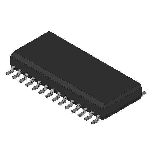
PG-DSO-28-22
Description
The BTM7751G is part of the TrilithIC family containing three dies in one package: One double high-side switch
and two low-side switches. The drains of these three vertical DMOS chips are mounted on separated lead frames.
The sources are connected to individual pins, so the BTM7751G can be used in H-bridge- as well as in any other
configuration. Both the double high-side and the two low-side switches of the BTM7751G are manufactured in
SMART SIPMOS® technology which combines low RDS ON vertical DMOS power stages with CMOS circuitry for
control, protection and diagnosis.
Type
Package
Marking
BTM7751G
PG-DSO-28-22
BTM7751G
Data Sheet
3
Rev. 1.0, 2008-06-27
�BTM7751G
2
Pin Configuration
2.1
Pin Assignment
DL1
1
28 DL1
IL1
2
27 SL1
DL1
3
26 SL1
N.C.
4
25 DL1
DHVS
5
24 DHVS
GND
6
23 SH1
IH1
7
LS-Leadframe
22 SH1
HS-Leadframe
ST
8
21 SH2
IH2
9
20 SH2
DHVS 10
19 DHVS
N.C. 11
18 DL2
LS-Leadframe
Figure 1
Data Sheet
DL2 12
17 SL2
IL2 13
16 SL2
DL2 14
15 DL2
Pin Assignment BTM7751G (Top View)
4
Rev. 1.0, 2008-06-27
�BTM7751G
Table 1
Pin Definitions and Functions
Pin No.
Symbol Function
1, 3, 25, 28
DL1
Drain of low-side switch1, lead frame 1 1)
2
IL1
Analog input of low-side switch1
4
N.C.
not connected
5, 10, 19, 24 DHVS
Drain of high-side switches and power supply voltage, lead frame 2 1)
6
GND
Ground
7
IH1
Digital input of high-side switch1
8
ST
Status of high-side switches; open Drain output
9
IH2
Digital input of high-side switch2
11
N.C.
not connected
12, 14, 15, 18 DL2
Drain of low-side switch2, lead frame 3 1)
13
IL2
Analog input of low-side switch2
16,17
SL2
Source of low-side switch2
20,21
SH2
Source of high-side switch2
22,23
SH1
Source of high-side switch1
26,27
SL1
Source of low-side switch1
1) To reduce the thermal resistance these pins are direct connected via metal bridges to the lead frame.
Pins written in bold type need power wiring.
Data Sheet
5
Rev. 1.0, 2008-06-27
�BTM7751G
2.2
Terms
VS=12V
IS
CS
470nF
CL
100µF
IFH1,2
DHVS
IST LK
IST
5,10,19,24
ST
8
Diagnosis
VST
IIH1
VSTL
IH1
7
IH2
9
VIH1
GND
6
VIH2
RO1
RO2
Gate
Driver
20,21
12,14,15,18
IGND
22,23
1,3,25,28
Protection
IL1
2
-VFH2
-VFH1
Biasing and Protection
ILKCL
IIL1
VDSH1
Gate
Driver
VSTZ
IIH1
VDSH2
SH2
ISH2
DL2
IDL2
IDL LK 2
VUVON
SH1
ISH1
VUVOFF
DL1
IDL1
IDL LK 1
Gate
Driver
Protection
VIL1
IIL2
IL2
13
Gate
Driver
VIL th 1
26,27
VIL2
VIL th 2
Figure 2
16,17
SL1
SL2
ISCP L 1
ISCP L 2
ISL1
ISL2
VDSL1
VDSL2
-VFL1
-VFL2
Terms BTM7751G
Table 2
HS-Source-Current
Named during Short Circuit
Named during Leakage-Cond.
ISH1,2
ISCP H
IDL LK
Data Sheet
6
Rev. 1.0, 2008-06-27
�BTM7751G
3
Block Diagram
DHVS
5,10,19,24
8
ST
Diagnosis
IH1
7
Biasing and Protection
Gate
Driver
RO1
IH2
9
RO2
Gate
Driver
20,21
SH2
12,14,15,18
6
DL2
GND
22,23
1,3,25,28
Protection
2
IL1
SH1
DL1
Gate
Driver
Protection
13
Gate
Driver
IL2
26,27
SL1
Figure 3
Data Sheet
16,17
SL2
Block Diagram BTM7751G
7
Rev. 1.0, 2008-06-27
�BTM7751G
4
Circuit Description
4.1
Input Circuit
The control inputs IH1,2 consist of TTL/CMOS compatible Schmitt-Triggers with hysteresis. Buffer amplifiers are
driven by these stages and convert the logic signal into the necessary form for driving the power output stages.
The inputs are protected by ESD clamp-diodes. The inputs IL1 and IL2 are connected to the internal gate-driving
units of the N-channel vertical power-MOS-FETs.
4.2
Output Stages
The output stages consist of an low RDSON Power-MOS H-bridge. In H-bridge configuration, the D-MOS body
diodes can be used for freewheeling when communicating inductive loads. If the high-side switches are used as
single switches, positive and negative voltage spikes which occur when driving inductive loads are limited by
integrated power clamp diodes.
4.3
Short Circuit Protection
The outputs are protected against
– output short circuit to ground
– output short circuit to the supply voltage, and
– overload (load short circuit).
An internal OP-Amp controls the Drain-Source-Voltage by comparing the DS-Voltage-Drop with an internal
reference voltage. Above this trip point the OP-Amp reduces the output current depending on the junction
temperature and the drop voltage.
4.4
Overtemperature Protection
The high-side and the low-side switches also incorporate an over temperature protection circuit with hysteresis
which switches off the output transistors. In the case of the high-side switches, the status output is set to low.
4.5
Undervoltage Lockout
When VS reaches the switch-on voltage VUVON the IC becomes active with a hysteresis. The High-Side output
transistors are switched off if the supply voltage VS drops below the switch off value VUVOFF.
4.6
Open Load Detection
The open load detection of the BTM7751G works in OFF condition and is based on a voltage measurement at the
source of the high side switch. In order to use the open load detection SH2 has to be connected to Vcc via a pull
up resistor. Because this pull up resistor would connect the bridge output to the µC supply it needs to be
disconnected whenever the high side switch is on. This can be done by a transistor as shown in the application
example (Figure 4 “Application Example BTM7751G” on Page 15). To check for open load:
•
•
•
Set IH1 = IH2 = LOW (both high side switches off)
Set IL2 = LOW, IL1 = HIGH (only low side switch 1 is on)
Connect Rol (open load pull up) to 5V via transistor
If the load is connected properly it will pull down the voltage at SH2 to a value close to 0V.
If the load is disconnected the resistor will pull the voltage at SH2 to value close to Vcc.
If the voltage at SH2 is higher than the open load detection voltage VOUT(OL) then ST will be pulled down.
Data Sheet
8
Rev. 1.0, 2008-06-27
�BTM7751G
4.7
Status Flag
The status flag output is an open drain output with zener-diode which requires a pull-up resistor, as shown in the
application circuit in Figure 4 “Application Example BTM7751G” on Page 15. Various errors as listed in the
table “Diagnosis” are reported by switching the open drain output ST to low.
Table 3
Truth table and Diagnosis (valid only for the High-Side-Switches)
Flag
IH1
IH2
Inputs
Normal operation;
identical with functional truth table
Open load at high-side switch 1
Open load at high-side switch 2
Overtemperature high-side switch1
Overtemperature high-side switch2
Overtemperature both high-side switches
Under voltage
SH1 SH2 ST Remarks
Outputs
0
0
1
1
0
1
0
1
L
L
H
H
L
H
L
H
1
1
1
1
stand-by mode
switch2 active
switch1 active
both switches
active
0
1
X
X
X
X
0
1
Z
H
X
X
X
X
Z
H
0
1
0
1
detected
0
1
X
X
L
L
X
X
1
0
detected
X
X
0
1
X
X
L
L
1
0
detected
0
X
1
0
1
X
L
L
L
L
L
L
1
0
0
detected
detected
X
X
L
L
1
not detected
detected
Inputs:
Outputs:
Status:
0 = Logic LOW
Z = Output in tristate condition
1 = No error
1 = Logic HIGH
L = Output in sink condition
0 = Error
X = don’t care
H = Output in source condition
X = Voltage level undefined
Data Sheet
9
Rev. 1.0, 2008-06-27
�BTM7751G
5
Electrical Characteristics
5.1
Absolute Maximum Ratings
Absolute Maximum Ratings1)
– 40 °C < Tj < 150 °C
Pos.
Parameter
Symbol
Limit Values
Unit Remarks
min.
max.
VS
VS(SCP)
– 0.3
42
V
–
28
V
IS
IIH
VIH
–7
3)
A
TA = 25°C; tP < 100 ms
–5
5
mA
Pin IH1 and IH2
– 10
16
V
Pin IH1 and IH2
VST
IST
– 0.3
5.4
V
–5
5
mA
Pin ST
–
V
30
V
–
20
V
IDL
VIL
–7
3)
A
VIL = 0 V; ID ≤ 1 mA
VIL = 5 V
VIL = 10 V
TA = 25°C; tP < 100 ms
– 0.3
10
V
–
Tj
Tstg
– 40
150
°C
–
– 55
150
°C
–
VESD
VESD
VESD
VESD
–
2
kV
–
1
kV
–
2
kV
–
8
kV
High-Side-Switches (Pins DHVS, IH1,2 and SH1,2)
5.1.1
Supply voltage
5.1.2
Supply voltage for full short circuit
protection
5.1.3
HS-drain current2)
5.1.4
HS-input current
5.1.5
HS-input voltage
–
Status Output ST
5.1.6
Status pull up voltage
5.1.7
Status Output current
5.1.8
Low-Side-Switches (Pins DL1,2, IL1,2 and SL1,2)
5.1.9
VDSL
42
Supply voltage for short circuit protection VDSL(SCP) –
5.1.10
Drain-Source-Clamp voltage
5.1.11
2)
5.1.12
LS-drain current
5.1.13
LS-input voltage
Temperatures
5.1.14
Junction temperature
5.1.15
Storage temperature
ESD Protection4)
5.1.16
Input LS-Switch
5.1.17
Input HS-Switch
5.1.18
Status HS-Switch
5.1.19
Output LS and HS-Switch
1)
2)
3)
4)
all other pins connected
to Ground
Not subject to production test; specified by design
Single pulse
Internally limited
ESD susceptibility HBM according to EIA/JESD22-A114-B (1.5kΩ, 100pF)
Note: Stresses above the ones listed here may cause permanent damage to the device. Exposure to absolute
maximum rating conditions for extended periods may affect device reliability.
Note: Integrated protection functions are designed to prevent IC destruction under fault conditions described in the
data sheet. Fault conditions are considered as “outside” normal operating range. Protection functions are
not designed for continuous repetitive operation.
Data Sheet
10
Rev. 1.0, 2008-06-27
�BTM7751G
5.2
Pos.
Functional Range
Parameter
Symbol Limit Values
min.
max.
Unit
Remarks
5.2.20
Supply voltage
VS
VUVOFF
42
V
After VS rising above
VUVON
5.2.21
Input voltage HS
– 0.3
15
V
–
5.2.22
Input voltage LS
– 0.3
10
V
–
5.2.23
Status output current
0
2
mA
–
5.2.24
Junction temperature
VIH
VIL
IST
Tj
– 40
150
°C
–
Note: Within the functional range the IC operates as described in the circuit description. The electrical
characteristics are specified within the conditions given in the related electrical characteristics table
5.3
Pos.
Thermal Resistance
Parameter
Symbol
5.3.25
LS-junction to soldering point1)
5.3.26
1)
5.3.27
HS-junction to soldering point
1)
Junction to Ambient
RthJA = Tj(HS) / (P(HS)+ P(LS))
RthJSP
RthJSP
RthJA
Limit Values
Unit
Conditions
20
K/W
measured to pin 3 or 12
20
K/W
measured to pin 19
K/W
2)
Min.
Typ.
Max.
–
–
–
–
–
36
–
1) Not subject to production test, specified by design.
2) Specified RthJA value is according to Jedec JESD51-2,-5,-7 at natural convection on FR4 2s2p board; The Product
(chip+package) was simulated on a 76.2 x 114.3 x 1.5 mm board with 2 inner copper layers (2 x 70µm Cu, 2 x 35µm Cu).
Data Sheet
11
Rev. 1.0, 2008-06-27
�BTM7751G
5.4
Electrical Characteristics
ISH1 = ISH2 = ISL1 = ISL2 = 0 A; – 40 °C < Tj < 150 °C; 8 V < VS < 18 V
unless otherwise specified
Pos.
Parameter
Symbol
Limit Values
Unit Test Condition
min.
typ.
max.
–
5
9
μA
IH1 = IH2 = 0 V
Tj = 25 °C
–
–
13
μA
IH1 = IH2 = 0 V
2.1
4.3
mA
Current Consumption HS-switch
5.4.28
Quiescent current
IS
Supply current;
one HS-switch active
IS
–
5.4.30
Supply current;
both HS-switches active
IS
–
4.3
8.6
mA
IH1 and IH2 = 5 V
VS = 12 V
5.4.31
Leakage current of
high-side switch
ISH LK
–
–
6
μA
5.4.32
Leakage current through logic GND
in free wheeling condition
ILKCL = IFH + –
ISH
–
10
mA
VIH = VSH = 0 V
VS = 12 V
IFH = 3 A
VS = 12 V
IIL
–
8
30
μA
VIL = 5 V;
normal operation
–
160
300
μA
VIL = 5 V;
IDL LK
–
2
10
μA
VIL = 0 V
VDSL = 18 V
VUVON
VUVOFF
VUVHY
–
–
4.8
V
1.8
–
3.5
V
–
1
–
V
VS increasing
VS decreasing
VUVON – VUVOFF
5.4.29
IH1 or IH2 = 5 V
VS = 12 V
Current Consumption LS-switch
5.4.33
Input current
failure mode
5.4.34
Leakage current of low-side switch
Under Voltage Lockout HS-switch
5.4.35
Switch-ON voltage
5.4.36
Switch-OFF voltage
5.4.37
Switch ON/OFF hysteresis
Output stages
5.4.38
Inverse diode of high-side switch;
Forward-voltage
VFH
–
0.8
1.2
V
IFH = 3 A
5.4.39
Inverse diode of low-side switch;
Forward-voltage
VFL
–
0.8
1.2
V
IFL = 3 A
5.4.40
Static drain-source on-resistance of
high-side switch
RDS ON H
–
70
–
mΩ
–
125
180
mΩ
–
45
–
mΩ
–
75
105
mΩ
ISH = 1 A; VS = 12 V
Tj = 25 °C
ISH = 1 A; VS = 12 V
Tj = 150 °C
ISL = 1 A; VIL = 5 V
Tj = 25 °C
ISL = 1 A; VIL = 5 V
Tj = 150 °C
5.4.41
Static drain-source
on-resistance of low-side switch
Data Sheet
RDS ON L
12
Rev. 1.0, 2008-06-27
�BTM7751G
ISH1 = ISH2 = ISL1 = ISL2 = 0 A; – 40 °C < Tj < 150 °C; 8 V < VS < 18 V
unless otherwise specified
Pos.
Parameter
Symbol
Limit Values
Unit Test Condition
min.
typ.
max.
15
19
23
A
Tj = – 40 °C
–
14
–
A
Tj = + 25 °C
8
10
13
A
Tj = + 150 °C
RO
8
15
35
kΩ
VDSL = 3 V
ISCP L
23
28
34
A
Tj = – 40 °C
–
22
–
A
Tj = 25 °C
11.5
14
18
A
Tj = 150 °C
Short Circuit of high-side switch to GND
5.4.42
Initial peak SC current
tdel = 100 µs; VS = 12 V; VDSH = 12V
ISCP H
Short Circuit of high-side switch to VS
5.4.43
Output pull-down-resistor
Short Circuit of low-side switch to VS
5.4.44
Initial peak SC current
VDSL = 12V; VIL = 5V;
tdel = 250 µs
1)
Thermal Shutdown
5.4.45
Thermal shutdown junction
temperature
Tj SD
155
180
190
°C
–
5.4.46
Thermal switch-on junction
temperature
Tj SO
150
170
180
°C
–
5.4.47
Temperature hysteresis
ΔΤ
–
10
–
°C
ΔΤ = TjSD – TjSO
VST L
IST LK
VST Z
–
0.2
0.6
V
IST = 1.6 mA
–
–
10
μA
VST = 5 V
5.4
–
–
V
IST = 1.6 mA
1.8
2.8
4
V
–
–
500
μs
Status Flag Output ST of high-side switch
5.4.48
Low output voltage
5.4.49
Leakage current
5.4.50
Zener-limit-voltage
Open load detection in Off condition
5.4.51
5.4.52
VOUT(OL)
Status change after neg. input slope td(OL)
Open load detection voltage
VS = 12 V
with OL
Data Sheet
13
Rev. 1.0, 2008-06-27
�BTM7751G
ISH1 = ISH2 = ISL1 = ISL2 = 0 A; – 40 °C < Tj < 150 °C; 8 V < VS < 18 V
unless otherwise specified
Pos.
Parameter
Symbol
Limit Values
Unit Test Condition
min.
typ.
max.
tON
tOFF
dV/dtON
-dV/dtOFF
–
85
180
μs
–
80
180
μs
–
–
1.2
V/μs
–
–
1.6
V/μs
–
60
150
μs
–
60
150
μs
1)
Switching times of high-side switch
5.4.53
Turn-ON-time to 90% VSH
5.4.54
Turn-OFF-time to 10% VSH
5.4.55
Slew rate on 10 to 30% VSH
5.4.56
Slew rate off 70 to 40% VSH
RLoad = 12 Ω
VS = 12 V
1)
Switching times of low-side switch
RLoad = 10 Ω
VS = 12 V
VIL = 0 to 5 V
5.4.57
Turn-ON-time to 10% VDL
5.4.58
Turn-OFF-time to 90% VDL
tON
tOFF
5.4.59
Slew rate on 70 to 50% VDL
-dV/dtON
–
1
1.5
5.4.60
Slew rate off 50 to 70% VDL
dV/dtOFF
–
1
1.5
V/μs RLoad = 4.7 Ω
V/μs VS = 12 V
VIL = 0 to 5 V
VIH High
VIH Low
VIH HY
IIH High
IIH Low
RI
VIH Z
–
–
2.5
V
–
1
–
–
V
–
–
0.3
–
V
–
15
30
60
μA
5
–
20
μA
VIH = 5 V
VIH = 0.4 V
2.7
4
5.5
kΩ
–
5.4
–
–
V
IIH = 1.6 mA
VIL th
0.9
1.7
2.2
V
IDL = 2 mA
Control Inputs of high-side switches IH 1, 2
5.4.61
H-input voltage
5.4.62
L-input voltage
5.4.63
Input voltage hysteresis
5.4.64
H-input current
5.4.65
L-input current
5.4.66
Input series resistance
5.4.67
Zener limit voltage
Control Inputs IL1, 2
5.4.68
Gate-threshold-voltage
1) Not subject to production test; specified by design
Note: The listed characteristics are ensured over the operating range of the integrated circuit. Typical
characteristics specified mean values expected over the production spread. If not otherwise specified,
typical characteristics apply at TA = 25 °C and the given supply voltage.
Data Sheet
14
Rev. 1.0, 2008-06-27
�BTM7751G
6
Application Information
Note: The following simplified application examples are given as a hint for the implementation of the device only
and shall not be regarded as a description or warranty of a certain functionality, condition or quality of the
device. The function of the described circuits must be verified in the real application
Watchdog
Reset
Q
RQ
100 kΩ
WD R
CQ
22µF
TLE
4278G
I
VS=12V
D
CS
10µF
D01
Z39
CD
47nF
VCC
DHVS
BCR192W
5,10,19,24
RS
ST
8
to µC
10 kΩ
Diagnosis
Biasing and Protection
ROL
10 kΩ
IH1
7
IH2
9
GND
6
optional for
open load
in off
Gate
Driver
RO1
XC866
µP
RO2
Gate
Driver
20,21
12,14,15,18
22,23
1,3,25,28
Protection
IL1
2
SH2
DL2
SH1
M
DL1
Gate
Driver
Protection
IL2
13
Gate
Driver
26,27
GND
SL1
16,17
SL2
In case of VDSL