Datasheet, Rev. 1.1, February 2008
BTS3160D
10mOhm Smart Low Side Power Switch
Automotive Power
�Smart Low Side Power Switch
HITFET - BTS3160D
Table of Contents
Table of Contents
Table of Contents . . . . . . . . . . . . . . . . . . . . . . . . . . . . . . . . . . . . . . . . . . . . . . . . . . . . . . . . . . . . . . . . 2
1
Overview . . . . . . . . . . . . . . . . . . . . . . . . . . . . . . . . . . . . . . . . . . . . . . . . . . . . . . . . . . . . . . . . . . . . . . . 3
2
2.1
Block Diagram . . . . . . . . . . . . . . . . . . . . . . . . . . . . . . . . . . . . . . . . . . . . . . . . . . . . . . . . . . . . . . . . . . . 5
Voltage and current naming definition . . . . . . . . . . . . . . . . . . . . . . . . . . . . . . . . . . . . . . . . . . . . . . . . . 6
3
3.1
3.2
Pin Configuration . . . . . . . . . . . . . . . . . . . . . . . . . . . . . . . . . . . . . . . . . . . . . . . . . . . . . . . . . . . . . . . . 7
Pin Assignment BTS3160D . . . . . . . . . . . . . . . . . . . . . . . . . . . . . . . . . . . . . . . . . . . . . . . . . . . . . . . . . 7
Pin Definitions and Functions . . . . . . . . . . . . . . . . . . . . . . . . . . . . . . . . . . . . . . . . . . . . . . . . . . . . . . . . 7
4
4.1
4.2
4.3
General Product Characteristics . . . . . . . . . . . . . . . . . . . . . . . . . . . . . . . . . . . . . . . . . . . . . . . . . . . .
Absolute Maximum Ratings . . . . . . . . . . . . . . . . . . . . . . . . . . . . . . . . . . . . . . . . . . . . . . . . . . . . . . . . .
Functional Range . . . . . . . . . . . . . . . . . . . . . . . . . . . . . . . . . . . . . . . . . . . . . . . . . . . . . . . . . . . . . . . . .
Thermal Resistance . . . . . . . . . . . . . . . . . . . . . . . . . . . . . . . . . . . . . . . . . . . . . . . . . . . . . . . . . . . . . . .
5
5.1
5.1.1
5.2
5.2.1
5.3
Supply and Input Stage . . . . . . . . . . . . . . . . . . . . . . . . . . . . . . . . . . . . . . . . . . . . . . . . . . . . . . . . . .
Supply Circuit . . . . . . . . . . . . . . . . . . . . . . . . . . . . . . . . . . . . . . . . . . . . . . . . . . . . . . . . . . . . . . . . . . .
Under Voltage Lock Out / Power On Reset . . . . . . . . . . . . . . . . . . . . . . . . . . . . . . . . . . . . . . . . . . .
Input Circuit . . . . . . . . . . . . . . . . . . . . . . . . . . . . . . . . . . . . . . . . . . . . . . . . . . . . . . . . . . . . . . . . . . . . .
Readout of Fault Information . . . . . . . . . . . . . . . . . . . . . . . . . . . . . . . . . . . . . . . . . . . . . . . . . . . . . .
Electrical Characteristics Supply and Input Stages . . . . . . . . . . . . . . . . . . . . . . . . . . . . . . . . . . . . . .
11
11
11
12
12
13
6
6.1
6.2
6.3
6.4
Power Stage . . . . . . . . . . . . . . . . . . . . . . . . . . . . . . . . . . . . . . . . . . . . . . . . . . . . . . . . . . . . . . . . . . .
Output On-state Resistance . . . . . . . . . . . . . . . . . . . . . . . . . . . . . . . . . . . . . . . . . . . . . . . . . . . . . . . .
Output Timing and Slopes . . . . . . . . . . . . . . . . . . . . . . . . . . . . . . . . . . . . . . . . . . . . . . . . . . . . . . . . .
Inductive Output Clamp . . . . . . . . . . . . . . . . . . . . . . . . . . . . . . . . . . . . . . . . . . . . . . . . . . . . . . . . . . .
Electrical Characteristics Power Stage . . . . . . . . . . . . . . . . . . . . . . . . . . . . . . . . . . . . . . . . . . . . . . . .
14
14
17
18
20
7
7.1
7.2
7.3
7.4
Protection Functions . . . . . . . . . . . . . . . . . . . . . . . . . . . . . . . . . . . . . . . . . . . . . . . . . . . . . . . . . . . .
Thermal Protection . . . . . . . . . . . . . . . . . . . . . . . . . . . . . . . . . . . . . . . . . . . . . . . . . . . . . . . . . . . . . . .
Over Voltage Protection . . . . . . . . . . . . . . . . . . . . . . . . . . . . . . . . . . . . . . . . . . . . . . . . . . . . . . . . . . .
Short Circuit Protection . . . . . . . . . . . . . . . . . . . . . . . . . . . . . . . . . . . . . . . . . . . . . . . . . . . . . . . . . . . .
Electrical Characteristics Protection . . . . . . . . . . . . . . . . . . . . . . . . . . . . . . . . . . . . . . . . . . . . . . . . . .
22
22
22
22
25
8
8.1
8.2
Application Information . . . . . . . . . . . . . . . . . . . . . . . . . . . . . . . . . . . . . . . . . . . . . . . . . . . . . . . . . . 26
Dimensioning of serial Resistor at IN pin . . . . . . . . . . . . . . . . . . . . . . . . . . . . . . . . . . . . . . . . . . . . . . 26
Further Application Information . . . . . . . . . . . . . . . . . . . . . . . . . . . . . . . . . . . . . . . . . . . . . . . . . . . . . . 27
9
Package Outlines . . . . . . . . . . . . . . . . . . . . . . . . . . . . . . . . . . . . . . . . . . . . . . . . . . . . . . . . . . . . . . . 28
10
Revision History . . . . . . . . . . . . . . . . . . . . . . . . . . . . . . . . . . . . . . . . . . . . . . . . . . . . . . . . . . . . . . . . 29
Datasheet
2
8
8
9
9
Rev. 1.1, 2008-02-28
�BTS3160D
Smart Low Side Power Switch
HITFET - BTS3160D
1
Overview
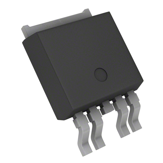
The BTS3160D is a one channel low-side power switch in
PG-TO-252-5-13 package providing embedded protective functions.
The power transistor is realized by a N-channel vertical power
MOSFET.
The device is controlled by a chip in Smart Power Technology.
PG-TO-252-5-13
Features
•
•
•
•
•
•
•
Logic level input compatible to 3.3 V or 5V micro controllers
Supply by Vbb line, down to 6 V
Very low over all leakage current
Providing digital fault information
Electrostatic discharge protection (ESD)
Green Product (RoHS compliant)
AEC Qualified
Table 1
Basic Electrical Data
Drain voltage
VD
40 V
Supply voltage
VS
6.0 … 45 V
On-State resistance at 25°C
RDS(ON,max) 10 mΩ
Nominal load current
IDnom
7.8 A
Maximum inrush current
IDSC
70 A
Leakage current MOSFET at Vbb = 13.5 V, TJ = 85 °C
IDSS
2 µA
Supply current in off mode at Vbb = 13.5 V, TJ = 85 °C
ISSS
4 µA
Clamping Energy
EAS
0.3 J
Type
Package
BTS3160D
PG-TO-252-5-13
Datasheet
3
Rev. 1.1, 2008-02-28
�Smart Low Side Power Switch
HITFET - BTS3160D
Overview
Digital Diagnostic
•
•
•
Over temperature shutdown
Over load shutdown
Short circuit shutdown
Protection Functions
•
•
•
•
Electrostatic discharge (ESD)
Under voltage lock out
Over temperature (shutdown with latch)
Over voltage (active clamped)
Application
•
•
•
•
•
Micro controller compatible low side power switch with digital feedback for 12V loads
All types of resistive, inductive and capacitive loads
Suitable for loads with high inrush current, such as lamps
Also suitable for LEDs because of low leakage current
Replaces electromechanical relays, fuses and discrete circuits
Description
The BTS3160D is a latching one channel low-side power switch in PG-TO-252-5-13 package providing embedded
protective functions. The power transistor is build by a N-channel vertical power MOSFET. The device is controlled
by a control chip in Smart Power Technology.
The device is able to switch all kind of resistive, inductive and capacitive loads. For lamp loads the lamp-inrushcurrent, eight- to ten-times the nominal current, has to be considered. The maximal inrush current has to be below
the minimum short circuit shutdown current.
The ESD protection of the VS and IN/Fault pin is in relation to GND.
The BTS3160D is supplied by the VS Pin. This Pin can be connected to battery line. The supply voltage is
monitored by the under voltage lock out circuit. The Gate driving unit allows to operate the device in the low ohmic
range even with 3.3 V input signal. For PWM application the device offers smooth turn-on and off due to the
embedded edge shaping function, in order to reduce EMC noise.
The over voltage protection is for protection during load-dump or inductive turn off conditions. The power MOSFET
is limiting the drain-source voltage, if it gets too high. This function is available even without supply.
The over temperature protection is in order to save the device from overheating due to overload and bad cooling
conditions. In order to reduce the device stress the edge shaping is disabled during thermal shutdown. After
thermal shutdown the device stays off until the latch is reset by a IN-Low signal. For high dynamic overload
conditions such as short circuit the device will turn off if a certain load current is reached. The short circuit
shutdown is a latch function. The device will stay off until the latch is reset by IN-Low signal. In order to reduce the
device stress the edge shaping is disabled during short circuit turn off.
Datasheet
4
Rev. 1.1, 2008-02-28
�Smart Low Side Power Switch
HITFET - BTS3160D
Block Diagram
2
Block Diagram
VS
IN /
Fault
Under
voltage
lockout
Gate
Driving
Unit
Drain
Overvoltage
Protection
Overtemperature
Protection
ϑ
Error
Logic
Short
circuit
Protection
ESD
Protection
GND
B loc k Diagram.emf
Figure 1
Datasheet
Block Diagram for the BTS3160D
5
Rev. 1.1, 2008-02-28
�Smart Low Side Power Switch
HITFET - BTS3160D
Block Diagram
2.1
Voltage and current naming definition
Following figure shows all the terms used in this datasheet, with associated convention for positive values.
Vbb
Vbb
IS
VS
RL
VS
Drain
I IN
VIN
IN / Fault
ID
VD
GND
I GND
GND
Terms .emf
Figure 2
Datasheet
Terms
6
Rev. 1.1, 2008-02-28
�Smart Low Side Power Switch
HITFET - BTS3160D
Pin Configuration
3
Pin Configuration
3.1
Pin Assignment BTS3160D
(top view)
Drain
6 (Tab)
5
GND
4
GND
3
2
IN / Fault
1
VS
P inConfiguration.emf
Figure 3
Pin Configuration PG-TO-252-5-13
3.2
Pin Definitions and Functions
Pin
Symbol
Function
1
VS
Supply Voltage; Connected to Battery Voltage with Reverse polarity protection
2
IN
Control Input and Status Feedback; Digital input 3.3 V or 5 V logic.
3, Tab Drain
Drain output; Protected low side power output channel
4,5
Ground; Signal ground, Pin 4 and 5 must be externally shorted1)
GND
1) Not shorting pin 4 and 5 will considerably increase the on-state resistance and reduce the peak current capability.
Datasheet
7
Rev. 1.1, 2008-02-28
�Smart Low Side Power Switch
HITFET - BTS3160D
General Product Characteristics
4
General Product Characteristics
4.1
Absolute Maximum Ratings
Absolute Maximum Ratings 1)
Tj = -40 °C to +150 °C; VS = 6 V to 30 V.
All voltages with respect to ground, positive current flowing into pin (unless otherwise specified)
Pos.
Parameter
Symbol
Limit Values
Min.
Max.
Unit
Conditions
Voltages
4.1.1
Supply voltage
VS
-0.3
30
V
–
4.1.2
Supply voltage during active clamping
VS(pulse)
-0.3
45
V
2)
4.1.3
Drain voltage
VD
-0.3
40
V
3)
4.1.4
Drain voltage for short circuit protection VD(SC)
0
30
V
–
4.1.5
Logic input voltage
VIN
-0.3
5.3
V
–
4.1.6
Unclamped single pulse inductive
energy
EAS
0
0.3
J
ID = 20 A;
Vbb = 30 V
TJ(Start) = 150°C
4.1.7
Load dump protection
VLoadDump = VA + VS
VLD
0
45
V
TJ = 25°C
Tj
Tstg
-40
150
°C
–
-55
150
°C
–
VESD
-4
4
kV
HBM4)
Energies
Temperatures
4.1.8
Junction Temperature
4.1.9
Storage Temperature
ESD Susceptibility
4.1.10
ESD Resistivity
on all pins
1)
2)
3)
4)
Not subject to production test, specified by design.
Not for DC operation, only for short pulse (i.e. loaddump) for a total of 100 h in full device life.
Active clamped.
ESD susceptibility, HBM according to EIA/JESD 22-A114B
Note: Stresses above the ones listed here may cause permanent damage to the device. Exposure to absolute
maximum rating conditions for extended periods may affect device reliability.
Note: Integrated protection functions are designed to prevent IC destruction under fault conditions described in the
data sheet. Fault conditions are considered as “outside” normal operating range. Protection functions are
not designed for continuous repetitive operation.
Datasheet
8
Rev. 1.1, 2008-02-28
�Smart Low Side Power Switch
HITFET - BTS3160D
General Product Characteristics
4.2
Pos.
Functional Range
Parameter
Symbol
Limit Values
Min.
Typ.
Max.
Unit
Conditions
4.2.1
Supply Voltage
VS
6
13.5
30
V
–
4.2.2
Supply current in off mode
IS(OFF)
–
1.5
–
µA
VIN = 0.0 V;
VS = 13.5 V;
TJ = 25 °C
–
–
4
VIN = 0.0 V;
VS = 13.5 V;
TJ = 85 °C1)
–
–
10
VIN = 0.0 V;
VS = 13.5 V;
TJ = 150 °C
–
1.6
3
4.2.3
Supply current in on
IS
mA
VIN = 5.0 V;
VS = 30 V
1) Not subject to production test, specified by design.
Note: Within the functional range the IC operates as described in the circuit description. The electrical
characteristics are specified within the conditions given in the related electrical characteristics table.
4.3
Pos.
Thermal Resistance
Parameter
4.3.1
Junction to Case
4.3.2
Junction to Ambient
Symbol
RthJC
RthJA
Limit Values
Min.
Typ.
Max.
–
0.9
1.1
–
80
–
45
Unit
Conditions
K/W
1)
K/W
1)
K/W
1)
@min. footprint
@ 6 cm² cooling
area, see Figure 4
1) Not subject to production test, specified by design
Datasheet
9
Rev. 1.1, 2008-02-28
�Smart Low Side Power Switch
HITFET - BTS3160D
General Product Characteristics
K/W
102
D = 0.5
101
D = 0.2
D = 0.1
ZthJA
D = 0.05
1
D = 0.02
D = 0.01
Single pulse
10-1
10-6
10-5
10-4
10-3
10-2
10-1
1
101
102
103 s
tp
Zth.emf
Figure 4
Typical transient thermal impedance
ZthJA = f(tp) , D = tp/T, Ta = 25 °C
Device on 50 mm × 50 mm × 1.5 mm epoxy PCB FR4 with 6 cm2 (one layer, 70 µm thick) copper area for
drain connection. PCB mounted vertical without blown air.
Datasheet
10
Rev. 1.1, 2008-02-28
�Smart Low Side Power Switch
HITFET - BTS3160D
Supply and Input Stage
5
Supply and Input Stage
5.1
Supply Circuit
The Supply pin VS is protected against ESD pulses as shown in Figure 5. Due to an internal voltage regulator the
device can be supplied from battery line.
6.0V ...30 V
VS
Regulator
ZD
GND
Figure 5
Supply Circuit
5.1.1
Under Voltage Lock Out / Power On Reset
S upply.emf
In order to ensure a stable device behavior under all allowed conditions the Supply voltage VS is monitored by the
under voltage lock out circuit. All device functions and protection are given for supply voltages above under voltage
lockout VSUVON but parameter deviations are possible below VS(min). There is no failure feedback for VS < VSUVON.
Device
functional
off
VSUVOFF
Figure 6
Datasheet
VS
VSUVON
UV LO_Hys teresis .emf
Under Voltage Lock Out
11
Rev. 1.1, 2008-02-28
�Smart Low Side Power Switch
HITFET - BTS3160D
Supply and Input Stage
5.2
Input Circuit
Figure 7 shows the input circuit of the BTS3160D. It’s ensured that the device switches off in case of open input
pin. A zener structure protects the input circuit against ESD pulses. As the BTS3160D has a supply pin, the
operation of the power MOS can be maintained regardless of the voltage on the IN pin, therefore a digital status
feedback down to logic low is realized. For readout of the fault information, please refer to “Readout of Fault
Information” on Page 12
IN/Fault
20µA
:
100µA
1.0mA
:
3.0mA
GND
input.emf
Figure 7
Input Circuit
5.2.1
Readout of Fault Information
The BTS3160D provides digital status information via an increased current on the IN / Fault pin.
The voltage on this pin is pulled down to logic low if a proper resistor is used. An example for the required circuitry
is shown in Figure 8.
The increased current IIN(fault) is an order of magnitude above the normal operation current IIN(nom) therefore the
voltage at the IN/Fault pin will decrease. The voltage at the pin is determined by the current and the serial resistor.
We recommend 3k3 for a 3.3V µC and 5k6 for a 5V µC to achieve a logic low signal.
For detailed calculation please refer to “Dimensioning of serial Resistor at IN pin” on Page 26
V bb
V CC
V CC
VS
Micro
controller
BTS3160D
DO
R1
I DO
I IN
IN/Fault
DI
GND
GND
VDI
GND
Figure 8
Datasheet
Fault_Readout.emf
Readout of Fault Information
12
Rev. 1.1, 2008-02-28
�Smart Low Side Power Switch
HITFET - BTS3160D
Supply and Input Stage
5.3
Electrical Characteristics Supply and Input Stages
VS = 6 V to 30 V, Tj = -40 °C to +150 °C
All voltages with respect to ground, positive current flowing into pin (unless otherwise specified)
Pos.
Parameter
Symbol
Limit Values
Min.
Typ.
Max.
Unit
Conditions
Under Voltage Lockout
5.3.1
UV-switch-on voltage
VSUVON
–
–
5.5
V
VS = 5.5 V
5.3.2
UV-switch-off voltage
VSUVOFF
4.0
–
–
V
VS = 4.0 V
5.3.3
UV-switch-off hysteresis
VSUVHY
–
0.2
–
V
VSUVON - VSUVOFF
Digital Input / Fault Feedback
5.3.4
Low level voltage
VINL
–
–
0.8
V
VS = 6 V;
no fault condition
5.3.5
High level voltage
VINH
2.0
–
–
V
VS = 6 V;
no fault condition
5.3.6
Input pull down current
IIN
20
50
100
µA
VIN = 5.3 V;
no fault condition
IIN-Fault
1
2
3
mA
VIN = 5.3 V;
all fault conditions
600
uA
1)
5.3.7
Input Fault ON threshold
IFault_ONth
1) not subject to production test
Datasheet
13
Rev. 1.1, 2008-02-28
�Smart Low Side Power Switch
HITFET - BTS3160D
Power Stage
6
Power Stage
The power stage is built by a N-channel vertical power MOSFET (DMOS)
6.1
Output On-state Resistance
The on-state resistance depends on the supply voltage as well as on the junction temperature TJ. Figure 9 shows
the dependency over temperature for the typical on-state resistance RDS(on),while Figure 10 shows the
dependency over Vs.
VS=10V
RDS(on) [ mΩ ]
16,00
14,00
12,00
typ.
10,00
8,00
6,00
4,00
-40
-15
10
35
60
85
110 135 150
T [ °C ]
rds on_Tj.emf
Figure 9
Datasheet
Typical On-State Resistance
14
Rev. 1.1, 2008-02-28
�Smart Low Side Power Switch
HITFET - BTS3160D
Power Stage
50,00
45,00
R DS(on) [mΩ ]
40,00
35,00
30,00
25,00
20,00
typ.
15,00
10,00
5,00
0
10
20
30
VS [V]
rdson_V s.emf
Figure 10
Typical On-State Resistance RDSon = f(VS)
70
VS= 10V
60
& VS= 30V
VS = 6V
ID [A]
50
40
typ.
30
20
10
0
0
0,5
1
VDS [V]
Figure 11
Datasheet
1,5
Outputchar.emf
Typical Output Characteristics, TJstart = 25 °C, Parameter VS
15
Rev. 1.1, 2008-02-28
�Smart Low Side Power Switch
HITFET - BTS3160D
Power Stage
6,00
I DSS
[µA]
Idss
[µA]
4,00
2,00
typ.
0,00
-50 -25
0
25
50
75
100 125 150 175
Tj [°C]
TJ [°C]
Figure 12
Datasheet
Zeroindrain.emf
Typical Zero Input Voltage Drain Current, IDSS = f(TJ)
16
Rev. 1.1, 2008-02-28
�Smart Low Side Power Switch
HITFET - BTS3160D
Power Stage
6.2
Output Timing and Slopes
A high signal on the input pin causes the power MOSFET to switch on with a dedicated slope which is optimized
for low EMC emission. Figure 13 shows the timing definition.
IN
High
Low
VD
t on
t off
tond
t
toffd
V bb
90 %
60 %
-dVD / dto n
40 %
dV D / dtoff
10 %
t
OutputTiming.emf
Figure 13
Switching a resistive Load
In order to minimize the emission during switching the BTS3160D limits the slopes during turn on- and off to slow
slew rate settings.The definition is shown in Figure 14. For best performance of the edge shaping the supply pin VS
should be connected to battery voltage. For supply voltages other than nominal battery the edge shaping can differ
from the values in the electrical characteristics table below.
IN
High
Low
t
ID
100 %
|di/dt|slow
80 %
|di/dt|fast
20 %
|di/dt|slow
t
E dgeS haping.emf
Figure 14
Datasheet
Typical Slopes for resistive Loads
17
Rev. 1.1, 2008-02-28
�Smart Low Side Power Switch
HITFET - BTS3160D
Power Stage
6.3
Inductive Output Clamp
When switching off inductive loads with low-side switches, the Drain Source voltage VD rises above battery
potential, because the inductance intends to continue driving the current.
The BTS3160D is equipped with a voltage clamp mechanism that keeps the Drain-Source voltage VD at a certain
level. See Figure 15 for more details.
Drain
GND
OutputClamp.emf
Figure 15
Output Clamp
Overtemperature or
short circuit detected
IN
High
Low
t
ID
t
Von
V DAZ
V bb
t
Induc tiv eLoad.emf
Figure 16
Switching an inductance
While demagnetization of inductive loads, energy has to be dissipated in the BTS3160D. This energy can be
calculated with following equation:
V bb – V DS(CL)
RL ⋅ IL
L
- ⋅ ln 1 – ---------------------------------E = V DS(CL) ⋅ ---------------------------------- + I L ⋅ -----RL
RL
V bb – V DS(CL)
Following equation simplifies under assumption of RL = 0
V bb
2
1
E = --- LI L ⋅ 1 – ----------------------------------
2
V
–
V
bb
DS(CL)
Datasheet
18
Rev. 1.1, 2008-02-28
�Smart Low Side Power Switch
HITFET - BTS3160D
Power Stage
Figure 17 shows the inductance / current combination the BTS3160D can handle.
For maximum single avalanche energy please also refer to EAS value in “Energies” on Page 8
L [mH]
10,0
Vbb = 30V
1,0
Max.
0,1
0,0
10
I D [A]
100
EAS.emf
Figure 17
Datasheet
Maximum load inductance for single pulse
L=f (IL), Tj,start= 150 °C
19
Rev. 1.1, 2008-02-28
�Smart Low Side Power Switch
HITFET - BTS3160D
Power Stage
6.4
Electrical Characteristics Power Stage
VS = 6 V to 30 V, Tj = -40 °C to +150 °C
All voltages with respect to ground, positive current flowing into pin (unless otherwise specified)
Pos.
Parameter
Symbol
Limit Values
Unit
Conditions
Min.
Typ.
Max.
–
8
10
mΩ
ID = 20 A;
VIN = high;
VS = 10 V;
TJ = 25 °C
–
14
18
mΩ
ID = 20 A;
VIN = high;
VS = 10 V;
TJ = 150 °C
Power Supply
6.4.1
On-state resistance
RDS(on)
6.4.2
Nominal load current
IDnom
7.8
9.7
–
A
1)
6.4.3
ISO load current
IDISO
33
41
–
A
1)
6.4.4
Off state drain current
IDSS
–
6
12
µA
Vbb = 32 V;
VIN = 0.0 V
–
1
2
µA
1)
6.4.5
Von = 0.5 V;
TA = 85 °C SMD2);
VIN = 5.0 V;
VS ≥ 10 V;
TJ < 150 °C
Von = 0.5 V;
TC = 85 °C;
VIN = 5.0 V;
VS ≥ 10 V;
TJ < 150 °C
Vbb = 13.5 V;
VIN = 0.0 V;
TJ = 85 °C
Dynamic Characteristics
6.4.6
Turn-on delay
tond
20
75
110
µs
RL = 2.2 Ω;
Vbb = VS = 13.5 V
6.4.7
Turn-on time
ton
80
150
250
µs
RL = 2.2 Ω;
Vbb = VS = 13.5 V
6.4.8
Turn-off delay
toffd
20
75
110
µs
RL = 2.2 Ω;
Vbb = VS = 13.5 V
6.4.9
Turn-off time
toff
80
150
250
µs
RL = 2.2 Ω;
Vbb = VS = 13.5 V
6.4.10
Slew rate on
-dVD/dton 0.1
0.3
0.7
V/µs
RL = 2.2 Ω;
Vbb = VS = 13.5 V
6.4.11
Slew rate off
dVD/dtoff
0.3
0.7
V/µs
RL = 2.2 Ω;
Vbb = VS = 13.5 V
6.4.12
Slew rate during edge shaping
|dI/dt|slow –
0.04
0.07
A/µs
1)
Datasheet
0.1
20
RL = 2.2 Ω
Vbb = VS = 13.5 V;
ohmic load
Rev. 1.1, 2008-02-28
�Smart Low Side Power Switch
HITFET - BTS3160D
Power Stage
VS = 6 V to 30 V, Tj = -40 °C to +150 °C
All voltages with respect to ground, positive current flowing into pin (unless otherwise specified)
Pos.
Parameter
Symbol
Limit Values
Min.
Typ.
Max.
Unit
Conditions
6.4.13
Slew rate between edge shaping
|dI/dt|fast
–
–
0.3
A/µs
1)
6.4.14
Fault signal delay
tdfault
–
4
10
µs
1)
VD
-0.3
-1.0
-1.5
V
ID = -12 A;
VS = 0 V;
VIN = 0.0 V
RL = 2.2 Ω
Vbb = VS = 13.5 V;
ohmic load
Inverse Diode
6.4.15
Inverse Diode forward voltage
1) Not subject to production test.
2) Device on 50 mm × 50 mm × 1.5 mm epoxy PCB FR4 with 6 cm2 (one layer, 70 µm thick) copper area for drain connection.
PCB mounted vertical without blown air.
Datasheet
21
Rev. 1.1, 2008-02-28
�Smart Low Side Power Switch
HITFET - BTS3160D
Protection Functions
7
Protection Functions
The device provides embedded protection functions against over temperature, over load and short circuit.
Note: Integrated protection functions are designed to prevent IC destruction under fault conditions described in the
data sheet. Fault conditions are considered as “outside” normal operation.
7.1
Thermal Protection
The device is protected against over temperature resulting due to overload and / or bad cooling conditions.
The BTS3160D has a thermal latch function. The thermal latch is reset by IN-Low signal. See Figure 18 for the
latch behavior.
The diagram naming refers to Figure 8
Thermal shutdown
IN
High
Low
t
TJ
TJSD
∆TJSD
tdfau lt
IIN
t
I INfault
I INno m
0
t
DI
High
Low
t
Thermal_fault_latch.emf
Figure 18
Status Feedback via Input Current at Over temperature
7.2
Over Voltage Protection
The BTS3160D is equipped with a voltage clamp mechanism that keeps the Drain-Source voltage VD at a certain
level. This stage is also used for inductive clamping.
See “Inductive Output Clamp” on Page 18 for details.
7.3
Short Circuit Protection
The condition short circuit is an overload condition of the device. Dependent on the short circuit resistance the
current increase is more or less steep. In condition of high ohmic short the device heats up and the turn off is due
to over temperature. In condition low ohmic short the device turns off on a threshold current level before the over
temperature condition is detected. In order to allow short current spikes, the turn off occurs with the delay time
tdSC. Figure 19 shows the behavior mentioned above. In this example the short circuit always occurs after the
device has switched on under normal load condition - Short circuit type 2. The definitions of voltages and currents
are in respect to Figure 8. The behavior of VDI also depends on RIN.
Datasheet
22
Rev. 1.1, 2008-02-28
�Smart Low Side Power Switch
HITFET - BTS3160D
Protection Functions
VDO
Overload
Thermal
shutdown
Short
circuit
Short Circuit
shut off
short spike
High
Low
ID
t
I DSC
t d sc
t d sc
I Dno m
tdfau lt
I IN
t dfau lt
t
I INfault
I INno m
0
t
V DI
High
Low
t
S hort circuit Ty pe 2.emf
Figure 19
IN
High
Short Circuit during On State, Typical Behavior for Ohmic Loads
Short Circuit
shut off
Thermal shutdown
short spike
Low
ID
t
I DSC
td sc
td sc
I Dn o m
I IN
t d fau lt
td fau lt
t
I INfau lt
I INn o m
0
t
DI
High
Low
t
S hort c irc uit Ty pe 1.emf
Figure 20
Turn On into Existing Short Circuit, Typical Behavior for Ohmic Loads
The case when the device switches on into an existing short circuit - Short circuit type 1- is shown in Figure 20.
Datasheet
23
Rev. 1.1, 2008-02-28
�Smart Low Side Power Switch
HITFET - BTS3160D
Protection Functions
The test setup for short circuit characterization is shown in Figure 21. The BTS3160D is a low side switch.
Therefore it can be assumed that the micro controller and device GND connection have a low impedance. The Vs
voltage needs to be stabilized to ensure the protection features. In application this is often already covered from
the module standard circuits.
RSC
ID
LSC
Vcc
VS
Drain
IN
V bb
5V
Control circuit
RIN
BTS3160
GND
GND
Figure 21
Datasheet
S etup_S hort_c irc uit.emf
Test Setup for Short Circuit Characterization Test
24
Rev. 1.1, 2008-02-28
�Smart Low Side Power Switch
HITFET - BTS3160D
Protection Functions
7.4
Electrical Characteristics Protection
VS = 6 V to 30 V, Tj = -40 °C to +150 °C
All voltages with respect to ground, positive current flowing into pin (unless otherwise specified)
Pos.
Parameter
Symbol
Limit Values
Min.
Typ.
Max.
Unit
Conditions
Thermal Protection
7.4.1
Thermal shut down junction
temperature
TJSD
150
1751)
–
°C
VS = 6.0 V
7.4.2
Thermal hysteresis
∆TJSD
–
10
–
K
1)
VDAZ
40
44
–
V
ID = 10 mA;
VS = 0.0 V;
VIN = 0.0 V
–
45
49
V
ID = 8 A;
VS = 0.0 V;
VIN = 0.0 V
VS = 6.0 V
Over Voltage Protection
7.4.3
Drain source clamp voltage
Short Circuit Protection, 6.0 V ≤ VS ≤ 30 V
7.4.4
Short circuit shutdown current for
max. tdSC
IDSC
70
100
130
A
7.4.5
Short circuit shutdown delay
tdSC
1
4
8
µs
1)
ID > ID(SC),
ohmic load
1) Not subject to production test, specified by design.
Datasheet
25
Rev. 1.1, 2008-02-28
�Smart Low Side Power Switch
HITFET - BTS3160D
Application Information
8
Application Information
Note: The following information is given as a hint for the implementation of the device only and shall not be
regarded as a description or warranty of a certain functionality, condition or quality of the device.
8.1
Dimensioning of serial Resistor at IN pin
In order to use the digital feedback function of the device, there is serial resistor necessary between the IN pin and
the driver (micro controller)
To calculate the value of this serial resistor on the input pin three device conditions as well as the driver (micro
controller) abilities needs to be taken into account.
The driver must be capable of driving at least IFault_ONth to avoid immediate restart
Figure 22 shows the circuit used for reading out the digital status.
V bb
Microcontroller
V CC
V CC
I DO
DO
VRIN
RIN
VS
IIN
BTS3160D
IN/Fault
DI
V DO
20µA
:
100µA
V DI
GND
GND
GND
Figure 22
Fault information
1.0mA
:
3.0mA
Fault_RIN.emf
Circuitry to readout fault information
Note: This is a very simplified example of an application circuit. The function must be verified in the real application.
Conditions to be meet by the circuitry:
•
•
•
During normal operation VIN must be higher than VINH,min to switch ON.
During fault condition the max. capability of the driver (micro controller) must not be exceeded and the logic
low level at DI must be ensured by a voltage drop over the serial resistor RIN while the device fault current is
flowing.
During fault state the device keeps protection active as long as it can sink more than the threshold current
IFault_ONth. In case the device can not sink this current, it resets the protection and waits for the next input high
signal. So to avoid an unintentional switch ON/OFF behavior, the input current must be above this threshold.
Datasheet
26
Rev. 1.1, 2008-02-28
�Smart Low Side Power Switch
HITFET - BTS3160D
Application Information
Conditions in formulas:
1. µCoutput current,min > µCHIGH,max / RIN > IFault_ONth
with µCoutput current,min referring to the micro controller maximum output current capability.
with µCHIGH,max referring to the maximal high output voltage of the micro controller driving stage.
This condition is valid during status feedback operation mode.
2. VIN = µCHIGH,min - (RIN * IIN,max) > VINH,min
with µCHIGH,min referring to the minimal high output voltage of the micro controller driving stage.
This condition is valid during normal operation mode
3. µCHIGH,max - (RIN * IIN-Fault,min) < µC(DI)L,max
with µC(DI)L,max referring to the maximum logic low voltage of the micro controller input stage
The maximum current is either defined by the BTS3160D or the micro controller driving stage
This condition is valid during status feedback operation mode
4. IIN-Fault= µCHIGH,min / RIN > IFault_ONth
with µCHIGH,min referring to the minimum logic low voltage of the micro controller output stage
The BTS3160D is resetting the fault latch, if the current on IN pin goes below IFault_ONth.
This condition is valid during status feedback operation mode
Out of this conditions the minimum and maximum resistor values can be calculated.
For a typical 5V micro controller with output current capability in the 3 mA range,
a resistor range from 7.5 kΩ down to 4.5 kΩ can be used.
For a typical 3.3V micro controller a range from 4.6 kΩ to 2.5 kΩ is suitable.
We recommend 3k3 for a 3.3V µC and 5k6 for a 5V µC to achieve a logic low signal.
8.2
•
Further Application Information
For further information you may contact http://www.infineon.com/hitfet
Datasheet
27
Rev. 1.1, 2008-02-28
�Smart Low Side Power Switch
HITFET - BTS3160D
Package Outlines
Package Outlines
A
5.7 MAX. 1)
B
9.98 ±0.5
6.22 -0.2
0.15 MAX.
per side
0.5 +0.08
-0.04
0.9 +0.20
-0.01
0...0.15
5 x 0.6 ±0.1
1.14
4.56
0.5 +0.08
-0.04
0.1 B
0.25
M
A B
1) Includes mold flashes on each side.
All metal surfaces tin plated, except area of cut.
Figure 23
2.3 +0.05
-0.10
(5)
0.8 ±0.15
1±0.1
(4.24)
6.5 +0.15
-0.05
0.51 MIN.
9
PG-TO252-5-13-PO V0.1
PG-TO-252-5-13 (Plastic Green Thin Outline Package)
Green Product (RoHS compliant)
To meet the world-wide customer requirements for environmentally friendly products and to be compliant with
government regulations the device is available as a green product. Green products are RoHS-Compliant (i.e
Pb-free finish on leads and suitable for Pb-free soldering according to IPC/JEDEC J-STD-020).
You can find all of our packages, sorts of packing and others in our
Infineon Internet Page “Products”: http://www.infineon.com/products.
Datasheet
28
Dimensions in mm
Rev. 1.1, 2008-02-28
�Smart Low Side Power Switch
HITFET - BTS3160D
Revision History
10
Version
Revision History
Date
Changes
Rev. 1.1
2008-02-28
released automotive green and robust version
changed package naming to green package, updated package drawing
updated package drawing and description text on overview page
added RoHS logo to overview page and added green feature to list
Rev. 1.0
2007-08-14
first released datasheet revision
Datasheet
29
Rev. 1.1, 2008-02-28
�Edition 2008-02-28
Published by
Infineon Technologies AG
81726 Munich, Germany
© 2008 Infineon Technologies AG
All Rights Reserved.
Legal Disclaimer
The information given in this document shall in no event be regarded as a guarantee of conditions or
characteristics. With respect to any examples or hints given herein, any typical values stated herein and/or any
information regarding the application of the device, Infineon Technologies hereby disclaims any and all warranties
and liabilities of any kind, including without limitation, warranties of non-infringement of intellectual property rights
of any third party.
Information
For further information on technology, delivery terms and conditions and prices, please contact the nearest
Infineon Technologies Office (www.infineon.com).
Warnings
Due to technical requirements, components may contain dangerous substances. For information on the types in
question, please contact the nearest Infineon Technologies Office.
Infineon Technologies components may be used in life-support devices or systems only with the express written
approval of Infineon Technologies, if a failure of such components can reasonably be expected to cause the failure
of that life-support device or system or to affect the safety or effectiveness of that device or system. Life support
devices or systems are intended to be implanted in the human body or to support and/or maintain and sustain
and/or protect human life. If they fail, it is reasonable to assume that the health of the user or other persons may
be endangered.
�