Smart High-Side Power Switch
BTS716G
6PDUW�+LJK�6LGH�3RZHU�6ZLWFK�
)RXU�&KDQQHOV����[����P�
6WDWXV�)HHGEDFN�
Product Summary
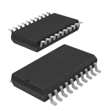
Package
9EE�
$FWLYH�FKDQQHOV�
2Q�VWDWH�5HVLVWDQFH�
521�
1RPLQDO�ORDG�FXUUHQW�
,/�120��
&XUUHQW�OLPLWDWLRQ�
,/�6&U��
2SHUDWLQJ�9ROWDJH�
RQH�
���P�
���$�
���$�
���������9�
IRXU�SDUDOOHO�
��P�
���$�
���$�
P-DSO-20
PG-DSO20
*HQHUDO�'HVFULSWLRQ�
•�
•�
1�FKDQQHO�YHUWLFDO�SRZHU�026)(7�ZLWK�FKDUJH�SXPS��JURXQG�UHIHUHQFHG�&026�FRPSDWLEOH�LQSXW�DQG�
GLDJQRVWLF�IHHGEDFN��PRQROLWKLFDOO\�LQWHJUDWHG�LQ�6PDUW�6,3026 �WHFKQRORJ\��
3URYLGLQJ�HPEHGGHG�SURWHFWLYH�IXQFWLRQV�
$SSOLFDWLRQV�
•�
•�
•�
•�
&�FRPSDWLEOH�KLJK�VLGH�SRZHU�VZLWFK�ZLWK�GLDJQRVWLF�IHHGEDFN�IRU���9�DQG���9�JURXQGHG�ORDGV�
$OO�W\SHV�RI�UHVLVWLYH��LQGXFWLYH�DQG�FDSDFLWYH�ORDGV�
0RVW�VXLWDEOH�IRU�ORDGV�ZLWK�KLJK�LQUXVK�FXUUHQWV��VR�DV�ODPSV�
5HSODFHV�HOHFWURPHFKDQLFDO�UHOD\V��IXVHV�DQG�GLVFUHWH�FLUFXLWV�
%DVLF�)XQFWLRQV�
•�
•�
•�
•�
•�
•�
•�
9HU\�ORZ�VWDQGE\�FXUUHQW�
&026�FRPSDWLEOH�LQSXW�
,PSURYHG�HOHFWURPDJQHWLF�FRPSDWLELOLW\��(0&��
)DVW�GHPDJQHWL]DWLRQ�RI�LQGXFWLYH�ORDGV�
6WDEOH�EHKDYLRXU�DW�XQGHUYROWDJH�
:LGH�RSHUDWLQJ�YROWDJH�UDQJH�
/RJLF�JURXQG�LQGHSHQGHQW�IURP�ORDG�JURXQG�
3URWHFWLRQ�)XQFWLRQV�
•�
•�
•�
•�
•�
•�
•�
•�
�
�
�
�
6KRUW�FLUFXLW�SURWHFWLRQ�
2YHUORDG�SURWHFWLRQ��
&XUUHQW�OLPLWDWLRQ�
7KHUPDO�VKXWGRZQ�
2YHUYROWDJH�SURWHFWLRQ��LQFOXGLQJ�ORDG�GXPS��ZLWK�H[WHUQDO�
UHVLVWRU�
5HYHUVH�EDWWHU\�SURWHFWLRQ�ZLWK�H[WHUQDO�UHVLVWRU�
/RVV�RI�JURXQG�DQG�ORVV�RI�9EE�SURWHFWLRQ�
(OHFWURVWDWLF�GLVFKDUJH�SURWHFWLRQ��(6'��
'LDJQRVWLF�)XQFWLRQ�
•�
•�
•�
9EE
,1�
67���
,1�
/RJLF
&KDQQHO��
&KDQQHO��
,1�
67���
/RJLF
&KDQQHO��
&KDQQHO��
*1'
1
/RDG��
/RDG��
,1�
'LDJQRVWLF�IHHGEDFN�ZLWK�RSHQ�GUDLQ�RXWSXW�
2SHQ�ORDG�GHWHFWLRQ�LQ�2))�VWDWH�
)HHGEDFN�RI�WKHUPDO�VKXWGRZQ�LQ�21�VWDWH�
Data Sheet
Block Diagram�
/RDG��
/RDG��
V1.0, 2007-05-13
�Smart High-Side Power Switch
BTS716G
)XQFWLRQDO�GLDJUDP��
�
�
�
�
�
�
�
�
�
�
�
�
�
�
�
�
RYHUYROWDJH�
SURWHFWLRQ
�
�
�
�
ORJLF�
LQWHUQDO�
YROWDJH�VXSSO\�
,1��
9%%
FODPS�IRU�
LQGXFWLYH�ORDG
�
�
(6'�
WHPSHUDWXUH�
VHQVRU�
UHYHUVH�
EDWWHU\�
SURWHFWLRQ�
2SHQ�ORDG��
GHWHFWLRQ�
�
�
�
�
FXUUHQW�OLPLW
287��
�
�
JDWH�
FRQWURO�
��
FKDUJH�
SXPS�
����
�
�
�
/2$'�
����������FKDQQHO���
67����
�
�
� ,1��
�
�
�
� *1'����
�
control and protection circuit
of
channel 2
287��
�
�
�
�
�
�
�
�
�
�
�
�
�
�
�
�
,1��
control and protection circuit
of
channel 3
287��
67����
IN4
�
�
� *1'����
�
�
�
�
�
�
�
control and protection circuit
of
channel 4
287��
�
Data Sheet
2
V1.0, 2007-05-13
�Smart High-Side Power Switch
BTS716G
Pin Definitions and Functions
Pin
1,10,
11,12,
15,16,
19,20
3
5
7
9
18
17
14
13
4
8
2
6
Data Sheet
Pin configuration
Symbol Function
Vbb
Positive power supply voltage. Design the
wiring for the simultaneous max. short circuit
currents from channel 1 to 2 and also for low
thermal resistance
IN1
Input 1,2,3,4 activates channel 1,2,3,4 in case
of logic high signal
IN2
IN3
IN4
OUT1
Output 1,2,3,4 protected high-side power output
of channel 1,2,3,4. Design the wiring for the
OUT2
max. short circuit current
OUT3
OUT4
ST1/2
Diagnostic feedback 1/2,3/4 of channel 1,2,3,4
ST3/4
open drain, low on failure
GND1/2 Ground of chip 1 (channel 1,2)
GND3/4 Ground of chip 2 (channel 3,4)
3
(top view)
Vbb
GND1/2
IN1
ST1/2
IN2
GND3/4
IN3
ST3/4
IN4
Vbb
1
2
3
4
5
6
7
8
9
10
•
20
19
18
17
16
15
14
13
12
11
Vbb
Vbb
OUT1
OUT2
Vbb
Vbb
OUT3
OUT4
Vbb
Vbb
V1.0, 2007-05-13
�Smart High-Side Power Switch
BTS716G
Parameter
Symbol
Supply voltage (overvoltage protection see page 6)
Supply voltage for full short circuit protection
Tj,start = -40 ...+150°C
Load current (Short-circuit current, see page 6)
Load dump protection1) VLoadDump = VA + Vs, VA = 13.5 V
RI2) = 2 Ω, td = 400 ms; IN = low or high,
each channel loaded with RL = 13.5 Ω,
Operating temperature range
Storage temperature range
Power dissipation (DC)4)
Ta = 25°C:
(all channels active)
Ta = 85°C:
Maximal switchable inductance, single pulse
Vbb = 12V, Tj,start = 150°C4), see diagrams on page 10
IL = 2.3 A, EAS = 76 mJ, 0 Ω
one channel:
IL = 3.3 A, EAS = 182 mJ, 0 Ω
two parallel channels:
IL = 4.7 A, EAS = 460 mJ, 0 Ω
four parallel channels:
Electrostatic discharge capability (ESD)
IN:
(Human Body Model)
ST:
out to all other pins shorted:
Vbb
Vbb
Values
Unit
43
36
V
V
IL
VLoad dump3)
self-limited
60
A
V
Tj
Tstg
Ptot
-40 ...+150
-55 ...+150
3.6
1.9
°C
ZL
21
25
30
mH
VESD
1.0
4.0
8.0
kV
-10 ... +16
±0.3
±5.0
±5.0
V
mA
W
acc. MIL-STD883D, method 3015.7 and ESD assn. std. S5.1-1993
R=1.5kΩ; C=100pF
Input voltage (DC) see internal circuit diagram page 9
Current through input pin (DC)
Pulsed current through input pin5)
Current through status pin (DC)
1)
2)
3)
4)
5)
VIN
IIN
IIN
IST
Supply voltages higher than Vbb(AZ) require an external current limit for the GND and status pins (a 150Ω
resistor for the GND connection is recommended.
RI = internal resistance of the load dump test pulse generator
VLoad dump is setup without the DUT connected to the generator per ISO 7637-1 and DIN 40839
Device on 50mm*50mm*1.5mm epoxy PCB FR4 with 6cm2 (one layer, 70µm thick) copper area for Vbb
connection. PCB is vertical without blown air. See page 14
only for testing
Data Sheet
4
V1.0, 2007-05-13
�Smart High-Side Power Switch
BTS716G
Parameter and Conditions
Thermal resistance
junction - soldering point6)7)
junction – ambient6)
@ 6 cm2 cooling area
Symbol
each channel: Rthjs
Rthja
one channel active:
all channels active:
Values
min
typ
max
Unit
17
----
K/W
Values
min
typ
max
Unit
-----
--44
35
Electrical Characteristics
Parameter and Conditions, each of the four channels
Symbol
at Tj = -40...+150°C, Vbb = 12 V unless otherwise specified
Load Switching Capabilities and Characteristics
On-state resistance (Vbb to OUT); IL = 2 A
each channel,
Tj = 25°C: RON
Tj = 150°C:
two parallel channels, Tj = 25°C:
four parallel channels, Tj = 25°C:
-----
110
210
55
28
140
280
70
35
mΩ
2.3
3.3
4.7
2.6
3.7
5.3
----
A
--
--
2
mA
---
100
100
250
270
µs
0.2
0.2
---
1.0
1.1
V/µs
V/µs
see diagram, page 11
Nominal load current
one channel active: IL(NOM)
two parallel channels active:
four parallel channels active:
Device on PCB6), Ta = 85°C, Tj ≤ 150°C
Output current while GND disconnected or pulled up8); IL(GNDhigh)
Vbb = 32 V, VIN = 0,
see diagram page 9
Turn-on time9)
Turn-off time
RL = 12 Ω
Slew rate on 9)
Slew rate off 9)
6)
7)
8)
9)
IN
IN
to 90% VOUT: ton
to 10% VOUT: toff
10 to 30% VOUT, RL = 12 Ω: dV/dton
70 to 40% VOUT, RL = 12 Ω: -dV/dtoff
Device on 50mm*50mm*1.5mm epoxy PCB FR4 with 6cm2 (one layer, 70µm thick) copper area for Vbb
connection. PCB is vertical without blown air. See page 14
Soldering point: upper side of solder edge of device pin 15. See page 14
not subject to production test, specified by design
See timing diagram on page 12.
Data Sheet
5
V1.0, 2007-05-13
�Smart High-Side Power Switch
BTS716G
Parameter and Conditions, each of the four channels
Symbol
at Tj = -40...+150°C, Vbb = 12 V unless otherwise specified
Values
min
typ
max
Unit
Operating Parameters
Operating voltage
Undervoltage switch off10)
Overvoltage protection12)
I bb = 40 mA
Standby current13)
VIN = 0; see diagram page 11
Vbb(on)
Tj =-40...25°C: Vbb(u so)
Tj =125°C:
Vbb(AZ)
Tj =-40°C...25°C: Ibb(off)
Tj =150°C:
Tj =125°C:
Off-State output current (included in Ibb(off))
IL(off)
VIN = 0; each channel
Operating current 14), VIN = 5V,
IGND = IGND1 + IGND2,
one channel on: IGND
all channels on:
Protection Functions15)
Current limit, Vout = 0V, (see timing diagrams, page 12)
Tj =-40°C: IL(lim)
Tj =25°C:
=+150°C:
Tj
Repetitive short circuit current limit,
Tj = Tjt
each channel IL(SCr)
two,three or four parallel channels
5.5
--41
---47
40
4.5
4.511)
52
V
V
-----
9
--1
16
24
1611)
5
µA
---
0.5
1.9
0.9
3.3
mA
--5
-9
--
14
---
A
---
6.5
6.5
---
A
--
2
--
ms
41
47
52
V
150
--
-10
---
°C
K
V
µA
(see timing diagrams, page 12)
Initial short circuit shutdown time
Vout = 0V
Tj,start =25°C: toff(SC)
(see timing diagrams on page 12)
VON(CL)
Output clamp (inductive load switch off)16)
at VON(CL) = Vbb - VOUT, IL= 40 mA
Tjt
∆Tjt
Thermal overload trip temperature
Thermal hysteresis
10)
11)
12)
13)
14)
15)
16)
is the voltage, where the device doesn´t change it´s switching condition for 15ms after the supply voltage
falling below the lower limit of Vbb(on)
not subject to production test, specified by design
Supply voltages higher than Vbb(AZ) require an external current limit for the GND and status pins (a 150Ω
resistor for the GND connection is recommended). See also VON(CL) in table of protection functions and
circuit diagram on page 9.
Measured with load; for the whole device; all channels off
Add IST, if IST > 0
Integrated protection functions are designed to prevent IC destruction under fault conditions described in the
data sheet. Fault conditions are considered as "outside" normal operating range. Protection functions are not
designed for continuous repetitive operation.
If channels are connected in parallel, output clamp is usually accomplished by the channel with the lowest
VON(CL)
Data Sheet
6
V1.0, 2007-05-13
�Smart High-Side Power Switch
BTS716G
Parameter and Conditions, each of the four channels
Symbol
at Tj = -40...+150°C, Vbb = 12 V unless otherwise specified
Reverse Battery
Reverse battery voltage 17)
Drain-source diode voltage (Vout > Vbb)
IL = - 2.0 A, Tj = +150°C
-Vbb
-VON
Values
min
typ
max
Unit
---
-600
32
--
V
mV
Diagnostic Characteristics
Open load detection voltage
V OUT(OL)
1.7
2.8
4.0
V
Input and Status Feedback18)
Input resistance
RI
2.5
4.0
6.0
kΩ
VIN(T+)
VIN(T-)
∆ VIN(T)
td(STon)
-1.0
---
--0.2
10
2.5
--20
V
V
V
s
td(STon)
30
--
--
s
td(SToff)
--
--
500
s
td(SToff)
--
--
20
s
IIN(off)
IIN(on)
5
10
-35
20
60
µA
µA
VST(high)
VST(low)
5.4
--
---
-0.6
V
1
(see circuit page 9)
Input turn-on threshold voltage
Input turn-off threshold voltage
Input threshold hysteresis
Status change after positive input slope19)
with open load
Status change after positive input slope19)
with overload
Status change after negative input slope
with open load
Status change after negative input slope19)
with overtemperature
Off state input current
VIN = 0.4 V:
On state input current
VIN = 5 V:
Status output (open drain)
Zener limit voltage
IST = +1.6 mA:
ST low voltage
IST = +1.6 mA:
17)
Requires a 150 Ω resistor in GND connection. The reverse load current through the intrinsic drain-source
diode has to be limited by the connected load. Power dissipation is higher compared to normal operating
conditions due to the voltage drop across the drain-source diode. The temperature protection is not active
during reverse current operation! Input and Status currents have to be limited (see max. ratings page 4 and
circuit page 9).
18) If ground resistors R
GND are used, add the voltage drop across these resistors.
19) not subject to production test, specified by design
Data Sheet
7
V1.0, 2007-05-13
�Smart High-Side Power Switch
BTS716G
Truth Table
Channel 1 and 2
Channel 3 and 4
(equivalent to channel 1 and 2)
Chip 1
Chip 2
Normal operation
Open load
Channel 1 (3)
Channel 2 (4)
Overtemperature
both channel
Channel 1 (3)
Channel 2 (4)
L = "Low" Level
H = "High" Level
IN1
IN3
IN2
IN4
OUT1
OUT3
OUT2
OUT4
ST1/2
ST3/4
L
L
H
H
L
H
L
H
L
H
X
X
L
L
H
H
Z
H
L
H
L
H
X
X
H
H
H
H
X
X
L
X
H
L
H
X
X
L
H
L
H
X
X
X
L
H
X
X
L
L
L
L
L
X
X
Z
H
L
L
L
X
X
L
L
L20)
H
L15)
H
H
L
L
H
L
H
L
X = don't care
Z = high impedance, potential depends on external circuit
Status signal valid after the time delay shown in the timing diagrams
Parallel switching of channel 1 and 2 (also channel 3 and 4) is easily possible by connecting the inputs and
outputs in parallel (see truth table). If switching channel 1 to 4 in parallel, the status outputs ST1/2 and ST3/4
have to be configured as a 'Wired OR' function with a single pull-up resistor.
Terms
9
,EE
EE
, ,1�
, 67���
9
9
21�
9
21�
/HDGIUDPH
, ,1�
,1� 9 ,1� 967���
�
�
�
9EE
,1�
,1�
287�
352)(7
&KLS��
287�
67��� *1'���
, /�
��
, /�
9
�
5
��
,
*1'���
9
21�
9
21�
/HDGIUDPH
, ,1�
, ,1�
, 67���
9
287�
,1� 9 ,1� 967���
9 287�
�
�
�
,1�
287�
352)(7
&KLS��
287�
67��� *1'���
��
, /�
��
, /�
9
�
5
*1'���
9EE
,1�
,
*1'���
287�
9 287�
*1'���
Leadframe (Vbb) is connected to pin 1,10,11,12,15,16,19,20
External RGND optional; two resistors RGND1, RGND2 = 150 Ω or a single resistor RGND = 75 Ω for reverse
battery protection up to the max. operating voltage.
20)
L, if potential at the Output exceeds the OpenLoad detection voltage
Data Sheet
8
V1.0, 2007-05-13
�Smart High-Side Power Switch
BTS716G
Input circuit (ESD protection), IN1 to IN4
Overvolt. and reverse batt. protection
���9
,1
5
,
��9EE
5 67
,1
(6'�=' ,
,
9
5,
=�
/RJLF
,
5 67 67
*1'
287
9
=�
The use of ESD zener diodes as voltage clamp at DC
conditions is not recommended.
*1'
5 *1'
6LJQDO�*1'
Status output, ST1/2 or ST3/4
67
Open-load detection, OUT1...4
(6'�
='
*1'
/RDG�*1'
VZ1 = 6.1 V typ., VZ2 = 47 V typ., RGND = 150 Ω,
RST= 15 kΩ, RI= 3.5 kΩ typ.
In case of reverse battery the load current has to be
limited by the load. Temperature protection is not
active
��9
5 67�21�
5 /RDG
OFF-state diagnostic condition:
Open Load, if VOUT > 3 V typ.; IN low
ESD-Zener diode: 6.1 V typ., max 0.3 mA; RST(ON) < 375 Ω
at 1.6 mA. The use of ESD zener diodes as voltage clamp at
DC conditions is not recommended.
9
EE
5
(;7
Inductive and overvoltage output clamp,
2))
OUT1...4
9
�9EE
9=
/RJLF
XQLW
9
287
2SHQ�ORDG
GHWHFWLRQ
21
6LJQDO�*1'
287
GND disconnect
�
3RZHU�*1'
VON clamped to VON(CL) = 47 V typ.
,1
9EE
352)(7
287
67
*1'
9
EE
9
,1
9
67
9
*1'
Any kind of load. In case of IN = high is VOUT ≈ VIN - VIN(T+).
Due to VGND > 0, no VST = low signal available.
Data Sheet
9
V1.0, 2007-05-13
�Smart High-Side Power Switch
BTS716G
GND disconnect with GND pull up
�
Inductive load switch-off energy
dissipation
( EE
,1
9EE
( $6
352)(7
287
,1
67
*1'
9
9
EE
352)(7
287
/
67
9
,1 67
9
Vbb disconnect with energized inductive
load
,1
*1'
*1'
Any kind of load. If VGND > VIN - VIN(T+) device stays off
Due to VGND > 0, no VST = low signal available.
KLJK
(/RD
9EE
^
5
(5
/
Energy stored in load inductance:
2
EL = 1/2·L·I L
While demagnetizing load inductance, the energy
dissipated in PROFET is
EAS= Ebb + EL - ER= VON(CL)·iL(t) dt,
9EE
352)(7
=/
(/
with an approximate solution for RL > 0 Ω:
287
EAS=
67
IL· L
(V + |VOUT(CL)|)
2·RL bb
OQ�(1+ |V
IL·RL
OUT(CL)|
)
*1'
9
Maximum allowable load inductance for
a single switch off (one channel)4)
EE
For inductive load currents up to the limits defined by ZL
(max. ratings and diagram on page 10) each switch is
protected against loss of Vbb.
/� �I��,/����Tj,start = 150°C, Vbb = 12 V, RL = 0 Ω
ZL [mH]
����
Consider at your PCB layout that in the case of Vbb disconnection with energized inductive load all the load current
flows through the GND connection.
���
��
�
�
�
�
�
�
�
IL [A]
Data Sheet
10
V1.0, 2007-05-13
�Smart High-Side Power Switch
BTS716G
Typ. on-state resistance
521� �I��9EE�7M��; IL = 2 A, IN = high
RON [mOhm]
7M� ����&
���
���
��&
���
���&
��
�
��������������������������
��
��
Vbb [V]
Typ. standby current
,EE�RII�� �I��7M��; Vbb = 9...34 V, IN1,2,3,4 = low
Ibb(off) [µA]
��
��
��
��
��
��
��
��
�
�
���
�
��
���
���
���
Tj [°C]
Data Sheet
11
V1.0, 2007-05-13
�Smart High-Side Power Switch
BTS716G
Timing diagrams
All channels are symmetric and consequently the diagrams are valid for channel 1 to
channel 4
Figure 2b: Switching a lamp:
Figure 1a: Vbb turn on:
,1�
,1
,1�
9 EE
67
9
287�
9
9
287
287�
67��RSHQ�GUDLQ
,
/
67��RSHQ�GUDLQ
W
W
Figure 2a: Switching a resistive load,
turn-on/off time and slew rate definition:
Figure 3a: Turn on into short circuit:
shut down by overtemperature, restart by cooling
,1
,1�
RWKHU�FKDQQHO��QRUP DO�RSHUDWLRQ
9287
,
���
W on
/�
G9�GWRII
,
/�OLP�
,
G9�GWRQ
���
W
/�6&U�
off
W
,/
67
RII�6&�
W
W
Data Sheet
Heating up of the chip may require several milliseconds, depending
on external conditions
12
V1.0, 2007-05-13
�Smart High-Side Power Switch
BTS716G
Figure 5a: Open load: detection in OFF-state, turn
on/off to open load
Open load of channel 1; other channels normal
operation
Figure 3b: Turn on into short circuit:
shut down by overtemperature, restart by cooling
(two parallel switched channels 1 and 2)
,1���
,1�
,������,
9287�
/������/�
�[,/�OLP�
,
W
67���
, /�
/�6&U�
67
RII�6&�
��V
���V
W
ST1 and ST2 have to be configured as a 'Wired OR' function
ST1/2 with a single pull-up resistor.
Figure 6a: Status change after, turn on/off to
overtemperature
Overtemperature of channel 1; other channels normal
operation
Figure 4a: Overtemperature:
Reset if Tj