CYUSBS236
USB-Serial Development Kit Guide
Doc. # 001-86996 Rev. **
Cypress Semiconductor
198 Champion Court
San Jose, CA 95134-1709
Phone (USA): 800.858.1810
Phone (Intnl): +1.408.943.2600
http://www.cypress.com
�Copyrights
© Cypress Semiconductor Corporation, 2013. The information contained herein is subject to change without notice. Cypress
Semiconductor Corporation assumes no responsibility for the use of any circuitry other than circuitry embodied in a Cypress
product. Nor does it convey or imply any license under patent or other rights. Cypress products are not warranted nor
intended to be used for medical, life support, life saving, critical control or safety applications, unless pursuant to an express
written agreement with Cypress. Furthermore, Cypress does not authorize its products for use as critical components in lifesupport systems where a malfunction or failure may reasonably be expected to result in significant injury to the user. The
inclusion of Cypress products in life-support systems application implies that the manufacturer assumes all risk of such use
and in doing so indemnifies Cypress against all charges.
Any Source Code (software and/or firmware) is owned by Cypress Semiconductor Corporation (Cypress) and is protected by
and subject to worldwide patent protection (United States and foreign), United States copyright laws and international treaty
provisions. Cypress hereby grants to licensee a personal, non-exclusive, non-transferable license to copy, use, modify, create
derivative works of, and compile the Cypress Source Code and derivative works for the sole purpose of creating custom software and or firmware in support of licensee product to be used only in conjunction with a Cypress integrated circuit as specified in the applicable agreement. Any reproduction, modification, translation, compilation, or representation of this Source
Code except as specified above is prohibited without the express written permission of Cypress.
Disclaimer: CYPRESS MAKES NO WARRANTY OF ANY KIND, EXPRESS OR IMPLIED, WITH REGARD TO THIS MATERIAL, INCLUDING, BUT NOT LIMITED TO, THE IMPLIED WARRANTIES OF MERCHANTABILITY AND FITNESS FOR A
PARTICULAR PURPOSE. Cypress reserves the right to make changes without further notice to the materials described
herein. Cypress does not assume any liability arising out of the application or use of any product or circuit described herein.
Cypress does not authorize its products for use as critical components in life-support systems where a malfunction or failure
may reasonably be expected to result in significant injury to the user. The inclusion of Cypress’ product in a life-support systems application implies that the manufacturer assumes all risk of such use and in doing so indemnifies Cypress against all
charges.
Use may be limited by and subject to the applicable Cypress software license agreement.
CapSense® is a registered trademark of Cypress Semiconductor Corp. All other trademarks or registered trademarks referenced herein are property of the respective corporations.
CYUSBS236 USB-Serial Development Kit Guide, Doc. # 001-86996 Rev. **
2
�Contents
Safety Information
5
1. Introduction
7
1.1
1.2
1.3
1.4
1.5
1.6
1.7
Kit Contents .................................................................................................................7
Getting Started.............................................................................................................8
Additional Learning Resources....................................................................................8
Technical Support........................................................................................................8
Document History ........................................................................................................9
Documentation Conventions .......................................................................................9
Abbreviations .............................................................................................................10
2. Software Installation
2.1
2.2
2.3
CYUSBS236 DVK Software ......................................................................................11
Install Hardware.........................................................................................................14
Uninstall Software......................................................................................................14
3. Kit Operation
3.1
3.2
3.3
15
Default Switch and Jumper Settings ..........................................................................16
USB-Serial Enumeration............................................................................................17
USB-Serial Configuration on Windows OS ...............................................................19
3.3.1 Connecting CYUSBS236 DVK to Cypress USB-Serial Configuration Utility..19
3.3.2 USB Configuration .........................................................................................21
3.3.3 UART Configuration .......................................................................................25
3.3.3.1 Test Procedure for CYUSBS236 DVK Configured as UART...........28
3.3.3.2 Throughput Determination ...............................................................31
3.3.4 I2C Configuration ...........................................................................................33
3.3.4.1 Test Procedure for CYUSBS236 DVK Configured as I2C ...............36
3.3.5 SPI Configuration ...........................................................................................41
3.3.5.1 Test Procedure for CYUSBS236 DVK Configured as SPI...............45
3.3.6 CapSense Configuration ................................................................................50
3.3.6.1 Test Procedure for CYUSBS236 DVK Configured for CapSense ...54
3.3.7 Battery Charger Detection (BCD) Configuration ............................................58
3.3.7.1 Test Procedure for CYUSBS236 DVK Configured for BCD.............60
3.3.8 CYUSBS236 DVK Restore Default Configuration Settings............................62
4. Hardware
4.1
4.2
4.3
11
65
Board Details .............................................................................................................65
Theory of Operation...................................................................................................66
Functional Description ...............................................................................................67
4.3.1 Features .........................................................................................................67
4.3.2 Power-Supply System....................................................................................68
4.3.3 LEDs ..............................................................................................................69
CYUSBS236 USB-Serial Development Kit Guide, Doc. # 001-86996 Rev. **
3
�Contents
4.3.4
4.3.5
4.3.6
4.3.7
4.3.8
USB Connector ..............................................................................................70
Serial Communication Block (SCB) ...............................................................71
4.3.5.1 SCB0 and SCB1 Jumpers ...............................................................71
4.3.5.2 RS-232 Interface..............................................................................73
4.3.5.3 I2C Interface ....................................................................................75
4.3.5.4 SPI Interface ....................................................................................76
4.3.5.5 GPIO Header ...................................................................................77
CapSense Buttons .........................................................................................78
Battery Charger Detection..............................................................................78
Reset Switch ..................................................................................................79
5. Additional Information
5.1
A. Appendix
A.1
A.2
A.3
A.4
81
Using USB-Serial on a Mac OS .................................................................................81
5.1.1 Using CYUSBS236 DVK in Communications Device Class (CDC) Mode .....81
5.1.2 Using CYUSBS236 DVK in Vendor Mode......................................................82
83
Schematic ..................................................................................................................83
CY7C65215 USB-Serial Design Guidelines ..............................................................88
Troubleshooting Guide ..............................................................................................92
Bill of Materials (BOM) ...............................................................................................94
CYUSBS236 USB-Serial Development Kit Guide, Doc. # 001-86996 Rev. **
4
�Safety Information
Regulatory Compliance
The CYUSBS236 USB-Serial kit is intended for use as a development platform for hardware or software in a
laboratory environment. The board is an open-system design, which does not include a shielded enclosure. Due
to this reason, the board may cause interference to other electrical or electronic devices in close proximity. In a
domestic environment, this product may cause radio interference. In such cases, take adequate preventive
measures. Also, do not use this board near any medical equipment or RF devices.
Attaching additional wiring to this product or modifying the product operation from the factory default may affect
its performance and cause interference with other apparatus in the immediate vicinity. If such interference is
detected, suitable mitigating measures must be taken.
The CYUSBS236 kit contains electrostatic discharge (ESD) sensitive devices.
Electrostatic charges readily accumulate on the human body and any
equipment, and can discharge without detection. Permanent damage may
occur on devices subjected to high-energy discharges. Proper ESD
precautions are recommended to avoid performance degradation or loss of
functionality. Store unused CYUSBS236 boards in the protective shipping
package.
End-of-Life/Product Recycling
This kit has an end-of-life cycle after five years from the year of manufacturing
mentioned on the back of the box. Contact your nearest recycler for discarding
the kit.
CYUSBS236 USB-Serial Development Kit Guide, Doc. # 001-86996 Rev. **
5
�Safety Information
General Safety Instructions
ESD Protection
ESD can damage boards and associated components. Cypress recommends that you perform procedures only
at an ESD workstation. If an ESD workstation is not available, use appropriate ESD protection by wearing an
antistatic wrist strap attached to the chassis ground (any unpainted metal surface) on the board when handling
parts.
Handling Boards
CYUSBS236 boards are sensitive to ESD. Hold the board only by its edges. After removing the board from its
box, place it on a grounded, static-free surface. Use a conductive foam pad if available. Do not slide the board
over any surface.
CAUTION
■
Use only 5 V/2 A power-supply adapter provided with the kit
■
Use only the recommended rechargeable Li-ion Battery. Check the polarity of the
battery connector before connecting to the board.
CYUSBS236 USB-Serial Development Kit Guide, Doc. # 001-86996 Rev. **
6
�1.
Introduction
Thank you for your interest in the CYUSBS236 USB-Serial Development Kit (DVK). This DVK is
designed as an easy-to-use kit, showcasing the unique features of Cypress's CY7C65215 USBSerial bridge controller. This device includes CapSense®, Cypress's leading capacitive touchsensing technology, and the Battery Charger Detection (BCD) feature, which is compliant with the
USB Implementers Forum (USB-IF) Battery Charging Specification. This kit includes four EEPROMs
to demonstrate I2C and SPI, two RS-232 line-drivers for UART, two CapSense touch buttons, and a
Lithium ion (Li+) battery charger circuit.
CY7C65215 is the first full-speed USB-Serial bridge controller that offers a dual-channel
configurable serial interface (UART/I2C/SPI). The controller also features BCD and capacitive touch
sensing at low suspend-state currents of 5 uA. The controller is offered in a 5x5-mm, 32-pin QFN
package to meet the dimensional requirements of portable devices.
1.1
Kit Contents
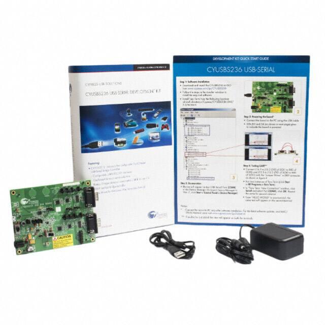
The CYUSBS236 kit contains the following items:
■
CYUSBS236 DVK board
■
Quick start guide
■
USB standard-A to micro-B cable
■
Jumper wires
■
Extra jumpers
■
5-V power supply adapter
■
CY7C65215-32LTXI sample silicon chips
CYUSBS236 USB-Serial Development Kit Guide, Doc. # 001-86996 Rev. **
7
�Introduction
Figure 1-1. Kit Contents
Inspect the contents of the kit; if you find any part missing, contact your nearest Cypress sales office
for assistance or go to www.cypress.com/go/support.
1.2
Getting Started
This kit guide helps you get acquainted with the CYUSBS236 DVK. The Software
Installation chapter on page 11 provides step-by-step instructions to install the CYUSBS236 DVK
software. The Kit Operation chapter on page 15 describes how the kit operates, and explains how to
configure the CY7C65215 USB-Serial bridge controller using the Cypress USB-Serial Configuration
Utility. The Hardware chapter on page 65 discusses the kit hardware. The Additional
Information chapter on page 81 explains how to run the CYUSBS236 kit on the Mac OS. The Appendix on page 83 provides the schematics, layout, bill of materials (BoM), troubleshooting guidelines,
and board layout design guidelines for the CY7C65215 USB-Serial bridge controller.
1.3
Additional Learning Resources
Visit the USB-Serial web page, www.cypress.com/go/usbserial for additional learning resources in
the form of datasheets and application notes.
1.4
Technical Support
For assistance, go to www.cypress.com/go/support or contact our customer support at +1 (800) 5414736 Ext. 8 (in the USA) or +1 (408) 943-2600 Ext. 8 (International).
CYUSBS236 USB-Serial Development Kit Guide, Doc. # 001-86996 Rev. **
8
�Introduction
1.5
1.6
Document History
Revision
PDF Creation
Date
Origin of
Change
**
09/24/2013
MVTA
Description of Change
Initial version of kit guide
Documentation Conventions
Table 1-1. Document Conventions for Guides
Convention
Usage
Courier New
Displays file locations, user entered text, and source code:
C:\ ...cd\icc\
Italics
Displays file names and reference documentation:
For example, CYUSBS236 USB DVK.cysusb.
[Bracketed, Bold]
Displays keyboard commands in procedures:
[Enter] or [Ctrl] [C]
File > Open
Represents menu paths:
File > Open > New Project
Bold
Displays commands, menu paths, and icon names in procedures:
Click the File icon and then click Open.
Times New Roman
Displays an equation:
2+2=4
Text in gray boxes
Describes cautions or unique functionality of the product.
CYUSBS236 USB-Serial Development Kit Guide, Doc. # 001-86996 Rev. **
9
�Introduction
1.7
Abbreviations
The following table lists the abbreviations used in this kit guide.
Abbreviation
Meaning
BCD
battery charger detection
CDC
communications device class
CDP
charging downstream port
CPHA
clock phase
CPOL
clock polarity
CTS
clear to send
DCD
data carrier detect
DCP
dedicated charging port
DSR
data set ready
DTR
data terminal ready
DVK
development kit
ESD
electrostatic discharge
I2C
Inter Integrated Circuit
LDO
low drop-out
PC
personal computer
PID
product ID
RI
ring indicator
RTS
request to send
SCB
serial communication block
SDP
standard downstream port
SPI
serial peripheral interface
SSN
slave select n
UART
universal asynchronous receiver transmitter
USB
universal serial bus
VID
vendor ID
CYUSBS236 USB-Serial Development Kit Guide, Doc. # 001-86996 Rev. **
10
�2.
2.1
Software Installation
CYUSBS236 DVK Software
Follow these steps to install the CYUSBS236 DVK software:
1. Download and install the CYUSBS236 DVK software from www.cypress.com/go/CYUSBS236.
The CYUSBS236 DVK software is available in two different installer formats for download:
a. CYUSBS236 Kit ISO: This file is a complete package, stored in a CD-ROM image format that
can be used to create a CD, or extract using ISO extraction programs, such as WinZip or
WinRAR. This file includes all the required software, utilities, drivers, hardware files, and user
documents.
b. CYUSBS236 Kit Setup: This installation package contains the files related to the kit. It does
not include the Windows installer, Microsoft .NET Framework, and Visual C++ redistributable
packages. If these packages are not on your computer, the installer automatically downloads
and installs them from the Internet.
2. Run cyautorun.exe to start the installation process.
3. Click Install CYUSBS236 DVK to start the installation, as shown in Figure 2-1.
Figure 2-1. Kit Installer Startup Screen
CYUSBS236 USB-Serial Development Kit Guide, Doc. # 001-86996 Rev. **
11
�Software Installation
4. Select the folder to install the CYUSBS236 DVK-related files. Choose the directory and click
Next.
Figure 2-2. Default Path for DVK Installation
5. The CYUSBS236 Kit ISO installer automatically installs the required software, if it is not present
on your computer. The CYUSBS236 Kit Setup installer directs you to download the required software from the Internet.
6. Select the installation type. The drop-down menu has two options: Typical (installs all the
required features) and Custom. Click Next after you select the installation type.
Figure 2-3. Installation Type Options
CYUSBS236 USB-Serial Development Kit Guide, Doc. # 001-86996 Rev. **
12
�Software Installation
7. Read the Cypress License Agreement and make a selection based on the terms of the license
agreement. Click Next to continue the installation.
Figure 2-4. Cypress License Agreement
8. When the installation begins, a list of packages appears on the installation page. A green check
mark appears adjacent to every package after successful installation. If a message from
Windows Security appears, accept the Always trust software from Cypress Semiconductor
option and click Install.
Figure 2-5. Installation Page
CYUSBS236 USB-Serial Development Kit Guide, Doc. # 001-86996 Rev. **
13
�Software Installation
9. Enter your contact information or select the Continue Without Contact Information check box.
Click Finish to complete the CYUSBS236 DVK installation.
Figure 2-6. CYUSBS236 DVK Installation Complete
10.After the installation is complete, the kit contents are available at the following location:
\Cypress\CYUSBS236 DVK\1.0\
2.2
Install Hardware
This kit does not require any additional hardware installation.
2.3
Uninstall Software
You can uninstall the CYUSBS236 DVK software using one of the following methods:
1. Go to Start > All Programs > Cypress > Cypress Update Manager; click the Uninstall button.
2. Go to Start > Control Panel > Programs and Features; select the program CYUSBS236 DVK
1.0 Rev. ** from the list and click the Uninstall/Change button.
CYUSBS236 USB-Serial Development Kit Guide, Doc. # 001-86996 Rev. **
14
�3.
Kit Operation
The CYUSBS236 kit demonstrates the features of the CY7C65215 USB-Serial bridge controller. The
CYUSBS236 DVK board is designed to work at 5 V. Figure 3-1 shows an image of the board with
references to the onboard components.
Figure 3-1. CYUSBS236 DVK Board
$BQ4FOTF®
#VUUPOT�#��BOE�#�
�
*$
&&130.T�6�
BOE�6�
#BUUFSZ
$IBSHFS�*$�6�
4$#��� 4FSJBM�$PNNVOJDBUJPO�#MPDL��
$POåHVSBUJPO�KVNQFST
+��
�+��
�+��
�+��
34���
-JOF�%SJWFS�6�
$:�$�����
64#�4FSJBM
%#��$POOFDUPS
+��
3FTFU�4XJUDI
48�
64#�.JDSP�#
$POOFDUPS�+�
41*�&&130.�6�
1PXFS�4XJUDI�48�
%#��$POOFDUPS
+��
1PXFS�-&%T
%��BOE�%�
(1*0�)FBEFS�+��
34���
-JOF�%SJWFS�6�
#BUUFSZ�4XJUDI�48�
%$�1PXFS�+BDL�+�
#BUUFSZ
$POOFDUPS�#)�
4$#��� 4FSJBM�$PNNVOJDBUJPO�#MPDL��
$POåHVSBUJPO�KVNQFST
+��
�+��
�+��
�+��
41*
&&130.�6��
CYUSBS236 USB-Serial Development Kit Guide, Doc. # 001-86996 Rev. **
15
�Kit Operation
3.1
Default Switch and Jumper Settings
The switches and jumpers on the CYUSBS236 DVK board are shipped with default settings for the
USB bus-powered mode, serial interface in the UART mode, CapSense, and BCD enabled. The
board is powered by the PC or the hub when it is connected by a USB standard-A to micro-B cable.
Table 3-1 provides the default configuration settings for the switches and jumpers.
Figure 3-2. Default Jumper and Switch Settings
J28 J18, J22
R63 J7, J4, J8
J17, J19, J21, J20
J29
SW1
J23
TP10 J3
SW2
J24, J26, J27, J25
Table 3-1. Default Settings
Jumper
Pins to be Shorted
SW1
Position 2–3
Power supply selection switch set to bus-powered operation
Function
SW2
Position 2–3
Battery power cut-off
J3
Open
J4
1 and 2
Battery charge enable control pin #0 (BCD0)
J7
1 and 2
Bus detect
J8
1 and 2
Battery charge enable control pin #1 (BCD1)
J17
2 and 4
SCB0 configured as UART
J18
1 and 2
SCB0 configured as UART
J19
2 and 4
SCB0 configured as UART
J20
2 and 4
SCB0 configured as UART
J21
2 and 4
SCB0 configured as UART
J22
1 and 2
J23
Open
J24
2 and 4
SCB1 configured as UART
J25
2 and 4
SCB1 configured as UART
J26
2 and 4
SCB1 configured as UART
J27
2 and 4
SCB1 configured as UART
J28
2 and 3
CapSense watershield feature disabled
J29
1 and 2
VBUS detection (The pin near R63 is pin #1 of J29)
VBAT LED
SCB0 configured as UART
GPIO header
CYUSBS236 USB-Serial Development Kit Guide, Doc. # 001-86996 Rev. **
16
�Kit Operation
3.2
USB-Serial Enumeration
The CYUSBS236 DVK board connects to the PC by a USB standard-A to micro-B cable. The board
enumerates as a composite USB device.
Follow these steps for device enumeration:
1. To power up the board:
a. Self-powered mode - Set SW1 to position 1-2 and connect the 5-V power-supply adapter to
J1 on the board.
b. Bus-powered mode - Set the switch SW1 to position 2-3.
2. Connect the USB standard-A to micro-B cable to the PC and J2 on the board.
3. The PC detects the board and the software driver is automatically bound to the USB device.
Note If the driver installation is unsuccessful, run setup.exe from the following folders with administrative privileges:
\Cypress\CYUSBS236 DVK\1.0\driver\cyusb3
\Cypress\CYUSBS236 DVK\1.0\driver\cyusbserial
For more information, refer to the Cypress USB-Serial Driver Installation Guide at the following location: \Cypress\CYUSBS236 DVK\1.0\documentation
Figure 3-3. Install Location of cyusb3 Driver
Figure 3-4. Install Location of cyusbserial Driver
Note If a "Welcome to the Found New Hardware Wizard" message appears, select the Yes, this
time only option and click Next to continue the installation.
CYUSBS236 USB-Serial Development Kit Guide, Doc. # 001-86996 Rev. **
17
�Kit Operation
4. When the software drivers are successfully bound, the board enumeration is complete. The
board appears as a composite device in the device manager of the Windows OS (to launch the
device manager in Windows 7, go to Start > Control Panel > Device Manager), as shown in
Figure 3-5.
■
USB-Serial Adapter under CypressUSBConsoleWindowsDriver
■
USB Serial Port (COM#) under Ports (COM & LPT)
■
USB-Serial (Dual Channel) Vendor MFG under Universal Serial Bus controllers
Figure 3-5. CYUSBS236 DVK Enumeration as Dual UART in Device Manager
CYUSBS236 USB-Serial Development Kit Guide, Doc. # 001-86996 Rev. **
18
�Kit Operation
3.3
USB-Serial Configuration on Windows OS
The CY7C65215 USB-Serial bridge controller supports two channel configurable UART/I2C/SPI
interfaces. Using the Cypress USB-Serial Configuration Utility, you can configure the onboard
CY7C65215 USB-Serial bridge controller as a USB-UART bridge, a USB-I2C bridge, or a USB-SPI
bridge. You can also use this utility to configure the CY7C65215 device for CapSense and BCD
functionality according to your requirements. The following sections provide detailed descriptions
about the device features and configurations.
By default, the CYUSBS236 DVK board is configured for the USB-UART bridge, CapSense, and
BCD functionality.
3.3.1
Connecting CYUSBS236 DVK to Cypress USB-Serial Configuration Utility
Follow these steps to connect the device using the Cypress USB-Serial Configuration Utility:
1. Connect the USB standard-A to micro-B cable to your PC and the J2 connector on the board.
2. Set switch SW1 to position 2-3 for bus-powered operation.
3. Run the configuration utility from Start > All Programs > Cypress > CYUSBS236 DVK > USB
Serial Configuration Utility.
For a detailed description about the configuration utility, refer to the USB-Serial Configuration Utility User Guide at the following location:
\Cypress\CYUSBS236 DVK\1.0\documentation
4. The following figure shows the startup screen of the Cypress USB-Serial Configuration Utility.
Figure 3-6. Configuration Utility Startup Screen
CYUSBS236 USB-Serial Development Kit Guide, Doc. # 001-86996 Rev. **
19
�Kit Operation
5. Click the Select Target tab. Select the device from the drop-down menu and click Connect.
Figure 3-7. Configuration Utility Select Target Tab
Note The “version” number shown in Figure 3-7 may vary depending upon the latest firmware
version on the USB-Serial bridge controller.
6. A new tab with the connected device's default settings appears, as shown in Figure 3-8. This tab
allows you to modify the device configuration settings, which can be programmed into the device.
Figure 3-8. Configuration Utility USB Tab
CYUSBS236 USB-Serial Development Kit Guide, Doc. # 001-86996 Rev. **
20
�Kit Operation
3.3.2
USB Configuration
The USB tab shows the current values of the board’s configurable USB and system parameters.
Follow these steps to view and modify the parameters for the USB configuration:
1. Follow steps 1 to 6 in the section Connecting CYUSBS236 DVK to Cypress USB-Serial
Configuration Utility on page 19 to connect the board to the Cypress USB-Serial Configuration
Utility.
2. Click the USB tab.
Figure 3-9. Configuration Utility USB Tab
3. You can configure the following USB parameters using the Cypress USB-Serial Configuration
Utility:
a. Vendor ID (VID)
b. Product ID (PID)
c. Power Mode (bus-powered or self-powered)
d. bMaxPower
e. Remote Wake-up and Suspend
f. Manufacturer string
g. Product string
h. Serial number
■
Vendor ID (VID) and Product ID (PID)
Default value: 0x04B4 and 0x0005
A 2-byte vendor ID and product ID must be set in hexadecimal format. The VID and PID options
cannot be zero or empty. The Cypress VID/PID is programmed by default. To change this,
uncheck the Use Cypress VID/PID option. Enter the VID and press the [Tab] or [Enter] key to
enable and enter the PID.
CYUSBS236 USB-Serial Development Kit Guide, Doc. # 001-86996 Rev. **
21
�Kit Operation
■
Power Mode
Default value: Bus powered
The USB power mode can be set to either self-powered or bus-powered mode.
■
bMaxPower
Default Value: 100 mA
The USB device current requirement value can be set in the range 1 to 500 mA in steps of 2 mA
units in bus-powered mode and 0 mA to 500 mA in steps of 2 mA units in self-powered mode.
■
Remote Wake-up and Suspend
Default value for Remote wake-up: Enabled
Default value for Suspend: Enabled
Default value for Power Enable: Not enabled (for this board)
Click the Configure button (next to Remote Wake-up and Suspend in the USB tab) to enable or
disable Remote wake-up and Suspend.
Figure 3-10. Remote Wake-up and Suspend Window
Configurable options:
❐
Remote wake-up: When enabled, this option can be used to wake up the USB host from suspend state remotely from the attached device. By checking the Invert Polarity box, polarity of
the wake-up pin can be inverted. On this board, J23.15 (GPIO header) is the wake-up pin. To
test the Remote wake-up functionality, follow this procedure:
a. Connect the Remote wake-up pin (J23.15) to GND (J23.16) using the provided jumper wire.
b. Connect the CYUSBS236 DVK board to a PC using a USB standard A to micro-B cable.
c. Set the PC into sleep mode. When the PC enters sleep mode, the USB host on the PC side
suspends the connected CYUSBS236 DVK board.
d. By default, the Remote wake-up pin is active high. Disconnect the Remote wake-up pin
(J23.15) from GND (J23.16) and touch TP10 (V3P3), as shown in Figure 3-2. If the Invert
Polarity option is selected, then connect the pin to GND to wake up the USB host from the
Suspend state.
❐
Suspend: By checking this box, the Suspend option is enabled. When the USB bus enters the
Suspend state, the suspend pin is asserted. By checking the Invert Polarity box, polarity of
the Suspend pin can be inverted. On this board, J23.13 (GPIO header) is the suspend pin.
❐
Power enable: The Power enable function is enabled by assigning a GPIO from the dropdown menu. When the USB-UART bridge is configured by the host, this GPIO is asserted. In
bus-powered embedded system, to meet the USB 2.0 Specification requirements during
Unconfigured and Suspend states, this pin can be used as a notification to control the power
to the system. Refer to the Configuration Utility User Guide for more details about these
options.
CYUSBS236 USB-Serial Development Kit Guide, Doc. # 001-86996 Rev. **
22
�Kit Operation
Test Procedure for Suspend and Power Enable Pin.
a. Connect the CYUSBS236 DVK board to a PC using a USB standard A to micro-B cable.
b. Set the PC into sleep mode.
c. Check the Suspend pin (J23.13) and Power Enable pin (selected GPIO which comes on
external header J23) using a digital multimeter or digital storage oscilloscope. The Suspend
pin goes low and Power Enable pin goes high during sleep mode. (By default, the invert polarity is disabled. If the invert polarity is enabled, the Suspend pin goes high during sleep mode.)
d. Wake up the PC using the Remote wake-up feature described in page 22, or using any other
device such as a mouse or keyboard connected to the PC. When the PC becomes active, the
Suspend pin goes high and power enable pin goes low.
■
Manufacturer string
Default value: Cypress Semiconductor
The Manufacturer string can be a value of up to 32 characters.
■
Product string
Default value: USB-Serial (Dual Channel)
The Product string can be a value of up to 32 characters.
■
Serial number string
Default value: NULL (No serial number)
Select the check box to enter the serial number, which can be a value of up to 32 characters. If
you do not require the serial number, deselect the check box.
System
The Configurable options are:
a. VBUS voltage is 3.3 V
b. VDDD voltage is less than 2 V
c. Enable manufacturing interface
d. I/O Level
e. I/O Mode
f. Program button
g. Disconnect button
■
VBUS voltage is 3.3 V
Default value: Unchecked
This option must be checked if the VBUS pin is supplied with 3.3 V, and unchecked if the VBUS
pin is supplied with 5 V. The board is designed only for 5-V VBUS operation. This option must
always be unchecked for the board. The CY7C65215 device supports VBUS voltage range from
3.15 V to 5.25 V.
■
VDDD voltage is less than 2 V
Default value: Unchecked
The board is designed only for 5-V operation. This option must always be unchecked for the
board. The CY7C65215 device supports VDDD voltage range from 1.71 V to 5.5 V.
■
Enable manufacturing interface
Default value: Checked
This option enables an additional vendor class manufacturing mode interface for reprogramming
the device. For more information, refer to the Enable Manufacturing Interface section in the
Cypress USB-Serial Configuration Utility User Guide.
CYUSBS236 USB-Serial Development Kit Guide, Doc. # 001-86996 Rev. **
23
�Kit Operation
■
I/O level
Default value: CMOS
You can set the device's GPIO logic levels to either CMOS or LVTTL.
■
I/O Mode
Default value: Fast
You can set the device's GPIO edge transitions to either fast or slow for EMI considerations. For
more information, refer to the GPIO AC Specifications table in the datasheet.
■
Program button
After configuring all the device settings, the updated configuration settings must be programmed
to the device. To program the device, click the Program button.
■
Disconnect button
Click this button to disconnect the DVK from the configuration utility.
4. After configuring the USB and system parameters, click the Program button to save the changed
USB parameters. On successful programming, the "Program Succeeded" message appears.
4. Click OK to continue.
5. Click the Disconnect button to disconnect the board from the configuration utility.
6. Press the reset switch SW3 on the board. The controller is reinitialized with the new parameters
and the board re-enumerates, as shown in Figure 3-5 on page 18.
CYUSBS236 USB-Serial Development Kit Guide, Doc. # 001-86996 Rev. **
24
�Kit Operation
3.3.3
UART Configuration
The CYUSBS236 DVK board is configured for two-channel UART interfaces by default. The board
can act as a dual USB-UART bridge to transfer and receive data between the device and the PC via
terminal communication software, such as Hyperterminal or Tera Term.
Follow these steps to view and modify the parameters for the UART configuration:
1. Follow steps 1 to 6 of the section Connecting CYUSBS236 DVK to Cypress USB-Serial Configuration Utility on page 19 to connect the board to the Cypress USB-Serial Configuration Utility.
2. Click the SCB0 tab. Select UART as the SCB0 mode from the drop-down menu.
Figure 3-11. Configuration Utility SCB Configuration Tab
3. Click the Configure button, as shown in Figure 3-11, to configure the UART parameters.
Figure 3-12. UART Configuration Parameters
CYUSBS236 USB-Serial Development Kit Guide, Doc. # 001-86996 Rev. **
25
�Kit Operation
You can configure the following UART parameters by using the Cypress USB-Serial Configuration
Utility:
a. Baud Rate
b. Type
c. Data Width
d. Stop Bits
e. Parity
f. Drop packets on RX error
g. Disable CTS and DSR pull-up during suspend
■
Baud Rate
Default value: 115200
You can set the baud rate for the UART in an editable drop-down combo box that lists the predefined, standard baud rates. You can also enter a specific baud rate in the combo box. The minimum and maximum baud rates supported by this board are 300 bps and 1 Mbps, respectively.
The CY7C65215 device supports 3 Mbps, but the board limits the baud rate to 1 Mbps, due to the
limitation of the RS-232 line drivers (U5 and U6).
■
Type
Default value: 6 pin for SCB0 and 4 pin for SCB1
You can set the UART type to:
a. 2 pin (RXD and TXD pins)
b. 4 pin (RXD, TXD, RTS, and CTS pins)
c. 6 pin (RXD, TXD, RTS, CTS, DSR, and DTR pins)
■
Data Width
Default value: 8 bits
You can set the UART data width to either 7 bits or 8 bits.
■
Stop Bits
Default value: 1 bit
You can set the number of UART stop bits to either 1 bit or 2 bits.
■
Parity
Default value: None
You can set the parity for the UART data transfer to either None, Odd, Even, Mark, or Space.
■
Drop packets on RX error
Default value: Unchecked
This parameter defines the behavior of the UART when an error is detected in the packet
received (RX packet/byte). When this option is selected, the data packet/byte in the RX buffer is
discarded.
■
Disable CTS and DSR pull-up during suspend
Default value: Checked
In an embedded system, this parameter can be checked to reduce system current consumption
during Suspend state. This parameter disables CTS and DSR pull-up resistors in Suspend state
to meet USB 2.0 Specification current requirements.
4. Click OK to close the Configure UART Settings window and return to the SCB0 tab.
5. Select CDC as the protocol in the drop-down menu.
CYUSBS236 USB-Serial Development Kit Guide, Doc. # 001-86996 Rev. **
26
�Kit Operation
6. Notification LEDs are set to None, by default. The notification LED pins are brought out on the
external GPIO header J23. You can configure any GPIO as a notification LED by clicking the
Configure button next to the “Notification LED” in the SCB0 tab and connect an external LED to
the assigned GPIO pin on the GPIO header J23.
7. Repeat steps 3 to 5 to configure SCB1 as UART.
Note The Enable SCB to SCB communication option is not supported on the board.
8. After configuring the UART interface, click the Program button to save the changed SCB0 and
SCB1 settings onto the controller. On successful programming, the "Program Succeeded"
message appears.
9. Click OK to continue.
10.Click the Disconnect button to disconnect the board from the configuration utility.
11. Press the reset switch SW3 on the board. The controller is reinitialized with the new parameters
and the board re-enumerates, as shown in Figure 3-13.
Figure 3-13. CYUSBS236 DVK Board Enumeration as USB-UART Controller in Device Manager
CYUSBS236 USB-Serial Development Kit Guide, Doc. # 001-86996 Rev. **
27
�Kit Operation
12.The Cypress USB-Serial Configuration Utility is displayed, as shown in Figure 3-7.
3.3.3.1
Test Procedure for CYUSBS236 DVK Configured as UART
1. To test the functionality of the UART interface, set up the jumpers as listed in Table 3-2 and
shown in Figure 3-14 and Figure 3-16.
Table 3-2. Jumper Settings
Jumper
Pins to be Shorted
Function
J17
2 and 4
SCB0_2 (Pin #28) configured for UART RTS
J18
1 and 2
SCB0_0 (Pin #2) configured for UART RXD
J19
2 and 4
SCB0_1 (Pin #27) configured for UART DSR
J20
2 and 4
SCB0_3 (Pin #29) configured for UART CTS
J21
2 and 4
SCB0_4 (Pin #30) configured for UART TXD
J22
1 and 2
SCB0_5 (Pin #3) configured for UART DTR
J24
2 and 4
SCB1_0 (Pin #5) configured for UART RXD
J25
2 and 4
SCB1_1 (Pin #6) configured for UART TXD
J26
2 and 4
SCB1_2 (Pin #7) configured for UART RTS
J27
2 and 4
SCB1_3 (Pin #8) configured for UART CTS
J29
1 and 2
VBUS selection
Figure 3-14. SCB UART Jumpers
CYUSBS236 USB-Serial Development Kit Guide, Doc. # 001-86996 Rev. **
28
�Kit Operation
Figure 3-15. SCB0 and SCB1 Jumpers
SCB0 JUMPERS
SCB1 JUMPERS
GPIO_10
GPIO_3
1
1
SPI
(MISO_IN_0)
5
2
3
Pin #28
(SCB0_2)
4
UART
(RTS#_0)
SPI
(MISO_IN_1)
J17
I2C (SCL_OUT_0)
5
2
Pin #5
(SCB1_0)
3
SPI
(MOSI_OUT_1)
1
5
2
UART
4 (RXD_1)
J24
I2C (SCL_OUT_1)
GPIO_11
GPIO_8
3
U
S
B
2
1
UART
(RXD_0)
J18
Pin #2
(SCB0_0)
S
E
R
I
A
L
GPIO_2
1
2
B
R
I
D
G
E
Pin #27
(SCB0_1)
C
O
N
T
R
O
L
L
E
R
SPI
(MOSI_OUT_0)
5
3
4
UART
(DSR#_0)
J19
SPI (SSEL_OUT_0)
GPIO_4
2
3
Pin #29
(SCB0_3)
4
Pin #6
(SCB1_1)
S
E
R
I
A
L
B
R
I
D
G
E
3
4
J25
I2C (SDA_1)
GPIO_12
1
2
Pin #7
(SCB1_2)
3
4
UART
(RTS#_1)
J26
SPI (SSEL_OUT_1)
GPIO_13
1
UART
(CTS#_0)
U
S
B
UART
(TXD_1)
J20
I2C (SDA_0)
C
O
N
T
R
O
L
L
E
R
1
2
Pin #8
(SCB1_3)
3
4
UART
(CTS#_1)
J27
SPI (SCLK_OUT_1)
GPIO_5
1
2
Pin #30
(SCB0_4)
3
GPIO_9
3
2
4
UART
(TXD_0)
J21
SPI (SCLK_OUT_0)
UART
1 (DTR#_0)
J22
Pin #3
(SCB0_5)
CYUSBS236 USB-Serial Development Kit Guide, Doc. # 001-86996 Rev. **
29
�Kit Operation
Figure 3-16. VBUS Selection Jumper
2. To check the functionality of the UART, you can perform a quick test by connecting the two DB9
connector pins with the jumper wires as follows:
❐
J15.3-J16.2 (TXD of SCB0 to RXD of SCB1)
❐
J15.2-J16.3 (RXD of SCB0 to TXD of SCB1)
❐
J15.7-J16.8 (RTS of SCB0 to CTS of SCB1)
❐
J15.8-J16.7 (CTS of SCB0 to RTS of SCB1)
Figure 3-17. Connection for Back to Back Test
CYUSBS236 USB-Serial Development Kit Guide, Doc. # 001-86996 Rev. **
30
�Kit Operation
3. Open two instances of the serial emulation terminal, such as Tera Term, which you can install
from the following location:
/Cypress/CYUSBS236 DVK/1.0/teraterm
4. In the Tera Term: New Connection window, click Serial and select USB Serial Port (COM#) as
shown in Figure 3-18. Click OK.
Note To change the UART parameters, go to Setup > Serial Port in the Tera Term terminal.
Figure 3-18. Tera Term Connection
5. Repeat step 4 for the second instance of Tera Term.
6. Type in the text on one terminal, the electrical back-to-back connection (TXD of SCB0 to RXD of
SCB1, RXD of SCB0 to TXD of SCB1) enables the data flow from SCB0 to SCB1, which is
displayed on another terminal. This test procedure validates the functioning of dual USB-UART
bridge. If the local echo option is enabled, then the entered data appears on the same terminal.
Note To enable the local echo option, go to Setup > Terminal. In the Tera "Term: Terminal
Setup" window, check the Local echo box.
Figure 3-19. Tera Term Application: Back-to-Back Test Output
Note These screenshots are captured without enabling Local echo.
3.3.3.2
Throughput Determination
Throughput is the average rate of successful data transfer over the UART channel. It is measured in
bits/second. A PC application can be used to determine the throughput of an USB-Serial bridge controller. The CY7C65215 device supports 3 Mbps, but the actual reported throughput on a PC appli-
CYUSBS236 USB-Serial Development Kit Guide, Doc. # 001-86996 Rev. **
31
�Kit Operation
cation (Tera Term) will be less than 1 Mbps, due to RS-232 line driver limitation, protocol overhead,
and PC application latency.
Follow these steps to determine the throughput of the USB-Serial bridge controller:
1. Run two instances of Tera Term.
2. In the first Tera Term window, go to Setup > Serial Port:
a. Enter ‘1000000’ in the Baud rate drop-down combo box.
b. Select Hardware in the Flow control drop-down menu.
c. Click OK
3. Go to Setup > Terminal > Receive and select CR+LF. Click OK to continue.
4. Repeat steps 2 and 3 for the second Tera Term window.
5. In the second Tera Term window, go to File menu. Select Send File from the drop-down menu, as
shown in Figure 3-20.
Figure 3-20. Sending the File
6. Select a file to be sent through USB Serial Port (COM#). After the file is selected, the data transfer starts and the window is displayed, as shown in Figure 3-21.
7. Number of bytes transferred per second determines throughput. The "Tera Term :Send File" window shows effective data throughput in Bytes/sec; multiply this value by 8 to get the throughput in
bits/sec.
Figure 3-21. Throughput Determination
CYUSBS236 USB-Serial Development Kit Guide, Doc. # 001-86996 Rev. **
32
�Kit Operation
3.3.4
I2C Configuration
You can configure the CYUSBS236 DVK board for two-channel I2C serial interface to function as a
dual USB-I2C bridge. The onboard I2C EEPROM (operating in I2C slave mode) can be connected to
the USB-Serial bridge controller, CY7C65215, to read and write data. The USB-Serial Test Utility can
be used to read, write, and verify the content of EEPROM from the PC. The Test Utility software is
available as part of the CYUSBS236 kit installer.
Follow these steps to view and modify the parameters for the I2C configuration:
1. Follow steps 1 to 6 in the section Connecting CYUSBS236 DVK to Cypress USB-Serial
Configuration Utility on page 19 to connect the board to the Cypress USB-Serial Configuration
Utility.
2. Click the SCB0 tab. Select I2C as the SCB0 mode from the drop-down menu.
Figure 3-22. SCB0 Configuration Tab
3. Click the Configure button, as shown in Figure 3-22, to configure the I2C settings.
Figure 3-23. I2C Configuration Settings
CYUSBS236 USB-Serial Development Kit Guide, Doc. # 001-86996 Rev. **
33
�Kit Operation
You can configure the following I2C parameters by using the Cypress USB-Serial Configuration
Utility:
a. Frequency
b. Mode
c. Use as wake-up source (Slave mode only)
d. Slave Address (Slave mode only)
e. Enable clock stretching (Slave mode only)
■
Frequency
Default value: 100 kHz
You can set the operating frequency of the I2C master/slave from 1 kHz to 400 kHz in the dropdown menu.
■
Mode
Default value: Master
This option is available only in I2C slave mode. USB-Serial bridge controller as I2C slave can be
used as remote wake-up source to wake-up the USB host.
You can configure the I2C mode to either a master or a slave. To use the USB-Serial bridge controller as an I2C slave, the I2C pins (SCL and SDA) of SCB0 or SCB1 should be brought out on
the external header J23. See I2C Interface on page 75 for the jumper settings to bring out these
pins on the external header J23. Connect the I2C master pins (SCL and SDA) to J23.5 (SCL) and
J23.7 (SDA) if SCB0 I2C is used. Connect the I2C master pins (SCL and SDA) to J23.2 (SCL)
and J23.4 (SDA) if SCB1 I2C is used. Refer to the Cypress USB-Serial API Documentation for
more information on establishing communication between I2C master and I2C slave (USB-Serial
bridge controller) or contact Cypress Technical Support.
■
Slave Address
Default value: 2
This option is available only in the I2C slave mode. The I2C slave address can be from 2 to 126
(in decimal) in increments of 2.
■
Enable clock stretching
Default value: Unchecked
This option is available only in I2C slave mode.
You can use this option when there is a mismatch between the master and the slave clock
frequency. Both master and slave can operate at the same frequency by enabling clock
stretching.
■
Use as wake-up source
Default value: Disabled
This option is available only in I2C slave mode. USB-Serial bridge controller as I2C slave can be
used as remote wake-up source to wake-up the USB host.
4. Click OK to close the Configure I2C Settings window and return to the SCB0 tab.
5. Select Vendor as the protocol in the drop-down menu.
6. Notification LEDs are set to None, by default for this board. The notification LED pins are brought
out on the external GPIO header J23. You can configure any GPIO as a notification LED by clicking the Configure button next to "Notification LED" in the SCB tab and connect an external LED
to the assigned GPIO pin on the GPIO header J23.
7. Repeat steps 3 to 5 to configure SCB1 as I2C.
Note The Enable SCB to SCB communication option is not supported on the board.
CYUSBS236 USB-Serial Development Kit Guide, Doc. # 001-86996 Rev. **
34
�Kit Operation
8. After configuring the I2C interface, click the Program button to save the changed SCB0 and
SCB1 settings. On successful programming, the "Program Succeeded" message appears.
9. Click OK to continue.
10.Click the Disconnect button to disconnect the board from the configuration utility.
11. Press the reset switch SW3 on the board. The controller is reinitialized with the new parameters
and the board re-enumerates, as shown in Figure 3-24.
Figure 3-24. CYUSBS236 DVK Enumeration as USB-Serial Bridge Controller in Device Manager
12.The Cypress USB-Serial Configuration Utility is displayed, as shown in Figure 3-7.
CYUSBS236 USB-Serial Development Kit Guide, Doc. # 001-86996 Rev. **
35
�Kit Operation
3.3.4.1
Test Procedure for CYUSBS236 DVK Configured as I2C
1. To test the functionality of the I2C interface, set up the jumpers as listed in Table 3-3 and shown
in Figure 3-25 and Figure 3-26.
Table 3-3. Jumper Settings
Jumper
Pins to be Shorted
Function
J17
2 and 3
SCB0_2 (Pin #28) configured for I2C SCL
J20
2 and 3
SCB0_3 (Pin #29) configured for I2C SDA
J24
2 and 3
SCB1_0 (Pin #5) configured for I2C SCL
J25
2 and 3
SCB1_1 (Pin #6) configured for I2C SDA
J29
1 and 2
VBUS selection
Figure 3-25. SCB I2C Jumpers
CYUSBS236 USB-Serial Development Kit Guide, Doc. # 001-86996 Rev. **
36
�Kit Operation
Figure 3-26. VBUS Selection
2. Run the USBSerialTestUtility from Start > All Programs > Cypress > CYUSBS236 DVK >
USBSerialTestUtility.
3. To use the default Cypress PID, change the Product ID in the text box to 000A.
Note The user has the option to enter custom Vendor ID and Product ID.
Figure 3-27. Test Utility (VID and PID Selection)
4. The test utility lists the interfaces available on the board for the I2C interface. Click OK.
CYUSBS236 USB-Serial Development Kit Guide, Doc. # 001-86996 Rev. **
37
�Kit Operation
Figure 3-28. Test Utility (change of PID)
5. The I2C[USB Port:7 - Dev Id:0] tab, which is used to test SCB0 I2C operation is displayed, as
shown in Figure 3-29.
6. Enter an EEPROM page address within the range (0x0–0xFF) specified in the text box and click
Write data. The status bar at the bottom of window displays the status of the data.
Figure 3-29. Test Utility Data Transfer
7. Click Read & verify data. When the written and read back data are the same, the "Data verification successful" message appears.
CYUSBS236 USB-Serial Development Kit Guide, Doc. # 001-86996 Rev. **
38
�Kit Operation
Figure 3-30. Test Utility Data Transfer Verification
8. Click OK. The "Data verification successful" message appears at the bottom of the window.
Figure 3-31. Test Utility Successful Data Transfer Verification
9. To test SCB1 I2C operation, click the I2C[USB Port:7 - Dev Id:1] tab, as shown in Figure 3-32.
Follow steps 6 to 8 to verify the operation.
CYUSBS236 USB-Serial Development Kit Guide, Doc. # 001-86996 Rev. **
39
�Kit Operation
Figure 3-32. Test Utility SCB1 I2C Tab
CYUSBS236 USB-Serial Development Kit Guide, Doc. # 001-86996 Rev. **
40
�Kit Operation
3.3.5
SPI Configuration
You can configure the CYUSBS236 DVK board for the two-channel SPI serial interface to function as
a dual USB-SPI bridge. The onboard SPI EEPROM (operating in the SPI slave mode) can be connected to the CY7C65215 USB-Serial bridge controller, to read and write data. The USB-Serial Test
Utility provided can be used to read, write, and verify data from the PC. The Test Utility software is
available as part of the CYUSBS236 kit installer.
Follow these steps to view and modify the parameters for the SPI configuration:
1. Follow steps 1 to 6 in the section Connecting CYUSBS236 DVK to Cypress USB-Serial
Configuration Utility on page 19 to connect the board to the Cypress USB-Serial Configuration
Utility.
2. Click the SCB0 tab. Select SPI as the SCB0 mode from the drop-down menu.
Figure 3-33. Configuration Utility SCB0 Configuration Tab
CYUSBS236 USB-Serial Development Kit Guide, Doc. # 001-86996 Rev. **
41
�Kit Operation
3. Click the Configure button, as shown in Figure 3-33, to configure the SPI settings.
Figure 3-34. SPI Configuration Settings
You can configure the following SPI parameters by using the Cypress USB-Serial Configuration
Utility:
a. Frequency
b. Data width
c. SPI mode
d. Use as wake-up source (slave mode only)
e. Protocol
f. Enable select precede (TI Protocol only)
g. CPHA and CPOL mode (Motorola Protocol only)
h. SSN Toggle mode (Motorola Protocol only)
i. Bit order
■
Frequency
Default Value: 1 MHz
You can set the SPI operating frequency from 1 kHz to 3 MHz with increments of 1 Hz.
■
Data width
Default Value: 8 bits
You can set the SPI data width from 4 bits to 16 bits in the drop-down menu.
■
SPI mode
Default value: Master
You can configure the SPI mode to either master or slave. To use USB-Serial bridge controller as
an SPI slave, the SPI pins (SSEL, SCLK, MOSI, and MISO) of SCB0 or SCB1 should be brought
out on the external header J23. See SPI Interface on page 76 for the jumper settings to bring out
these pins on the external header J23. Connect the SPI master pins (SSEL, SCLK, MOSI, and
MISO) to J23.3 (SSEL), J23.9 (SCLK), J23.7 (MOSI), and J23.5 (MISO), respectively if SCB0
SPI is used. Connect the SPI master pins (SSEL, SCLK, MOSI, and MISO) to J23.6 (SSEL),
J23.8 (SCLK), J23.4 (MOSI), and J23.2 (MISO), respectively if SCB1 SPI is used. Refer to the
Cypress USB-Serial API documentation for more information on establishing communication
between SPI master and SPI slave (USB-Serial bridge controller) or contact Cypress Technical
Support.
■
Use as Wake-up source
Default value: Disabled
CYUSBS236 USB-Serial Development Kit Guide, Doc. # 001-86996 Rev. **
42
�Kit Operation
This parameter is applicable only when the SPI mode is set to Slave.
■
Protocol
Default value: Motorola
You can select one of the three SPI protocols:
■
❐
Motorola
❐
Texas Instruments
❐
National Semiconductors
Enable Select Precede
Default status: Disabled
This parameter is applicable only when the SPI protocol is set to TI.
■
CPHA and CPOL mode
Default Value: Both Low
The CPHA (Clock Phase) and CPOL (Clock Polarity) parameters are available only when the SPI
protocol is set to Motorola.
You can set the CPOL and CPHA values to either Low or High from the drop-down menu.
■
SSN Toggle mode
Default value: Continuous
This option is available only when the SPI Protocol is set to Motorola.
You can set the SSN (Slave Select n) toggle mode to either Frame or Continuous. SPI EEPROM
on the board supports only “Continuous” SSN Toggle mode.
■
Bit Order
Default value: MSB first
You can set the bit order to either MSB first or LSB first.
Note Refer to the SPI Mode section in the Cypress USB-Serial Configuration Utility User Guide
for more information.
4. Click OK to close the Configure SPI Settings window and return to the SCB0 tab.
5. Select Vendor as the protocol in the drop-down menu.
6. Notification LEDs are set to None, by default for this board. The notification LED pins are brought
out on the external GPIO header J23. You can configure any GPIO as a notification LED by clicking the Configure button next to "Notification LED" in the SCB tab and connect an external LED
to the assigned GPIO pin on the GPIO header J23.
7. Repeat steps 3 to 5 for SCB1 configuration as SPI.
Note The Enable SCB to SCB communication option is not supported on the board.
8. After configuring the SPI interface, click the Program button to save the changed SCB0 and
SCB1 settings. On successful programming, the "Program Succeeded" message appears.
9. Click OK to continue.
10.Click the Disconnect button to disconnect the board from the configuration utility.
CYUSBS236 USB-Serial Development Kit Guide, Doc. # 001-86996 Rev. **
43
�Kit Operation
11. Press the reset switch SW3 on the board. The controller is reinitialized with the new parameters
and the board re-enumerates, as shown in Figure 3-35.
Figure 3-35. CYUSBS236 DVK Enumeration as USB-Serial Bridge Controller in Device Manager
12.The Cypress USB-Serial Configuration Utility is displayed, as shown in Figure 3-7 on page 20.
CYUSBS236 USB-Serial Development Kit Guide, Doc. # 001-86996 Rev. **
44
�Kit Operation
3.3.5.1
Test Procedure for CYUSBS236 DVK Configured as SPI
1. To test the functionality of the SPI interface, set up the jumpers as listed in Table 3-4 and shown
in Figure 3-36 and Figure 3-37.
Table 3-4. Jumper Settings
Jumper
Pins to be Shorted
Function
J17
2 and 5
SCB0_2 (Pin #28) configured for SPI MISO
J19
2 and 3
SCB0_1 (Pin #27) configured for SPI SSEL
J20
2 and 5
SCB0_3 (Pin #29) configured for SPI MOSI
J21
2 and 3
SCB0_4 (Pin #30) configured for SPI SCLK
J24
2 and 5
SCB1_0 (Pin #5) configured for SPI MISO
J25
2 and 5
SCB1_1 (Pin #6) configured for SPI MOSI
J26
2 and 3
SCB1_2 (Pin #7) configured for SPI SSEL
J27
2 and 3
SCB1_3 (Pin #8) configured for SPI SCLK
J29
1 and 2
VBUS selection
Figure 3-36. SCB SPI Jumpers
CYUSBS236 USB-Serial Development Kit Guide, Doc. # 001-86996 Rev. **
45
�Kit Operation
Figure 3-37. VBUS Selection
2. Run the USBSerialTestUtility from Start > All Programs > Cypress > CYUSBS236 DVK >
USBSerialTestUtility.
3. To use the default Cypress PID, change the Product ID in the text box to ‘000A’.
Note The user has the option to enter custom Vendor ID and Product ID.
Figure 3-38. Test Utility (VID and PID Selection)
4. The test utility lists the interfaces available on the board for the SPI interface. Click OK.
CYUSBS236 USB-Serial Development Kit Guide, Doc. # 001-86996 Rev. **
46
�Kit Operation
Figure 3-39. Test Utility (PID Change)
5. The SPI[USB Port:7 - Dev Id:0] tab, which is used to test SCB0 SPI operation is displayed, as
shown in Figure 3-40.
6. Enter an EEPROM page address within the range specified in the text box (0x0–0x3FF) and click
the Write data button. The status bar at the bottom of the window displays the status of the write
data operation.
Figure 3-40. Test Utility Data Transfer
CYUSBS236 USB-Serial Development Kit Guide, Doc. # 001-86996 Rev. **
47
�Kit Operation
7. Click Read & verify data. When the data that is written and read back are identical, a data verification successful message appears.
Figure 3-41. Test Utility Data Transfer Verification
8. Click OK. The "Data Verification successful" message appears at the bottom of the window.
Figure 3-42. Test Utility Successful Data Transfer
9. To test SCB1 SPI operation, click the SPI[USB Port:7 - Dev Id:1] tab, as shown in Figure 3-43.
Follow steps 6 to 8 to verify the operation.
CYUSBS236 USB-Serial Development Kit Guide, Doc. # 001-86996 Rev. **
48
�Kit Operation
Figure 3-43. Test Utility SCB1 SPI Tab
CYUSBS236 USB-Serial Development Kit Guide, Doc. # 001-86996 Rev. **
49
�Kit Operation
3.3.6
CapSense Configuration
The CY7C65215 USB-Serial bridge controller supports the configurable CapSense functionality, providing best-in-class signal-to-noise ratio (SNR) and water tolerance. This device supports
SmartSense™ Auto-Tuning of the CapSense parameters and does not require manual tuning.
SmartSense Auto-tuning compensates for printed circuit board (PCB) variations and device process
variations. The CYUSBS236 DVK board has two CapSense buttons to evaluate the CapSense functionality.
Follow these steps to view and modify the parameters for the CapSense configuration:
1. Follow steps 1 to 6 in the section Connecting CYUSBS236 DVK to Cypress USB-Serial Configuration Utility on page 19 to connect the board to the Cypress USB-Serial Configuration Utility.
2. Click the CapSense®/BCD/GPIO tab. Click the Configure button next to Enable/Disable
CapSense®.
Figure 3-44. CapSense/BCD/GPIO Configuration Tab
CYUSBS236 USB-Serial Development Kit Guide, Doc. # 001-86996 Rev. **
50
�Kit Operation
3. To enable the CapSense functionality, check the Enable CapSense option. Set Buttons Needed
to 2, because this board supports two CapSense buttons denoted as B1 assigned to GPIO 06
and B2 assigned to GPIO 07. Assign these GPIOs to Input Sense GPIO from the drop-down
menu adjacent to Button 1 and Button 2, as shown in Figure 3-45.
Figure 3-45. CapSense Configuration Editor
You can configure the following CapSense parameters by using the Cypress USB-Serial Configuration Utility:
a. Enable CapSense
b. Use as wake-up source
c. Debounce
d. Scan Rate
e. Water Shield
f. Output activity LED
g. Buttons needed
h. Input Sense GPIO
i. Activity LED GPIO
j. Sensitivity
k. Select encoded output GPIO
l. Auto Assign (Not applicable to this board)
■
Enable CapSense
Check this box to enable the CapSense block in the device.
■
Use as wake-up source
Check this box to wake up the USB-Serial bridge controller from low-power mode when the
CapSense button is touched.
CYUSBS236 USB-Serial Development Kit Guide, Doc. # 001-86996 Rev. **
51
�Kit Operation
■
Debounce
Default Value: 1
Debounce value defines the number of scan cycles (scan rate x number of buttons) a button
press needs to be detected by the device before a button press status is reported. For example, if
the debounce value is set to two, the device reports a button press status only when it detects the
button press for two continuous scan cycles.
Debounce ensures that high-frequency high-amplitude noise does not cause false detection of a
pressed button. The debounce value can be set to any value between 1 and 5. By default, the
debounce value is set to 1.
■
Scan rate
Default value: 1 ms
Scan rate is the delay (in ms) between two button scans. For example, if the device has three
CapSense buttons and scan rate set to 2 ms, each button will be scanned once every 6 ms.
Scan rate can be set to any value between 1 ms and 5 ms. By default, the scan rate is set to
1 ms.
■
Water shield
Default value: Disabled
You can enable the waterproofing feature by selecting any GPIO from the drop-down menu.
When this feature is enabled, water droplets on the CapSense button will not be considered as
finger touch. The waterproofing design uses a concept called “shield”, which is a conductor
placed around the sensors and is connected to a designated shield pin on the device. The shield
must be connected to ground by setting jumper J28 to position 2-3 when not used. In the
CYUSBS236 board, GPIO 01 is used for water shield operation and the recommended value of
sensitivity is 0.2 pF for waterproofing operation. Set the jumper J28 to position 1-2 to test the
waterproofing operation.
■
Output activity LED
Default value: None
The output activity LED is an indicator for CapSense button touch. You can configure the LED for
no indication by setting it to None; one LED for every button by setting it to Individual; or a common LED for more than one CapSense button.
■
Buttons Needed
Default value: 2
This option defines the number of buttons required for a CapSense operation. This device
supports eight buttons but the board supports two CapSense buttons.
■
Input Sense GPIO
This option assigns the GPIO to a CapSense button. On this board, CapSense is assigned to
GPIO 06 for button B1 and GPIO 07 for button B2.
■
Activity LED GPIO
Default value: None
This option assigns the GPIO used for the LED indication of the CapSense function. The LED will
glow when the assigned CapSense button is touched. On this board, the LEDs are assigned to
GPIO 14 and GPIO 15.
■
Sensitivity
Default value: 0.2 pF
This option selects the sensitivity of the CapSense button to detect finger touch. You can set the
sensitivity to a value between 0.1 pF to 0.4 pF in increments of 0.1 pF. The recommended value
for this board is 0.2 pF.
CYUSBS236 USB-Serial Development Kit Guide, Doc. # 001-86996 Rev. **
52
�Kit Operation
■
Select encoded output GPIO
This option selects the GPIOs that generate a binary-encoded output for an assigned CapSense
button. On this board, the encoded output is assigned to GPIO 14 for B1 and GPIO 15 for B2.
■
Auto assign
This option automatically assigns the GPIOs from the available free pool of GPIOs.
4. Click OK to close the Configure CapSense® window and return to the CapSense®/BCD/GPIO
tab.
5. After configuring CapSense, click the Program button to save the changed CapSense settings.
On successful programming, the "Program Succeeded" message appears.
6. Click OK to continue.
7. Click the Disconnect button to disconnect the board from the configuration utility.
8. Press the reset switch SW3 on the board. The controller is reinitialized with the new parameters
and the board re-enumerates, as shown in Figure 3-46.
Figure 3-46. USB-Serial Bridge Controller Enumeration in Device Manager
9. The Cypress USB-Serial Configuration Utility is displayed, as shown in Figure 3-7.
CYUSBS236 USB-Serial Development Kit Guide, Doc. # 001-86996 Rev. **
53
�Kit Operation
3.3.6.1
Test Procedure for CYUSBS236 DVK Configured for CapSense
1. To test the functionality of the CapSense, set up the jumper as listed in Table 3-5 and shown in
Figure 3-47 and Figure 3-48.
Table 3-5. Jumper Settings
Jumper
Pins to be Shorted
Function
J28
2 and 3
Waterproofing disabled—Shield is connected to GND
J29
1 and 2
VBUS selection
Figure 3-47. CapSense Jumper (Waterproofing Disabled)
Figure 3-48. VBUS Selection
2. On the board, press the CapSense button B1; the LED D7 glows. Now, press button B2; LED
D12 glows.
CYUSBS236 USB-Serial Development Kit Guide, Doc. # 001-86996 Rev. **
54
�Kit Operation
3. If you touch both buttons B1 and B2 simultaneously, then LED output depends upon the
configuration as follows:
a. Case 1 (Default Configuration):
Output activity LED and Activity LED GPIO are set to None.
Select encoded output GPIOs are set to GPIO 14 for B1 and GPIO 15 for B2.
With this configuration, LED D7 glows. This is because B1 gets higher priority than B2 as multitouch output is not supported in this configuration.
b. Case 2 (Custom Configuration):
Output activity LED is set to Individual.
Activity LED GPIO is set to GPIO 14 for B1 and GPIO 15 for B2.
Select encoded output GPIOs are set to available free GPIOs.
With this configuration, both LEDs D7 and D12 glow. Multitouch output is supported in this
configuration.
4. To validate CapSense using the Cypress USB-Serial Configuration Utility, follow these steps:
❐
Click the Launch button next to Validate CapSense®.
Figure 3-49. CapSense Validation
❐
Select the Button Specific Validation view from the drop-down menu and click the Load
view button.
CYUSBS236 USB-Serial Development Kit Guide, Doc. # 001-86996 Rev. **
55
�Kit Operation
Figure 3-50. CapSense Button-specific Validation
❐
Select 1 for B1 and 2 for B2 from the drop-down menu against Select Button. Select the
RAW count vs Baseline graph from the drop-down menu. For more information about the
options in this window, refer to the Configuration Utility User Guide.pdf.
❐
The CapSense validation window displays a blue line, which indicates the raw counts without
finger touch called the “baseline”. During this event, the button status is OFF.
Figure 3-51. Raw Counts Without Finger Touch
CYUSBS236 USB-Serial Development Kit Guide, Doc. # 001-86996 Rev. **
56
�Kit Operation
❐
Touch button B1 with a finger. The CapSense validation window displays a red line, which
indicates the raw counts. During this event, the button status is ON.
Figure 3-52. CapSense Finger Touch Output
CYUSBS236 USB-Serial Development Kit Guide, Doc. # 001-86996 Rev. **
57
�Kit Operation
3.3.7
Battery Charger Detection (BCD) Configuration
The battery charger detection logic in the CY7C65215 device will detect the source of power on the
USB port and provides indication over the BCD0 and BCD1 GPIOs.
Follow these steps to view and modify the parameters for BCD configuration:
1. Follow steps 1 to 6 in the section Connecting CYUSBS236 DVK to Cypress USB-Serial
Configuration Utility on page 19 to connect the board to the Cypress USB-Serial Configuration
Utility.
2. Click the CapSense®/BCD/GPIO tab. Click the Configure button next to Battery Charge Detect
(BCD) to launch the Configure BCD window.
Figure 3-53. CapSense/BCD/GPIO Configuration Tab
CYUSBS236 USB-Serial Development Kit Guide, Doc. # 001-86996 Rev. **
58
�Kit Operation
3. To enable the BCD functionality, check the Enable BCD option. In the board, GPIO 18, GPIO 16,
and GPIO 17 are configured as BCD0, BCD1, and Bus Detect pins, respectively. Assign these
GPIOs to BCD0, BCD1, and Bus Detect pins, as shown in Figure 3-54.
Figure 3-54. BCD Configuration Settings
Note The dead/no battery condition is not supported by the CY7C65215 USB-Serial bridge
controller.
Configuring the BCD1 and BCD0 drive mode to High in the BCD mode is not a valid condition for
this board. If this condition is enabled, the battery charger IC enters into the Suspend mode.
You can configure the following BCD parameters by using the Cypress USB-Serial Configuration
Utility:
a. Enable BCD
b. BCD0
c. BCD1
d. Bus Detect
e. BCD Drive mode
■
Enable BCD
Check this option to enable the BCD block in the device.
■
BCD0 and BCD1
You can assign GPIOs to BCD0 and BCD1 from the drop-down menu according to the requirements of the battery charging IC (refer to the battery charging IC datasheet for the truth table).
■
Bus Detect
The Bus Detect pin is used to detect the presence of 5 V on VBUS. You must assign a GPIO to
the Bus Detect pin from the drop-down menu to detect the USB connection.
■
BCD Drive mode
The board has a battery charging IC to charge the Li-Ion battery (not included) at various levels,
based on the status of BCD0 and BCD1. A truth table must be designed to meet the battery
charging current drawn by the battery-charging IC, depending on the source of the USB power.
The battery-charging IC, MAX8856, on the board sets the charging current, as provided in truth
table in Table 3-6.
CYUSBS236 USB-Serial Development Kit Guide, Doc. # 001-86996 Rev. **
59
�Kit Operation
Table 3-6. BCD Drive Mode Truth Table
BCD0/EN1#
BCD1/EN2#
MODE
0
0
100 mA
0
1
500 mA
1
0
750 mA
1
1
Suspend
Note Depending on the battery-charging IC that you select, the truth table provided in Table 3-6
will change. You must select a battery-charging IC with two control pins to interface with the USBSerial bridge controller.
4. Click OK to close the Configure BCD window and return to the CapSense®/BCD/GPIO tab.
5. After configuring the BCD, click the Program button to save the changed BCD settings. On successful programming, the "Program Succeeded" message appears.
6. Click OK to continue.
7. Click the Disconnect button to disconnect the board from the configuration utility.
3.3.7.1
Test Procedure for CYUSBS236 DVK Configured for BCD
1. To test the functionality of the BCD, set up the jumpers as listed in Table 3-7 and shown in
Figure 3-55 and Figure 3-56.
Table 3-7. Jumper Settings
Jumper
Pins to be Shorted
Function
J4
1 and 2
Battery charge enabled - BCD0
J7
1 and 2
Bus detect
J8
1 and 2
Battery charge enabled - BCD1
J29
1 and 2
VBUS Selection
Figure 3-55. BCD Jumpers
CYUSBS236 USB-Serial Development Kit Guide, Doc. # 001-86996 Rev. **
60
�Kit Operation
Figure 3-56. VBUS Selection
2. Press the reset switch SW3 on the board. The controller is reinitialized with the new parameters
and the board re-enumerates as shown in Figure 3-57.
Figure 3-57. USB-Serial Bridge Controller Enumeration in Device Manager
3. The Cypress USB-Serial Configuration Utility is displayed, as shown in Figure 3-7.
WARNING The SW2 switch should be in position 2-3 before connecting the battery. Use only the
recommended rechargeable Li-ion battery. Check the polarity of the battery connector before
connecting to the board.
4. Connect a rechargeable Li-ion battery (not supplied with the board) to the battery connector BH1.
This board has been tested with a Tenergy Li-Ion 18650 3.7V 2600 mAh rechargeable battery
(MPN: 30011-02).
5. Set SW2 in position 1-2.
6. The battery will charge when its voltage is below the nominal voltage (3.7 V), which is indicated
by the LED D5.
Note The Li-Ion battery is not provided with the CYUSBS236 DVK board.
7. Set the SW2 switch to position 2-3 and disconnect the battery.
CYUSBS236 USB-Serial Development Kit Guide, Doc. # 001-86996 Rev. **
61
�Kit Operation
3.3.8
CYUSBS236 DVK Restore Default Configuration Settings
The CYUSBS236 DVK board features the CY7C65215 USB-Serial bridge controller, which is factory-programmed for dual USB-UART bridge, CapSense, and BCD functionalities. You can reconfigure the device using the Cypress USB-Serial Configuration Utility to meet specific requirements that
overwrites the factory configuration.
To restore the board to the factory settings, follow these steps:
1. Follow steps 1 to 6 in the section Connecting CYUSBS236 DVK to Cypress USB-Serial
Configuration Utility on page 19 to connect the board to the Cypress USB-Serial Configuration
Utility.
2. Click File > Open Configuration from > Disk, as shown in Figure 3-58.
Figure 3-58. Select Configuration Window
Note The "Restore Default Settings" option will restore the silicon's default settings, which is different from the
board default settings.
CYUSBS236 USB-Serial Development Kit Guide, Doc. # 001-86996 Rev. **
62
�Kit Operation
3. Select the default configuration file from the following location:
\Cypress\CYUSBS236 DVK\1.0\default factory
settings\CYUSBS236 USB DVK.cyusb
Figure 3-59. Select Default Configuration File Window
4. After successfully loading the configuration file, the message “Configuration settings were
successfully loaded from the file” appears. Click OK to continue.
Figure 3-60. Load Configuration
CYUSBS236 USB-Serial Development Kit Guide, Doc. # 001-86996 Rev. **
63
�Kit Operation
5. Click Program to update the configuration settings. On successful programming, the "Program
Succeeded” message appears.
6. Click OK to continue.
7. Click Disconnect to disconnect the board from the configuration utility and press the reset switch
SW3 on the board.
8. The Cypress USB-Serial Configuration Utility is displayed as shown in Figure 3-7; the board enumerates as shown in Figure 3-5.
CYUSBS236 USB-Serial Development Kit Guide, Doc. # 001-86996 Rev. **
64
�4.
4.1
Hardware
Board Details
The CYUSBS236 DVK board consists of the following components:
■
CY7C65215 USB-Serial bridge controller
■
Power-supply system
■
USB connector
■
Two serial communication blocks
❐
SCB0 and SCB1 jumpers
❐
Two RS-232 line drivers for UART interfaces
❐
Two I2C EEPROMs for I2C interfaces
❐
Two SPI EEPROMs for SPI interfaces
❐
GPIO Header
■
Two CapSense buttons
■
Li-Ion battery charger
■
Reset switch
■
LEDs
Figure 4-1. CYUSBS236 DVK Board
$BQ4FOTF®
#VUUPOT�#��BOE�#�
*�$
&&130.T�6�
BOE�6�
#BUUFSZ
$IBSHFS�*$�6�
4$#��� 4FSJBM�$PNNVOJDBUJPO�#MPDL��
$POåHVSBUJPO�KVNQFST
+��
�+��
�+��
�+��
34���
-JOF�%SJWFS�6�
$:�$�����
64#�4FSJBM
%#��$POOFDUPS
+��
3FTFU�4XJUDI
48�
64#�.JDSP�#
$POOFDUPS�+�
41*�&&130.�6�
1PXFS�4XJUDI�48�
%#��$POOFDUPS
+��
1PXFS�-&%T
%��BOE�%�
(1*0�)FBEFS�+��
34���
-JOF�%SJWFS�6�
#BUUFSZ�4XJUDI�48�
%$�1PXFS�+BDL�+�
#BUUFSZ
$POOFDUPS�#)�
4$#��� 4FSJBM�$PNNVOJDBUJPO�#MPDL��
$POåHVSBUJPO�KVNQFST
+��
�+��
�+��
�+��
41*
&&130.�6��
CYUSBS236 USB-Serial Development Kit Guide, Doc. # 001-86996 Rev. **
65
�Hardware
4.2
Theory of Operation
This section provides the block-level description of the CYUSBS236 DVK board.
Figure 4-2. Hardware Block Diagram
RESET
DC
Power
Jack(J1)
DC
Regulator
UART
DP
DM
VBUS
Micro B
USB
Connector
(J2)
LEVEL
TRANSLATOR
USB
SCB0
JUMPER
SELECTOR
I2C
SPI
CY7C65215
LI-ION
Battery
Battery
Charger
IC
BCD
I2C
EEPROM
SPI
EEPROM
UART
LEVEL
TRANSLATOR
B1
SCB1
JUMPER
SELECTOR
I2C
DB9
Connector
(J15)
DB9
Connector
(J16)
I2C
EEPROM
CAPSENSE
SPI
B2
SPI
EEPROM
The CY7C65215 is a full-speed USB-Serial bridge controller that offers two configurable serial
channels for UART/I2C/SPI interface. This device also integrates the industry-leading CapSense
technology (for touch-sensitive key switches) and the USB-IF Battery Charging specification ver. 1.2
(to detect the power source on the USB port). This device is a fixed-function controller, which does
not require any changes to the firmware on the embedded products, because the parameters of the
controller and serial channels can be modified using an easy-to-use Cypress USB-Serial
Configuration Utility.
The CYUSBS236 DVK board communicates through the USB to configure the CY7C65215 USBSerial bridge controller. The board can function as a dual USB to UART/I2C/SPI bridge. This board
also showcases the CapSense and BCD functionalities. The board has two RS-232 line drivers, two
I2C EEPROMs, and two SPI EEPROMs to demonstrate the USB-UART, USB-I2C, and USB-SPI
bridge functionalities respectively. This board has a set of jumpers that must be configured according
to the UART/I2C/SPI functionality. For more information about the jumpers, see SCB0 and SCB1
Jumpers on page 71. The board has a reset switch, which connects to the XRES pin of the
CY7C65215 USB-Serial bridge controller and touch-sensitive buttons to demonstrate CapSense.
This board also has a battery-charging IC to charge the Li-ion battery, which is connected to the battery connector to demonstrate BCD.
You can power the board from a USB standard-A to micro-B cable, DC power supply, or battery. This
board is designed to work at 5 V. The board has two switches; switch SW1 is used to select either
self-powered or bus-powered mode and switch SW2 is used to connect the external Li-ion battery to
the battery charging circuit.
CYUSBS236 USB-Serial Development Kit Guide, Doc. # 001-86996 Rev. **
66
�Hardware
4.3
Functional Description
This DVK uses the CY7C65215 full-speed USB controller that enables seamless PC connectivity for
peripherals with two-channel serial interfaces, such as UART, SPI, and I2C. CY7C65215 also integrates CapSense and BCD-compliant with the USB Battery Charging Specification, Rev. 1.2. It integrates a voltage regulator, an oscillator, and flash memory for storing configuration parameters,
offering a cost-effective solution. The CY7C65215 device supports bus-powered and self-powered
modes and enables efficient system power management with suspend and remote wake-up signals.
It is available in a 32-pin QFN package. For more information, refer to the USB-Serial web page at
www.cypress.com/go/usbserial and the USB-Serial datasheet.
4.3.1
Features
■
■
USB 2.0-certified, Full-Speed (12 Mbps)
❐
Supports communication driver class (CDC), personal health care device class (PHDC), and
vendor-specific drivers
❐
BCD compliant with USB Battery Charging Specification, Rev. 1.2 (Peripheral Detect only)
❐
Integrated USB termination resistors
Two-channel configurable UART interface
❐
Data rates up to 3 Mbps
❐
256 bytes for each transmit and receive buffer
❐
Data format:
7 to 8 data bits
1 to 2 stop bits
■
■
■
❐
No parity, even, odd, mark, or space parity
❐
Supports parity, overrun, and framing errors
❐
Supports flow control using Clear To Send (CTS), Request To Send (RTS), Data Terminal
Ready (DTR), Data Set Ready (DSR)
Two-channel configurable SPI interface
❐
Master/slave up to 3 MHz
❐
Data width: 4 bits to 16 bits
❐
256 bytes for each transmit and receive buffer
❐
Supports Motorola, TI, and National Semiconductor SPI modes
Two-channel configurable I2C interface
❐
Master/slave up to 400 kHz
❐
256 bytes each transmit and receive buffer
❐
Supports multi-master I2C
CapSense
❐
SmartSense Auto-tuning enabled
CYUSBS236 USB-Serial Development Kit Guide, Doc. # 001-86996 Rev. **
67
�Hardware
4.3.2
Power-Supply System
The power-supply system on this board is designed to be powered-up from one of the following input
sources:
■
External 5-V DC power supply (self-powered operation)
■
Power from USB bus (bus-powered operation)
■
Battery power supply
The USB-Serial bridge controller on this board is powered by 3.3 V. The onboard Low Drop Out regulator provides the required 3.3 V, with input from one of the above sources.
■
■
■
The board is powered by 5-V DC power supply when:
❐
5-V DC power supply is plugged in DC power jack (J1)
❐
SW1 is set to position 1-2
❐
SW2 can be set to any position
The board is powered by USB power supply when:
❐
USB standard-A to micro-B cable is plugged in micro-B connector(J2)
❐
SW1 is set to position 2-3
❐
SW2 can be set to any position
The board is powered from the battery power supply when:
❐
Li-ion rechargeable battery is connected in BH1 connector.
❐
SW2 is set to position 1-2
❐
SW1 is set to position 2-3
VBUS
L3
Battery
Charger
IC
DC
Power
Jack
Switch
(SW1)
USB
Figure 4-3. Power Supply Block Diagram
D1
MAX3245
Switch
(SW2)
LDO
3.3V
MAX3245
CY7C65215
I2C
EEPROM
I2C
EEPROM
SPI
EEPROM
SPI
EEPROM
CYUSBS236 USB-Serial Development Kit Guide, Doc. # 001-86996 Rev. **
68
�Hardware
4.3.3
LEDs
The CYUSBS236 DVK board has nine LEDs. D2 and D4 LEDs indicate the power status. D7 and
D12 LEDs indicate the CapSense finger touch on buttons B1 and B2, the D5 LED indicates battery
charging operation, D8 and D10 LEDs indicate the activity on the TXD and RXD lines of the SCB0
UART, and D9 and D11 LEDs indicate the activity on the TXD and RXD lines of the SCB1 UART.
Figure 4-4. LED D2 (5-V Power On Indication)
Figure 4-5. LED D4 (3.3-V Power-on Indication)
Figure 4-6. LED D5 (Battery Charging Indication)
Figure 4-7. LED D7 and D12 (CapSense Touch Indication)
CYUSBS236 USB-Serial Development Kit Guide, Doc. # 001-86996 Rev. **
69
�Hardware
Figure 4-8. LEDs D8 and D10 (TXD and RXD Activity Indication for UART Port SCB0)
Figure 4-9. LEDs D9 and D11 (TXD and RXD Activity Indication for UART Port SCB1)
4.3.4
USB Connector
A USB standard micro-B connector is used on the board. The shield of this USB connector is
connected to the ground and two inductors (L3 and L4) are placed on VBUS and GND pins to
reduce the noise from power supply lines. ESD protection is provided on the D+, D–, and VBUS
lines.
CYUSBS236 USB-Serial Development Kit Guide, Doc. # 001-86996 Rev. **
70
�Hardware
Figure 4-10. USB Connector
4.3.5
Serial Communication Block (SCB)
The CY7C65215 USB-Serial bridge controller integrates two SCB blocks that can be configured for
UART, I2C or SPI interfaces. The board incorporates RS-232 line drivers (U5 and U6), and DB-9
connectors (J15 and J16) to evaluate the UART functionality. EEPROMs (U7 and U9) and
EEPROMs (U8 and U10) are used to evaluate the I2C and SPI functionalities on the CYUSBS236
DVK board. As an option, these onboard devices can be disconnected using SCB0 and SCB1 jumpers and the serial interface signals can be made available on header J23 for external connectivity.
4.3.5.1
SCB0 and SCB1 Jumpers
This board has six SCB0 jumpers (J17, J18, J19, J20, J21, and J22) and four SCB1 jumpers (J24,
J25, J26, and J27). These jumpers must be configured for USB to UART/I2C/SPI operation. These
jumpers are grouped as 3/4/5 pins configurations. Table 4-1 and Table 4-2 provides the jumper
configuration details.
CYUSBS236 USB-Serial Development Kit Guide, Doc. # 001-86996 Rev. **
71
�Hardware
Table 4-1. Jumper Configuration for SCB0 (UART/I2C/SPI/GPIO)
J17
J18
J19
J20
J21
J22
UART
2–4
2–1
2–4
2–4
2–4
2–1
I2C
2–3
SPI
2–5
GPIO HEADER
2–1
2–3
2–3
2–1
2–5
2–3
2–1
2–1
2–3
Table 4-2. Jumper Configuration for SCB1 (UART/I2C/SPI/GPIO)
J24
J25
J26
J27
UART
2–4
2–4
2–4
2–4
I2C
2–3
2–3
SPI
2–5
2–5
2–3
2–3
GPIO HEADER
2–1
2–1
2–1
2–1
Figure 4-11. SCB0 and SCB1 Jumpers
SCB0 JUMPERS
SCB1 JUMPERS
GPIO_10
GPIO_3
1
1
SPI
(MISO_IN_0)
5
2
3
Pin #28
(SCB0_2)
4
UART
(RTS#_0)
SPI
(MISO_IN_1)
J17
I2C (SCL_OUT_0)
5
2
Pin #5
(SCB1_0)
3
SPI
(MOSI_OUT_1)
1
5
2
UART
4 (RXD_1)
J24
I2C (SCL_OUT_1)
GPIO_11
GPIO_8
3
U
S
B
2
1
UART
(RXD_0)
J18
Pin #2
(SCB0_0)
S
E
R
I
A
L
GPIO_2
1
2
B
R
I
D
G
E
Pin #27
(SCB0_1)
C
O
N
T
R
O
L
L
E
R
SPI
(MOSI_OUT_0)
5
3
4
UART
(DSR#_0)
J19
SPI (SSEL_OUT_0)
GPIO_4
2
3
Pin #29
(SCB0_3)
4
Pin #6
(SCB1_1)
S
E
R
I
A
L
B
R
I
D
G
E
3
UART
(TXD_1)
J25
I2C (SDA_1)
GPIO_12
1
2
Pin #7
(SCB1_2)
3
4
UART
(RTS#_1)
J26
SPI (SSEL_OUT_1)
GPIO_13
1
UART
(CTS#_0)
U
S
B
4
J20
I2C (SDA_0)
C
O
N
T
R
O
L
L
E
R
1
2
Pin #8
(SCB1_3)
3
4
UART
(CTS#_1)
J27
SPI (SCLK_OUT_1)
GPIO_5
1
2
Pin #30
(SCB0_4)
3
GPIO_9
3
2
4
UART
(TXD_0)
J21
SPI (SCLK_OUT_0)
UART
1 (DTR#_0)
J22
Pin #3
(SCB0_5)
CYUSBS236 USB-Serial Development Kit Guide, Doc. # 001-86996 Rev. **
72
�Hardware
4.3.5.2
RS-232 Interface
This board has two RS-232 line drivers and two DB9 connectors for the RS-232 interfaces, with a
maximum baud rate of 1 Mbps (limited by RS-232 line driver). The board includes two LED indicators for RXD (D10 for SCB0 and D11 for SCB1) and TXD (D8 for SCB0 and D9 for SCB1) activity for
each RS-232 interface.
Figure 4-12. RS-232 Interface (SCB0)
CYUSBS236 USB-Serial Development Kit Guide, Doc. # 001-86996 Rev. **
73
�Hardware
Figure 4-13. RS-232 Interface (SCB1)
CYUSBS236 USB-Serial Development Kit Guide, Doc. # 001-86996 Rev. **
74
�Hardware
4.3.5.3
I2C Interface
The CY7C65215 USB-Serial bridge controller's SCB0 and SCB1 pins can be configured for I2C.
These pins are brought out on jumpers (J17 and J20 for SCB0 and J24 and J25 for SCB1) to provide
I2C interface. The board has dedicated I2C slave EEPROMs to evaluate the I2C interface. The
CY7C65215 USB-Serial bridge controller is configured as an I2C master. The I2C pins (SCL and
SDA) of SCB0 can be brought out on the external header J23 by putting the jumper on position 1-2
of J17 and J20. The I2C pins (SCL and SDA) of SCB1 can be brought out on the external header
J23 by putting the jumper on position 1-2 of J24 and J25.
Figure 4-14. I2C Interface (SCB0 and SCB1)
CYUSBS236 USB-Serial Development Kit Guide, Doc. # 001-86996 Rev. **
75
�Hardware
4.3.5.4
SPI Interface
The CY7C65215 USB-Serial bridge controller's SCB0 and SCB1 pins can be configured for SPI.
These pins are brought out on jumpers (J17, J19, J20, and J21 for SCB0 and J24, J25, J26, and J27
for SCB1) to provide the SPI interface. The board has dedicated SPI slave EEPROMs to evaluate
the SPI interface. The CY7C65215 USB-Serial bridge controller is configured as a SPI master. The
SPI pins (SSEL, MISO, MOSI, and SCLK) of SCB0 can be brought out on the external header J23
by putting the jumper on position 1-2 of J17, J19, J20, and J21. The SPI pins (SSEL, MISO, MOSI,
and SCLK) of SCB1 can be brought out on the external header J23 by putting the jumper on position
1-2 of J24, J25, J26, and J27.
Figure 4-15. SPI Interface (SCB0 and SCB1)
CYUSBS236 USB-Serial Development Kit Guide, Doc. # 001-86996 Rev. **
76
�Hardware
4.3.5.5
GPIO Header
The CY7C65215 USB-Serial bridge controller's SCB0 and SCB1 pins can be configured as GPIO.
These pins are brought out on external header J23. Thirteen pins on this header (J23.1 to J23.12
and J23.14) can be used as I/O pins and the two pins (J23.13 and J23.15) have fixed functions for
"Suspend" and "Wakeup". See USB Configuration on page 21 for more details on Suspend and
Wakeup. J23.16 on the GPIO header is the GND pin. This device can act as JTAG master. JTAG
pins are brought out on this GPIO header. Refer to the device datasheet for additional information
about JTAG operation on the USB-Serial device.
Figure 4-16. GPIO Header
Table 4-3. Serial Communication Block (SCB0) Configuration
Pin
Serial
Port 0
Mode 0a
Mode 1
Mode 2
6-pin UART 4-pin UART 2-pin UART
Mode 3
Mode 4
Mode 5
Mode 6
SPI Master
SPI Slave
I2C Master
I2C Slave
2
SCB0_0
RxD_0
RxD_0
RxD_0
GPIO_8
GPIO_8
GPIO_8
GPIO_8
27
SCB0_1
DSR#_0
GPIO_2
GPIO_2
SSEL_OUT_0
SSEL_IN_0
GPIO_2
GPIO_2
28
SCB0_2
RTS#_0
RTS#_0
GPIO_3
MISO_IN_0
MISO_OUT_0
SCL_OUT_0
SCL_IN_0
29
SCB0_3
CTS#_0
CTS#_0
GPIO_4
MOSI_OUT_0
MOSI_IN_0
SDA_0
SDA_0
30
SCB0_4
TxD_0
TxD_0
TxD_0
SCLK_OUT_0
SCLK_IN_0
GPIO_5
GPIO_5
3
SCB0_5
DTR#_0
GPIO_9
GPIO_9
GPIO_9
GPIO_9
GPIO_9
GPIO_9
a. Device configured in Mode 0 as default. Other modes can be configured through USB-Serial Configuration Utility.
Table 4-4. Serial Communication Block (SCB1) Configuration
Mode 0a
Mode 1
Mode 2
Mode 3
Mode 4
Mode 5
Mode 6
Mode 7
6-pin
UART
4-pin
UART
2-pin
UART
SPI Master
SPI Slave
I2C Master
I2C Slave
JTAG
Master
SCB1_0
RxD_1
RxD_1
RxD_1
MISO_IN_1
SCB1_1
TxD_1
TxD_1
TxD_1
MOSI_OUT_1
MOSI_IN_1
SDA_1
SDA_1
TDO
7
SCB1_2
RTS#_1
RTS#_1
GPIO_12
SSEL_OUT_1
SSEL_IN_1
GPIO_12
GPIO_12
TMS
8
SCB1_3
CTS#_1
CTS#_1
GPIO_13 SCLK_OUT_1
SCLK_IN_1
GPIO_13
GPIO_13
TCK
9
SCB1_4
DSR#_1
GPIO_14
GPIO_14
GPIO_14
GPIO_14
GPIO_14
GPIO_14
TRST#
10
SCB1_5
DTR#_1
GPIO_15
GPIO_15
GPIO_15
GPIO_15
GPIO_15
GPIO_15 GPIO_15
Pin
Serial
Port 1
5
6
MISO_OUT_1 SCL_OUT_1 SCL_IN_1
TDI
a. Device configured in Mode 0 as default. Other modes can be configured through USB-Serial Configuration Utility.
GPIO
SCB0
SCB1
CYUSBS236 USB-Serial Development Kit Guide, Doc. # 001-86996 Rev. **
77
�Hardware
4.3.6
CapSense Buttons
The board has two CapSense touch buttons B1 and B2, which are connected to GPIO_06 and
GPIO_07 and a Cmod (modulation) capacitor connected to pin GPIO_0. This board supports the
waterproofing feature of CapSense. When the waterproofing feature is enabled, the water droplets
on the sensor will not be sensed. This helps to prevent any accidental sensing of the button due to
water droplets.
Waterproofing enables using a shield electrode to compensate for the water drops influence on the
sensor at the hardware level. This electrode is located around the sensing electrodes. When water
film is present on the device overlay surface, the coupling between the shield and sensing
electrodes is increased. The shield electrode allows to reduce the influence of parasitic capacitance,
which gives more dynamic range for processing sense capacitance changes. This shield must be
connected to a designated shield pin on the device to function or to the ground when not used. On
the board, the shield can be connected to the designated shield pin (GPIO_1) by setting jumper J28
(position1-2); it can be connected to ground by setting jumper J28 (position 2-3). Refer to the
CapSense Design Guide for further details related to CapSense.
Figure 4-17. CapSense Schematic
4.3.7
Battery Charger Detection
The CY7C65215 USB-Serial bridge controller integrates battery charging detection, which is compliant with the USB-IF Battery Charging Specification, Rev 1.2. This device detects the source of power
on the USB port and provides voltage indication (logic high or logic low) over BCD0 and BCD1 pins
to select the different battery charging modes. The BCD0 and BCD1 pins are connected to EN1#
and EN2# of the battery charging IC MAX8856. Depending on the BCD0 and BCD1 logic, the different charging modes are selected, as given in Table 4-5. The board is designed with a Li- ion battery
charger IC (MAX8856) that has two logic inputs (EN1#, EN2#) to control the amount of current
drawn from the USB source to charge the battery. For more details about the battery charger operation, refer to the chip (MAX8856) datasheet.
CYUSBS236 USB-Serial Development Kit Guide, Doc. # 001-86996 Rev. **
78
�Hardware
Table 4-5 shows the amount of current drawn in different modes by the battery charging IC.
Table 4-5. MAX 8856 (Battery Charging IC) BCD Drive Modes
EN1#
EN2#
MODE
0
0
100 mA
0
1
500 mA
1
0
750 mA
1
1
Suspend
Figure 4-18. Battery Charger Circuit
4.3.8
Reset Switch
The reset switch is connected to the XRES pin of the CY7C65215 USB-Serial bridge controller and
is used to reset the device. A reset is required when a new set of configuration parameters are programmed.
CYUSBS236 USB-Serial Development Kit Guide, Doc. # 001-86996 Rev. **
79
�Hardware
Figure 4-19. Reset Schematic
CYUSBS236 USB-Serial Development Kit Guide, Doc. # 001-86996 Rev. **
80
�5.
5.1
Additional Information
Using USB-Serial on a Mac OS
Note The CYUSBS236 DVK board should be configured for USB to UART, I2C, or SPI on Windows
OS before using on Mac OS.
5.1.1
Using CYUSBS236 DVK in Communications Device Class (CDC) Mode
The CY7C65215 USB-Serial bridge controller automatically binds to the AppleUSBCDC driver,
which is the CDC class driver in Mac OS X.
Follow these steps to use the CDC mode for Cypress USB-Serial UART on a Mac OS:
1. Connect the CYUSBS236 DVK board to Mac. The Mac CDC class driver (AppleUSBCDC) automatically binds to the device. After the driver successfully binds, a device node is created as /
dev/tty.usbmodem.
2. Install a standard terminal emulator, such as SerialTools to test the UART functionality of the
device. SerialTools is available in the Apple App Store.
3. Open the SerialTools application. In the Serial port option, select the Cypress USB-Serial UART
device node created in step 1.
Figure 5-1. Connecting USB-Serial Device in Serial Tools
4. Configure the UART settings, such as baud rate, stop bits, data width, and parity.
5. For simple loopback tests, short the RXD and TXD pins on the DVK.
6. Click Connect to start communication with the device.
CYUSBS236 USB-Serial Development Kit Guide, Doc. # 001-86996 Rev. **
81
�Additional Information
7. Type Cypress in the text field. Because the local echo is always enabled in the SerialTools application, the entered characters will be displayed twice.
Figure 5-2. Serial Tools Application: Loopback Test Output
5.1.2
Using CYUSBS236 DVK in Vendor Mode
Follow these steps to use the CYUSBS236 DVK board in the Vendor mode on a Mac OS.
1. Download the latest USB-Serial SDK for Mac from www.cypress.com/go/usbserial.
2. Follow the steps listed in the README file provided in the software development kit (SDK) to
compile and install the library.
3. When the library is installed, execute the test utility (CyUSBSerialTestUtility) to verify the communication with the CYUSBS236 DVK board.
4. For a detailed API description, refer to CyUSBSerial API Documentation.pdf in the
/common/doc folder of the SDK.
CYUSBS236 USB-Serial Development Kit Guide, Doc. # 001-86996 Rev. **
82
�CYUSBS236 USB-Serial Development Kit Guide, Doc. # 001-86996 Rev. **
A
B
C
5
TP15
R49
1
3
2
4.7UF_16V
C9
VIN
PJ-102AH
J1
5V DC INPUT
1
+
22uF_25V
C2
+
V5p0_JACK
10UF_16V
+ C3
TP18
R48
1
0R
VSYS
3
1
SW1
ADJ/NC
VOUT
NCP694H33HT1G
NCP694H33HT1G
ON Semiconductor
GND
CE
VIN
U2
1
5
R50
0R
C8
4.7UF_16V
C43
2.2UF_NL
0.1UF_NL
C44
1
C4
C45
TP10
3
4.Add Four #4-40 mounting holes at board corner.
3.Power Trace minimum width should be 40 mil.
2.Provide 3X spacing between digital traces.
4
+ C5
VIN
+
C6
1
TP19
+ C7
LTST-C190KG
D4
R2
68R
TP14
TP13
TP12
TP11
GND TEST POINTS
LTST-C190KG
D2
180R
R1
2
2
Date:
Size
B
Title
1
Friday, May 24, 2013
POWER SUPPLIES
Document Number
630-60113-01
1
Sheet
CYUSBS236 USB TO SERIAL DVK BOARD
2
CYPRESS SEMICONDUCTOR © 2013
Place the GND test points
across 4 corners of the board
100uF_10V
330uF_10V_NL
100uF_10V_NL
330uF_10V
+
0.01UF_NL
GENERAL LAYOUT NOTE
2
3
4
V3p3
2
1.Label all the Jumpers with prompt net names.
0R
TP9
2
SPDT_SWITCH
1101M2S3CQE2
C&K Components
3
1
EXTERNAL DC - 5V
3.3V@1A LDO REGULATOR
330uF_25V
SK44BL-TP
C1
D1
SPDT SWITCH
TP17
3
1
4
1
D
5
1
of
6
Rev
B
A
B
C
D
A.1
1
A.
Appendix
Schematic
The schematic for the CYUSBS236 DVK board is available at www.cypress.com/go/CYUSBS236.
Figure A-1. Schematic
83
�CYUSBS236 USB-Serial Development Kit Guide, Doc. # 001-86996 Rev. **
A
B
C
{4} BCD1_EN
{4} BCD0_EN
19.6K_1%
R11
10K_1%
R10
VBUS
2
2
2
4
R13
BCD1_GPIO_16
{6} SCB0_5
{6} SCB0_4
{6} SCB0_3
{6} SCB0_2
{6} SCB0_1
4
5. Hatching Details: Typical hatching for the
ground fill is 25 percent on the top layer (7 mil
line, 45 mil spacing) and 17 percent on the bottom
layer (7 mil line, 70 mil spacing).
4. Capsense button to ground spacing should be 20mil.
3. Hatching around capsense button is needed.
2. No plane or trace under capsense button
in any layer.
5
25
10
3
30
29
28
27
2
13
22
270R
BCD0_GPIO_18
{6} SCB0_0
CMOD
R43
9
21
2.2nF
C41
COUT1
LTST-C190KG
{6} SCB1_5_GPIO_15
COUT0
LTST-C190KG
1
23
16
0.01UF_16V
C17
VDDD
1UF_16V
C10
270R
0.1UF_16V
C15
{6} SCB1_4_GPIO_14
2.2UF_16V
C14
3
CY7C65215-32LTXI
SCB0_5_GPIO_9
SCB0_4_GPIO_5
SCB0_3_GPIO_4
SCB0_2_GPIO_3
SCB0_1_GPIO_2
SCB0_0_GPIO_8
GPIO_16
GPIO_18
GPIO_17
GPIO_0
SCB1_5_GPIO_15
SCB1_4_GPIO_14
VDDD1
VDDD2
VCCD
U1
3
SCB1_3_GPIO_13
SCB1_2_GPIO_12
SCB1_1_GPIO_11
SCB1_0_GPIO_10
XRES
WAKEUP
SUSPEND
GPIO_1
GPIO_7
GPIO_6
USBDM
USBDP
VBUS
VSSD1
VSSD2
VSSD3
VSSA
EPAD
8
7
6
5
18
12
11
26
32
31
15
14
19
4
17
20
24
33
560R
560R
SCB1_3 {6}
SCB1_2 {6}
SCB1_1 {6}
SCB1_0 {6}
2
B1
R7
Shield
0.1UF_16V
C46
0R
10pF_NL
WAKEUP {6}
SUSPEND {6}
C47
2
3
1
1
J28
TP6
2
C26
Date:
Size
B
Title
J29
3
1
VSYS
VBUS
R63
0R
1
PART_NUMBER = EVQPAC07K
Manufacturer = Panasonic
A1
A2
SW3
EVQ-PAC07K
B1
B2
Friday, May 24, 2013
1
Sheet
3
CYUSBS236 DEVICE CONNECTION
Document Number
630-60113-01
CYUSBS236 USB TO SERIAL DVK BOARD
CYPRESS SEMICONDUCTOR © 2013
R12
100R
of
NOTE FOR J28:
SHORT 1 & 2 - WATERSHIELD OPERATION
SHORT 2 & 3 - NORMAL OPERATION
2
V3p3
0.01UF_16V
SHIELD
CAPSENSE BUTTON 10MM ROUND
CAPSENSE BUTTON 10MM ROUND
B2
CAPSENSE1 1 Sensor
Shield
Sensor
100K_NL
R64
CAPSENSE0 1
WATERSHIELD
RESET#
R15
R14
USB_DM {4}
USB_DP {4}
CYUSBS236 DEVICE CONNECTION
BUSDETECT_GPIO_17
D12
D7
10UF_16V
+ C16
LAYOUT NOTES
2PIN JUMPER
J8
2PIN JUMPER
J4
2PIN JUMPER
J7
BLM21PG221SN1D
L2
1. Capsense pin should be 10mm dia.
1
1
1
V3p3
BUSDETECT_GPIO_17
D
BCD0_GPIO_18
BCD1_GPIO_16 {6}
5
6
Rev
B
A
B
C
D
Figure A-2. Schematic
84
�CYUSBS236 USB-Serial Development Kit Guide, Doc. # 001-86996 Rev. **
A
B
C
D
DP
VBUS
DM
4
5
6
3
1
2
D+
USBLC6-2
USBLC6-2SC6
ST Micro.
IO2A
G
+
4.7uF / 25V
5
4. VBUS trace width should be minimum 20mil.
3. Add ground vias near the USB differential
vias for Z-Axis reference.
2. USB 90 ohm differential pairs should be
routed with ground reference.
1. Place U4 closer to J2.
3
2
C18
IO1A
U4
VBUS
1
BLM21PG221SN1D
D-
L4
BLM21PG221SN1D
USB_VBUS
L3
1
LAYOUT NOTES
USB - MICRO B
DX4R005J91R1500
JAE Electronics
GND
SHIELD1
SHIELD2
J2
USB MICRO-B
TP16
USB TO UART
4
4
IO2B
V
IO1B
4
5
6
0.1UF_16V
C25
R66
R67
0R
0R
USB_DM {3}
USB_DP {3}
0.1UF_16V
100K
C22
TP2
68R
4.7UF_16V
23.58K
R8
D5
C20
TP1
R65
SETI
LTST-C190KG
0.1UF_16V
0R
15
11
8
12
7
6
4
3
MAX8856ETD+T
MAX8856ETD+T
Maxim Integrated
EPAD
GND
GATE
SETI
POK
CHG
VL
IN
U3
THM
BAT2
BAT1
SYS2
SYS1
EN1
EN2
5
2
1
14
13
10
9
R47
0R_NL
R29
V3p3
R33
V3p3
R46
47K_1%
R25
0R
R51
C21
4.7uF / 25V
0R
3
2
Date:
Size
B
Title
2.Place NTC Thermistor R25 in close proximity to
Battery to monitor the Battery Temperature
2
D6
LTST-C190KG
J3
2PIN JUMPER
180R
R9
VBAT
1
Friday, May 24, 2013
PMIC, MICRO USB CKT
Document Number
630-60113-01
1
Sheet
CYUSBS236 USB TO SERIAL DVK BOARD
4
CYPRESS SEMICONDUCTOR © 2013
of
6
Tenergy Li-Ion 18650 3.7V 2600mAh
Rechargeable Battery w/ PCB & Molex
Connector
30011-02
BH1
0530470210
Rev
B
BATTERY CIRCUIT
3
SPDT_SWITCH
SW2
4.7uF / 25V_NL
C42
+
Low ESR
22uF
+ C24
VBAT
+
VSYS
1
Battery part no:
22uF
+ C23
TP3
4.7K
BCD0_EN {3}
4.7K
BCD1_EN {3}
V3p3
R26
91K
0R
R52
R54
4.7K_NL
R53
4.7K_NL
PMIC CIRCUIT
2
1.Load the resistor R46 by default, if temperature sensing
is not required remove R46 and load R47.
NOTE:
R5
R3
V3p3
C19
VBUS
3
1
2
1
2
5
A
B
C
D
Figure A-3. Schematic
85
�A
B
C
D
{6} TxD_0_OUT
D10
{6} RxD_0_OUT
LTST-C193KGKT-5A
V3p3
D8
5
C33
TP7
{6} CTS#_0_OUT
{6} DSR#_0_OUT
270R
{6} RTS#_0_OUT
{6} DTR#_0_OUT
270R
0.1UF_16V
21
15
16
17
18
19
20
12
13
14
2
1
24
28
INVALID
R5OUT
R4OUT
R3OUT
R2OUT
R1OUT
R2OUTB
T3IN
T2IN
T1IN
C2-
C2+
C1-
C1+
U5
23
8
7
6
5
4
11
10
9
3
27
C30
0.1UF_16V
C34
0.1UF_16V
MAX3245EEUI+
FORCEON
R5IN
R4IN
R3IN
R2IN
R1IN
T3OUT
T2OUT
T1OUT
V-
V+
{5} DTR#_0
{5} CTS#_0
{5} TxD_0
{5} RTS#_0
{5} RxD_0
{5} DSR#_0
4.7K_NL
R58
4.7K
R57
CTS#_0 {5}
V3p3
DSR#_0 {5}
RxD_0 {5}
RTS#_0 {5}
DTR#_0 {5}
TxD_0 {5}
4.7K_NL
R56
4.7K
R55
V3p3
4
V3p3
V3p3
3
2
1
3
2
1
A2
A1
A0
U9
A2
A1
A0
U7
V3p3
WP
SCL
SDA
5
7
6
V3p3
WP
SCL
SDA
7
6
24LC128-I/SM
24LC128
5
0.1UF_16V
C40
24LC128-I/SM
24LC128
0.1UF_16V
C38
R45
R44
2.2K
2.2K
2.2K
2.2K
0R
R27
R28
V3p3
0R
R23
R24
V3p3
4
SCL_IN_OUT_1 {6}
SDA_1 {6}
SCL_IN_OUT_0 {6}
SDA_0 {6}
I2C EEPROM FOR SCB 0 & SCB1
R16
R18
LTST-C193KGKT-5A
V3p3
0.1UF_16V
C29
0.1UF_16V
C27
26
VCC
22
FORCEOFF
V3p3
GND
25
5
9
4
8
3
7
2
6
1
11
J15
D9
D11
{6} RxD_1_OUT
LTST-C193KGKT-5A
V3p3
{6} TxD_1_OUT
LTST-C193KGKT-5A
V3p3
3
R19
R17
TP8
{6} CTS#_1_OUT
270R
{6} RTS#_1_OUT
270R
0.1UF_16V
C35
0.1UF_16V
C31
0.1UF_16V
C28
21
15
16
17
18
19
20
12
13
14
2
1
24
28
INVALID
R5OUT
R4OUT
R3OUT
R2OUT
R1OUT
R2OUTB
T3IN
T2IN
T1IN
C2-
C2+
C1-
C1+
U6
V3p3
R21
R32
{6} SCLK_IN_OUT_1
{6} MOSI_IN_OUT_1
{6} MISO_IN_OUT_1
{6} SSEL_IN_OUT_1
V3p3
{6} SCLK_IN_OUT_0
{6} MOSI_IN_OUT_0
{6} MISO_IN_OUT_0
{6} SSEL_IN_OUT_0
V3p3
10K
10K
3
6
5
2
1
6
5
2
1
C
D
Q
S
U10
C
D
Q
S
U8
W
W
M95M02-DRMN6TP
M95M02-DRMN6TP
STMicroelectronics
7
3
0.1UF_16V
HOLD
C39
V3p3
M95M02-DRMN6TP
M95M02-DRMN6TP
STMicroelectronics
7
3
0.1UF_16V
HOLD
C37
V3p3
10K
10K
R31
10K
R30
10K
V3p3
R20
R22
V3p3
23
8
7
6
5
4
11
10
9
3
27
2
C32
C36
0.1UF_16V
{5} CTS#_1
{5} TxD_1
{5} RTS#_1
{5} RxD_1
2
4.7K_NL
R62
4.7K
R61
CTS#_1 {5}
V3p3
RxD_1 {5}
RTS#_1 {5}
TxD_1 {5}
4.7K_NL
R60
4.7K
R59
V3p3
0.1UF_16V
MAX3245EEUI+
FORCEON
R5IN
R4IN
R3IN
R2IN
R1IN
T3OUT
T2OUT
T1OUT
V-
V+
UART PORT FOR SCB1
SPI EEPROM FOR SCB 0 & SCB1
DB9M
182-009-113R531
Norcomp Inc
G1
RI
DTR
CTS
TX
RTS
RX
DSR
DCD
G3
G2
10
26
VCC
22
FORCEOFF
UART PORT FOR SCB0
8
VCC
GND
4
8
VCC
GND
4
8
VCC
VSS
4
8
VCC
VSS
CYUSBS236 USB-Serial Development Kit Guide, Doc. # 001-86996 Rev. **
4
GND
25
5
9
4
8
3
7
2
6
1
11
J16
Date:
Size
C
Title
1
Friday, May 24, 2013
1
Sheet
UART,EEPROM FOR SCB0&1
Document Number
630-60113-01
CYUSBS236 USB TO SERIAL DVK BOARD
5
CYPRESS SEMICONDUCTOR © 2013
DB9M
182-009-113R531
Norcomp Inc
G1
RI
DTR
CTS
TX
RTS
RX
DSR
DCD
G3
G2
10
5
of
6
Rev
B
A
B
C
D
Figure A-4. Schematic
86
�CYUSBS236 USB-Serial Development Kit Guide, Doc. # 001-86996 Rev. **
A
B
C
D
J20
5
4
3
1
3
1
J24
5
4
3
1
3
4
1
{3} SCB1_1
UART
RxD_1
TxD_1
RTS#_1
CTS#_1
SCB1_0
SCB1_1
SCB1_2
SCB1_3
P1.2
P1.3
P1.4
P1.5
7
8
5
2
SPI
SCLK_IN_OUT_0 {5}
TxD_0_OUT {5}
SCB0_4_GPIO_5
SSEL_IN_OUT_0 {5}
DSR#_0_OUT {5}
SCB0_1_GPIO_2
SCLK_OUT_0
MOSI_OUT_0
MISO_IN_0
SSEL_OUT_0
J25
5
4
3
1
SPI
MOSI_IN_OUT_1 {5}
TxD_1_OUT {5}
SDA_1 {5}
SCB1_1_GPIO_11
4
SCLK_OUT_1
SSEL_OUT_1
MOSI_OUT_1
MISO_IN_1
CONFIGURATION2
5PIN JUMPER
CONFIGURATION1
6
CONFIGURATION
SCLK_IN_OUT_1 {5}
CTS#_1_OUT {5}
SCB1_3_GPIO_13
MISO_IN_OUT_1 {5}
RxD_1_OUT {5}
SCL_IN_OUT_1 {5}
DEFAULT
4PIN JUMPER
J27
DTR#_0
TxD_0
CTS#_0
RTS#_0
DSR#_0
RxD_0
3
4
1
3
4
1
CONFIGURATION2
4PIN JUMPER
2
J21
4PIN JUMPER
2
CONFIGURATION1
UART
{3} SCB0_4
{3} SCB0_1
J19
2
SCL_OUT_0
2
SDA_1
SCL_OUT_1
5
4
3
1
DTR#_0_OUT {5}
SCB0_5_GPIO_9
EXTERNAL HEADER
3
1
MISO_IN_OUT_0 {5}
RTS#_0_OUT {5}
J26
GPIO_13
GPIO_12
GPIO_11
GPIO_10
CONFIGURATION4
3
SSEL_IN_OUT_1 {5}
RTS#_1_OUT {5}
SCB1_2_GPIO_12
EXTERNAL HEADER
3
4
1
GPIO_9
GPIO_5
GPIO_4
GPIO_3
GPIO_2
GPIO_8
CONFIGURATION4
J22
3
SCL_IN_OUT_0 {5}
SCB0_2_GPIO_3
4PIN JUMPER
2
CONFIGURATION3
I2C
{3} SCB1_2
SDA_0
J17
5PIN JUMPER
CONFIGURATION3
I2C
{3} SCB0_5
{3} SCB0_2
JUMPER CONFIG FOR SCB1
SCB1_0_GPIO_10
SCB0_5
SCB0_4
SCB0_3
SCB0_2
SCB0_1
SCB0_0
CONFIGURATION
5PIN JUMPER
2
MOSI_IN_OUT_0 {5}
CTS#_0_OUT {5}
SDA_0 {5}
SCB0_3_GPIO_4
SCB0_0_GPIO_8
RxD_0_OUT {5}
DEFAULT
4
JUMPER CONFIG FOR SCB0
5
NAME
PIN
32-QFN
{3} SCB1_3
2
P1.1
{3} SCB1_0
P0.5
3
P0.3
28
30
P0.2
27
P0.4
P1.0
2
29
NAME
32-QFN
2
J18
5PIN JUMPER
PIN
2
{3} SCB0_0
{3} SCB0_3
5
16
HEADER 8X2
15
P1.3
P1.2
P1.5
P1.4
BCD1_GPIO_16 {3}
P1.6
P2.2
SCB1_5_GPIO_15 {3} P1.7
SCB1_4_GPIO_14 {3}
SCB1_3_GPIO_13
SCB1_2_GPIO_12
SCB1_1_GPIO_11
SCB1_0_GPIO_10
1
5
2
4
3
2
The pins of 5 pin Header J17, J20, J24, J25
should be placed as shown in the below figure
NOTE:
{3} WAKEUP
14
12
10
13
11
9
SCB0_5_GPIO_9
SCB0_4_GPIO_5
{3} SUSPEND
P1.1
6
4
2
8
J23
7
5
3
1
SCB0_3_GPIO_4
SCB0_2_GPIO_3
P0.3
P0.4
P0.5
SCB0_1_GPIO_2
GPIO HEADER
SCB0_0_GPIO_8
P1.0
P0.2
2
Date:
Size
C
Title
Friday, May 24, 2013
1
Sheet
GPIO HDR,JUMPER FOR SCB
Document Number
630-60113-01
CYUSBS236 USB TO SERIAL DVK BOARD
6
CYPRESS SEMICONDUCTOR © 2013
1
of
6
Rev
B
A
B
C
D
Figure A-5. Schematic
87
�A.2
CY7C65215 USB-Serial Design Guidelines
This section explains the design guidelines for using the CY7C65215 USB-Serial bridge controller:
■
The CY7C65215 silicon can operate from 1.71 V to 5.5 V.
■
Short the VCCD pin to the VDDD pin when the operating voltage (VDDD) is from 1.71 V–1.89 V.
■
Connect a 1-uF decoupling capacitor between the VCCD pin and ground when the operating voltage is greater than 2 V.
■
Place decoupling capacitors close to the VDDD pins. In this board, C14, C15, C16, and C17 are
decoupling capacitors that are placed close to the VDDD pins. C10 is a 1-µF capacitor, which is
placed close to the VCCD pin, as shown in Figure A-6.
Figure A-6. Decaps and CMOD Capacitor Placement
■
The CY7C65215 USB-Serial bridge controller has an exposed pad (EPad) in the bottom that
must be connected to the GND pad on the PCB.
■
An active low 1-µs pulse width is required to reset the CY7C65215 USB-Serial bridge controller.
■
Do not provide pull-up resistors on SPI pins, except SSEL.
■
Provide pull-up resistors on I2C pins.
■
Route USB traces (DP/DM) with a 90- impedance.
■
Route USB differential traces (DP/DM) with solid reference plane.
■
Place the ESD protection device closer to the USB connector.
■
In the BCD interface, connect the bus-detect signal with a resistor divider network from VBUS.
Refer to the Application Examples section in the CY7C65215 datasheet for recommended values.
■
No plane or traces should be present under CapSense buttons in any layer.
■
The CapSense pad should have 10-mm diameter.
■
The CapSense button-to-ground spacing should be 20 mils.
■
The typical hatching for the ground fill is 25 percent on the top layer (7-mil trace, 45-mil spacing)
and 17 percent on the bottom layer (7-mil trace, 70-mil spacing).
■
Ensure that the solder mask is enabled for CapSense pads.
■
The CapSense trace and the water shield trace should be 7 mils in thickness.
■
Route the CapSense trace in the gnd layer (inner layer) of the bottom layer, so that it is isolated
from the external noise. On the top layer, because the traces are exposed, bringing a hand near
the trace causes false triggers.
■
The hatched GND should be extended along the full length of the CapSense trace routing.
CYUSBS236 USB-Serial Development Kit Guide, Doc. # 001-86996 Rev. **
88
�■
The CapSense trace should have a 560-ohms resistor that must be placed close to the silicon.
■
The CMOD capacitor (2.2 nF) must be placed close to the silicon pin.
■
The CMOD capacitor should be of Chip-On-Glass (COG) type.
■
Make sure there is no test point or headers on the CapSense and CMOD traces.
■
The gap between the ground and the sensor pad should be equal to the overlay thickness, but
not less than 0.5 mm and not more than 2 mm.
■
There must not be any solid ground around or beneath the sensor pad and sensor traces. Solid
ground increases the sensor capacitance.
■
The CapSense button shape should be a solid round pattern or a rectangle with curved edges.
■
The button-to-button spacing must be 8 mm.
■
The via hole size on the CapSense trace must be 10 mil. A maximum of 2 vias are allowed on the
CapSense trace.
For more details, refer to Getting Started with CapSense at the Cypress website.
The following figures show the typical CapSense interface circuit and layout.
Figure A-7. CapSense Interface Circuit
CYUSBS236 USB-Serial Development Kit Guide, Doc. # 001-86996 Rev. **
89
�Figure A-8. CapSense Layout - Top Layer
Figure A-9. CapSense Layout - Ground Layer
CYUSBS236 USB-Serial Development Kit Guide, Doc. # 001-86996 Rev. **
90
�Figure A-10. CapSense Layout - Power Layer
Figure A-11. CapSense Layout - Bottom Layer
CYUSBS236 USB-Serial Development Kit Guide, Doc. # 001-86996 Rev. **
91
�A.3
No.
Troubleshooting Guide
Problem
Possible Cause
USB cable is not connected to
PC
1
PC does not power up the USB
CYUSBS236 USB DVK board does not port
power up in bus-powered mode.
Power-on LEDs (D2 - 5 V, D4 - 3.3 V) USB cable is faulty
do not light up
Power-on LED is faulty
2
CYUSBS236 USB DVK board does not Power adapter is faulty
power up in self-powered mode.
Power-on LEDs (D2 - 5 V, D4 - 3.3 V)
do not light up
Power-on LED is faulty
Possible Solution
Connect the USB cable
Connect on a different USB port
Use a different USB cable or use self-powered mode and connect the 5-V DC power
supply provided with the kit
Check the voltage on the D2 LED (TP19) is
5 V and the voltage on D4 LED (TP10) is
3.3 V
Check the voltage output from the power
supply adapter. It should be approximately
5 V DC. If the power adapter is faulty, use
the USB to power the board
Check the voltage on the D2 LED (TP19) is
5 V and the voltage on D4 LED (TP10) is
3.3 V
Run setup.exe in following locations:
3
USB driver is not bound to the
CYUSBS236 USB DVK board does not DVK
enumerate
Jumper J29 is not set
\Cypress\CYUSBS236
DVK\1.0\driver\cyusb3
\Cypress\CYUSBS236
DVK\1.0\driver\cyusbserial
Set jumper J29 to 1-2. Set jumper J7 if the
device is configured for BCD
One of these jumpers (J17, J18, Set the jumpers as mentioned in “Test ProJ19, J20, J21, or J22) is not set cedure for CYUSBS236 DVK Configured
correctly for UART configuration as UART” on page 28
4
SCB0 configured as UART does not
work
UART is not configured correctly
Load CYUSBS236 USB DVK.cyusb supplied with the kit. See “CYUSBS236 DVK
Restore Default Configuration Settings” on
page 62. Press the RESET switch to
update the new configuration
One of these jumpers (J24, J25, Set the jumpers as mentioned in “Test ProJ26, or J27) is not set correctly cedure for CYUSBS236 DVK Configured
for UART configuration
as UART” on page 28
5
6
SCB1 configured as UART does not
work
UART is not configured correctly
Load CYUSBS236 USB DVK.cyusb supplied with the kit. See “CYUSBS236 DVK
Restore Default Configuration Settings” on
page 62. Press the RESET switch to
update the new configuration
One of these jumpers (J17 or
J20) is not set correctly for I2C
configuration
Set the jumpers as mentioned in “Test Procedure for CYUSBS236 DVK Configured
as I2C” on page 36
I2C is not properly configured
Load CYUSBS236 i2c config.cyusb supplied with the kit. See “CYUSBS236 DVK
Restore Default Configuration Settings” on
page 62. Press the RESET switch to
update the new configuration
SCB0 configured as I2C does not work
CYUSBS236 USB-Serial Development Kit Guide, Doc. # 001-86996 Rev. **
92
�No.
7
Problem
Possible Cause
Possible Solution
One of these jumpers (J24 or
J25) is not set correctly for I2C
configuration
Set the jumpers as mentioned in “Test Procedure for CYUSBS236 DVK Configured
as I2C” on page 36
I2C is not configured correctly
Load CYUSBS236 i2c config.cyusb, supplied with the kit. See “CYUSBS236 DVK
Restore Default Configuration Settings” on
page 62. Press the RESET switch to
update the new configuration
SCB1 configured as I2C does not work
One of these jumpers (J17, J19, Set the jumpers as mentioned in “Test ProJ20, or J21) is not set correctly cedure for CYUSBS236 DVK Configured
for SPI configuration
as SPI” on page 45
8
SCB0 configured as SPI does not work
SPI is not configured correctly
Load CYUSBS236 SPI_BCD.cyusb supplied with the kit. See “CYUSBS236 DVK
Restore Default Configuration Settings” on
page 62. Press the RESET switch to
update the new configuration
One of these jumpers (J24, J25, Set the jumpers as mentioned in “Test ProJ26, or J27) is not set correctly cedure for CYUSBS236 DVK Configured
for SPI configuration
as SPI” on page 45
9
10
11
12
SPI is not configured correctly
Load CYUSBS236 SPI_BCD.cyusb supplied with the kit. See “CYUSBS236 DVK
Restore Default Configuration Settings” on
page 62. Press the RESET switch to
update the new configuration
Jumper J28 is not set correctly
for CapSense configuration
Set the jumper J28 in 2-3 for normal
CapSense operation and in 1-2 for water
proofing operation
SCB1 configured as SPI does not work
CapSense buttons do not work
Battery charging does not work
Test utility is not working.(Test utility
hangs after write data operation)
Load CYUSBS236 USB DVK.cyusb supplied with the kit. See “CYUSBS236 DVK
CapSense is not configured corRestore Default Configuration Settings” on
rectly
page 62. Press the RESET switch to
update the new configuration
One of these jumpers (J4, J7, or
J8) is not set correctly for BCD
configuration. Position of the
SW2 is not correct
Set the jumpers as mentioned in “Test Procedure for CYUSBS236 DVK Configured
for BCD” on page 60. Set the SW2 to position 3
Battery is dead
Replace the battery
BCD is not configured correctly
Load CYUSBS236 SPI_BCD.cyusb supplied with the kit. See “CYUSBS236 DVK
Restore Default Configuration Settings” on
page 62. Press the RESET switch to
update the new configuration
SPI or I2C Configuration
jumpers are not set correctly.
CYUSBS236 USB-Serial Development Kit Guide, Doc. # 001-86996 Rev. **
Set the jumpers as mentioned in “Test
Procedure for CYUSBS236 DVK
Configured as SPI” on page 45.
Set the jumpers as mentioned in “Test
Procedure for CYUSBS236 DVK
Configured as I2C” on page 36.
93
�A.4
Bill of Materials (BOM)
Item Qty
Reference
Description
Manufacturer
Mfr Part Number
PCB, CYUSBS236 USB-Serial Board
Cypress Semiconductor
600-60113-01 REV**
1
1
600-60113-01 REV**
2
1
BH1
CONN HEADER 2POS 1.25MM VERT TIN
Molex Inc
0530470210
3
1
C1
CAP ALUM 330UF 25V 20% SMD
Panasonic
EEE-1EA331UP
4
1
C2
CAP TANT 22UF 25V 20% 2917
Kemet
T496X226M025AT
5
2
C3,C16
CAP TANT 10UF 16V 20% 1206
AVX Corporation
TAJA106M016RNJ
6
1
C4
CAP TANT 100UF 10V 20% 1210
AVX Corporation
TAJB107M010RNJ
7
1
C7
CAP TANT 330UF 10V 10% 2917
AVX Corporation
TAJD337K010RNJ
8
3
C8,C9,C19
CAP CER 4.7UF 16V 10% X5R 0603
Taiyo Yuden
EMK107ABJ475KA-T
9
1
C10
CAP CER 1UF 16V 20% X5R 0402
TDK Corporation
C1005X5R1C105M
10
1
C14
CAP CER 2.2UF 16V 10% X5R 0603
TDK Corporation
C1608X5R1C225K/0.80
11
19
C15,C20,C22,C25,C27,C28,
C29,C30,C31,C32,C33,C34,
CAP CER 0.1UF 16V 10% X7R 0402
C35,C36,C37,C38,C39,C40,
C46
Yageo
CC0402KRX7R7BB104
12
2
C17,C26
CAP CER 10000PF 16V 10% X7R 0402
Kemet
C0402C103K4RACTU
13
2
C18,C21
CAP TANT 4.7UF 25V 20% 1206
Kemet
T491A475M025AT
14
2
C23,C24
CAP CER 22UF 10V 10% X7R 1206
Murata
GRM31CR71A226KE15L
15
1
C41
CAP CER 2200PF 50V 5% NP0 0603
Murata Electronics
North America
GRM1885C1H222JA01D
16
1
D1
DIODE SCHOTTKY 4A 40V SMB
Micro Commercial Co SK44BL-TP
17
6
D2,D4,D5,D6,D7,D12
LED GREEN CLEAR 0603 SMD
Lite-On Inc
LTST-C190KGKT
18
4
D8,D9,D10,D11
LED GREEN RECT CLEAR 0603
Lite-On Inc
LTST-C193KGKT-5A
19
1
J1
CONN PWR JACK 2.1X5.5MM HIGH CUR
CUI Inc
PJ-102AH
20
1
J2
CONN RCPT 5POS R/A MICRO USB
JAE Electronics
DX4R005J91R1500
21
4
J3,J4,J7,J8
CONN HEADER 2POS .100" SNGL GOLD
Samtec Inc
TSW-102-08-G-S
22
2
J15,J16
CONN DB9 MALE .318" R/A NICKEL
Norcomp Inc
182-009-113R531
23
4
J17,J20,J24,J25
CONN HEADER 5POS .100" SNGL GOLD
Samtec Inc
TSW-105-08-G-S
24
4
J18,J22,J28,J29
CONN HEADER 3POS .100" SNGL GOLD
Samtec Inc
TSW-103-08-G-S
25
4
J19,J21,J26,J27
CONN HEADER 4POS .100" SNGL GOLD
Samtec Inc
TSW-104-08-G-S
26
1
J23
CONN HEADER 16POS .100" DL GOLD
Samtec Inc
TSW-108-08-G-D
27
3
L2,L3,L4
FERRITE CHIP 220 OHM 0805
Murata
BLM21PG221SN1D
28
2
R1,R9
RES 180 OHM 1/10W 5% 0603 SMD
Vishay Dale
CRCW0603180RJNEA
29
2
R2,R3
RES 68.0 OHM 1/8W 1% 0805 SMD
Panasonic
ERJ-6ENF68R0V
30
1
R5
RES 100K OHM 1/10W 5% 0603 SMD
Vishay/Dale
CRCW0603100KJNEA
31
11
R7,R44,R45,R46,R48,R49,R
RES 0.0 OHM 1/10W 0603 SMD
50,R51, R52,R63,R65
Panasonic
ERJ-3GEY0R00V
32
1
R8
RES 23.7K OHM 1/10W 1% 0603 SMD
Panasonic
ERJ-3EKF2372V
33
1
R10
RES 10.0K OHM 1/10W 1% 0603 SMD
Panasonic
ERJ-3EKF1002V
34
1
R11
RES 19.6K OHM 1/10W 1% 0603 SMD
Panasonic
ERJ-3EKF1962V
RES 100 OHM 1/8W 1% 0603 SMD
Stackpole Electronics Inc
RNCP0603FTD100R
ERJ-3GEYJ271V
35
1
R12
36
6
R13,R16,R17,R18,R19,R43 RES 270 OHM 1/10W 5% 0603 SMD
Panasonic
37
2
R14,R15
Panasonic
ERJ-3EKF5600V
38
6
R20,R21,R22,R30,R31,R32 RES 10.0K OHM 1/10W 1% 0603 SMD
Panasonic
ERJ-3EKF1002V
39
4
R23,R24,R27,R28
RES 2.2K OHM 1/10W 5% 0603 SMD
Panasonic
ERJ-3GEYJ222V
40
1
R25
THERMISTOR NTC 47K 1% 0603
Vishay BC Components
NTCS0603E3473FHT
41
1
R26
RES 91.0K OHM 1/10W 1% 0603 SMD
Panasonic
ERJ-3EKF9102V
RES 560 OHM 1/10W 1% 0603 SMD
CYUSBS236 USB-Serial Development Kit Guide, Doc. # 001-86996 Rev. **
94
�Item Qty
42
6
Reference
Description
Manufacturer
Mfr Part Number
R53,R54,R55,R59,R57,R61 RES 4.70K OHM 1/10W 1% 0603 SMD
Panasonic
ERJ-3EKF4701V
43
2
R66,R67
RES 0.0 OHM 1/10W JUMP 0402 SMD
Panasonic
ERJ-2GE0R00X
44
2
SW1,SW2
SWITCH SLIDE MINI SPDT PCMNT SLV
C&K Components
1101M2S3CQE2
45
1
SW3
SWITCH TACTILE SPST-NO 0.02A 15V
Panasonic
EVQ-PAC07K
46
6
TP6,TP10,TP16,TP17,TP18,
TEST POINT PC MINI .040"D RED
TP19
47
4
TP11,TP12,TP13,TP14
TEST POINT PC MINI .040"D Black
Keystone Electronics 5001
U1
USB-Serial Dual Channel UART/I2C/SPI bridge
with CapSense and BCD
Cypress Semiconductor
48
1
Keystone Electronics 5000
CY7C65215-32LTXI
49
1
U2
IC REG LDO 3.3V 1A SOT-89-5
ON Semiconductor
NCP694H33HT1G
50
1
U3
IC BATT CHARGER LI+ 1CELL 14TDFN
Maxim Integrated
MAX8856ETD+T
51
1
U4
IC ESD PROTECTION LO CAP SOT23-6
STMicroelectronics
USBLC6-2SC6
52
2
U5,U6
IC TXRX RS232 1MBPS SD 28TSSOP
Maxim Integrated
MAX3245EEUI+
53
2
U7,U9
IC EEPROM 128KBIT 400KHZ 8SOIC
Microchip Technology 24LC128-I/SM
54
2
U8,U10
IC EEPROM SPI BUS 2MB 8SOIC
STMicroelectronics
M95M02-DRMN6TP
No Load Components
55
2
B1,B2
56
1
C5
CAP TANT 100UF 10V 20% 1210
AVX Corporation
TAJB107M010RNJ
57
1
C6
CAP TANT 330UF 10V 10% 2917
AVX Corporation
TAJD337K010RNJ
58
1
C42
CAP TANT 4.7UF 25V 20% 1206
Kemet
T491A475M025AT
59
1
C43
CAP CER 2.2UF 16V 10% X5R 0603
TDK Corporation
C1608X5R1C225K/0.80
60
1
C44
CAP CER 0.1UF 16V 10% X7R 0402
Yageo
CC0402KRX7R7BB104
61
1
C45
CAP CER 10000PF 16V 10% X7R 0402
Kemet
C0402C103K4RACTU
62
1
C47
CAP CER 10PF 50V 10% NP0 0402
Kemet
C0402C100K5GACTU
63
6
R29,R33,R56,R58,R60,R62 RES 4.70K OHM 1/10W 1% 0603 SMD
Panasonic
ERJ-3EKF4701V
64
1
R47
RES 0.0 OHM 1/10W 0603 SMD
Panasonic
ERJ-3GEY0R00V
65
1
R64
RES 100K OHM 1/10W 5% 0603 SMD
Vishay/Dale
CRCW0603100KJNEA
66
7
TP1,TP2,TP3,TP7,TP8,TP9,
TP15
CYUSBS236 USB-Serial Development Kit Guide, Doc. # 001-86996 Rev. **
95
�