CYW920819M2EVB-01 evaluation kit user guide
About this document
Scope and purpose
CYW20819M2EVB-01 is an evaluation kit for the AIROC™ CYW20819 Bluetooth® & Bluetooth® LE SoC, designed to
support several medical, security, and industrial applications. The system features an Arm® Cortex® - M4 core
with programmable and reconfigurable analog and digital blocks.
It is a combination of a microcontroller with the following:
• Auxiliary ADC with up to 28 analog channels
• Digital peripherals such as PWMs
• Bluetooth® stack, peripheral drivers, security functions built into ROM allowing application to efficiently use
on-chip flash
• 5-dBM Tx output power (LE), 11.5-dBM Tx output power (BR), 2.5-dBM Tx output power (EDR)
• Serial communication interfaces such as I2C, UART, PCM, and Quad-SPI
• Over-the-air (OTA) firmware updates
Intended audience
This document is intended for anyone using the CYW20819M2EVB-01 evaluation board.
Document conventions
Table 1
Conventions
Convention
Explanation
Bold
Emphasizes heading levels, column headings, table and figure captions, screen
names, windows, dialog boxes, menus and sub-menus
Italics
Denotes variable(s) and reference(s)
Courier New
>
User Guide
www.infineon.com
Denotes APIs, functions, interrupt handlers, events, data types, error handlers,
file/folder names, directories, command line inputs, code snippets
Indicates that a cascading sub-menu opens when you select a menu item
Please read the Important Notice and Warnings at the end of this document
page 1 of 35
002-36452 Rev. **
2022-10-07
�CYW920819M2EVB-01 evaluation kit user guide
About this document
Abbreviations and definitions
Table 2
Abbreviations
Abbreviation
Definition
API
Application Programming Interface
BR
Basic Rate
BT / BLE
Bluetooth® / Bluetooth® Low Energy
EEPROM
Electrically Erasable Programmable Read-Only Memory
EM
Electro-magnetic
EVB
Evaluation Board
GPIO
General Purpose Input Output
HCI
Host Controller Interface
I2C
Inter-Integrated Circuit
IDE
Integrated Development Environment
JTAG
Joint Test Action Group
LE
Low Energy
LED
Light Emitting Diode
LHL
Lean High Land
LPO
Low Power Oscillator
MEMS
Micro Electro-Mechanical System
NTC
Negative Temperature Coefficient
PCB
Printed Circuit Board
PUART
Peripheral UART
RF
Radio Frequency
SDK
Software Development Kit
SIG
Special Interest Group
SoC
System-On-Chip
SPI
Serial Peripheral Interface
SWD
Serial Wire Debug
UART
Universal Asynchronous Receiver/Transmitter
USB
Universal Serial Bus
WICED
Wireless Internet Connectivity for Embedded Devices
XTAL
Crystal Oscillator
User Guide
2 of 35
002-36452 Rev. **
2022-10-07
�CYW920819M2EVB-01 evaluation kit user guide
About this document
Reference documents
This user manual should be read in conjunction with the following documents available at CYW20819 Product
page:
Table 3
Reference documents
Application notes
AN225684 – Getting started with CYW208XX
Describes CYW208XX Bluetooth® SoC and how to build
your first Bluetooth® LE application using the device
with ModusToolbox™.
Code examples
Visit the Infineon GitHub repository for a comprehensive collection of code examples using ModusToolbox™.
Device documentation
CYW20819 device datasheet
CYW20819 feature and peripheral guide
Tool documentation
ModusToolbox™
User Guide
The Infineon IDE for IoT designers
3 of 35
002-36452 Rev. **
2022-10-07
�CYW920819M2EVB-01 evaluation kit user guide
Table of contents
Table of contents
About this document ....................................................................................................................... 1
Table of contents ............................................................................................................................ 4
Safety information ......................................................................................................................... 5
1
Introduction .......................................................................................................................... 6
1.1
CYW920819M2EVB-01 kit contents ......................................................................................................... 6
1.2
CYW920819M2EVB-01 evaluation board details..................................................................................... 7
1.3
ModusToolbox™ ...................................................................................................................................... 8
1.3.1
ModusToolbox™ code examples ....................................................................................................... 9
1.3.2
Related code examples .................................................................................................................... 10
1.3.3
ModusToolbox™ help ....................................................................................................................... 10
1.4
Getting started....................................................................................................................................... 10
1.5
IoT resources and technical support .................................................................................................... 10
2
Kit operation ........................................................................................................................ 11
2.1
Theory of operation............................................................................................................................... 11
2.2
Jumpers ................................................................................................................................................. 15
2.3
Buttons and switches ............................................................................................................................ 17
2.4
Arduino-compatible headers ................................................................................................................ 18
2.5
Other headers ........................................................................................................................................ 19
2.6
USB serial interface chip ....................................................................................................................... 21
2.7
Kit power supply.................................................................................................................................... 21
2.8
Test points ............................................................................................................................................. 21
2.9
Current measurement ........................................................................................................................... 21
2.10
SWD debugging ..................................................................................................................................... 21
2.11
Pin configuration ................................................................................................................................... 22
3
Hardware ............................................................................................................................. 23
3.1
Carrier module....................................................................................................................................... 23
3.1.1
CYW20819 ......................................................................................................................................... 23
3.1.2
Antenna ............................................................................................................................................ 23
3.1.3
Crystal ............................................................................................................................................... 23
3.2
Baseboard.............................................................................................................................................. 23
3.3
Serial communication between CYW20819 and PSoC™ 5 KitProg3 .................................................... 24
3.4
Power ..................................................................................................................................................... 24
3.5
Device reset ........................................................................................................................................... 27
3.6
Thermistor ............................................................................................................................................. 28
3.7
External serial flash ............................................................................................................................... 29
3.8
Ambient light sensor ............................................................................................................................. 29
3.9
LEDs ....................................................................................................................................................... 30
3.10
Push buttons ......................................................................................................................................... 30
4
CYW20819 device I/O mapping ................................................................................................ 31
Revision history............................................................................................................................. 34
User Guide
4 of 35
002-36452 Rev. **
2022-10-07
�CYW920819M2EVB-01 evaluation kit user guide
Safety information
Safety information
The CYW920819M2EVB-01 evaluation kit is intended for use as a development platform for hardware or
software in a laboratory environment. The board is an open-system design, which does not include a shielded
enclosure. Due to this reason, the board may cause interference to other electrical or electronic devices in close
proximity. In a domestic environment, this product may cause radio interference. In such cases, take adequate
preventive measures. Also, do not use this board near any medical equipment or RF devices.
Attaching additional wiring to this product or modifying the product operation from the factory default may
affect its performance and cause interference with other apparatus in the immediate vicinity. If such
interference is detected, suitable mitigating measures must be taken.
CYW920819M2EVB-01 evaluation board contains electrostatic discharge (ESD)-sensitive
devices. Electrostatic charges readily accumulate on the human body and any equipment
and can discharge without detection. Permanent damage may occur on devices subjected
to high-energy discharges. Proper ESD precautions are recommended to avoid
performance degradation or loss of functionality. Store unused CYW920819M2EVB-01 in
the protective shipping package.
End-of-Life/Product Recycling
This kit has an end-of-life cycle of five years from the year of manufacturing mentioned on
the back of the box. Contact your nearest recycler for discarding the kit.
General safety instructions
ESD protection
ESD can damage boards and associated components. Infineon recommends that you perform procedures only
at an ESD workstation. If an ESD workstation is not available, use appropriate ESD protection by wearing an
antistatic wrist strap attached to the chassis ground (any unpainted metal surface) on the board when handling
parts.
Handling boards
CYW920819M2EVB-01 evaluation boards are sensitive to ESD. Hold the board only by its edges. After removing
the board from its box, place it on a grounded, static-free surface. Use a conductive foam pad if available. Do
not slide the board over any surface. Any physical action on CYW920819M2EVB-01 such as changing wires,
jumper settings, or measuring voltages can cause stress on the CYW920819M2EVB-01 printed circuit board
assembly (PCBA). You must ensure that the PCBA has proper support on the bottom side to avoid stress on the
PCBA when the EVB is in operation.
User Guide
5 of 35
002-36452 Rev. **
2022-10-07
�CYW920819M2EVB-01 evaluation kit user guide
Introduction
1
Introduction
Thank you for your interest in the CYW920819M2EVB-01 evaluation kit. CYW920819M2EVB-01 enables
customers to evaluate and develop single-chip Bluetooth® and Bluetooth® Low Energy (LE) applications using
CYW20819, dual-mode Bluetooth 5.2 (Bluetooth® LE and BR/EDR) wireless MCU.
CYW920819M2EVB-01 can be used with ModusToolbox™ software to develop and debug your CYW20819
project. The evaluation board (EVB) offers footprint-compatibility with Arduino shields. The development
environment is compatible with Windows, macOS, and Linux operating systems. In addition, the kit features an
onboard programmer/debugger (KitProg3). The EVB supports 1.8 V, 3.0 V, and coin-cell operation.
Note:
This document applies to ModusToolbox™ software 2.4 (or later).
The EVB is available through the Infineon Online Store or through our distributors.
1.1
CYW920819M2EVB-01 kit contents
The EVB includes the following:
• CYW920819M2EVB-01 evaluation board
• USB 2.0 Type-A to micro-B cable
• Quick start guide
Figure 1
CYW920819M2EVB-01 kit contents
Inspect the kit contents. If you find any part missing, contact your nearest Infineon sales office for assistance:
www.infineon.com/support.
User Guide
6 of 35
002-36452 Rev. **
2022-10-07
�CYW920819M2EVB-01 evaluation kit user guide
Introduction
1.2
CYW920819M2EVB-01 evaluation board details
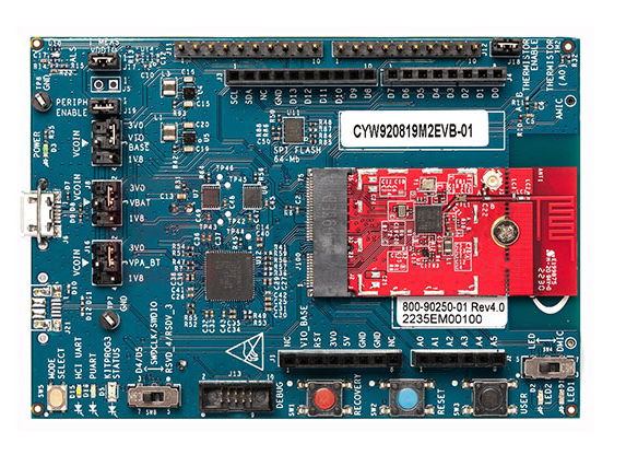
Figure 2 shows CYW920819M2EVB-01 evaluation board with the following features:
1. CYW20819 carrier module with onboard antenna
2. Expansion headers compatible with Arduino shields
3. Support for 1.8 V, 3.0 V, and coin-cell operation of the CYW20819M2EVB-01 device
4. Recovery button (Red), Reset button (Blue), and User button (Black)
5. Onboard micro-USB connector (J6) for programming and debug purposes
The USB micro-B connector (J6) supports UART connections and provides +5 V power to the board. See
Jumpers and Buttons and switches for complete information on DIP switches and jumper settings.
Do the following before connecting the board and verifying the driver installation:
1. Verify that all the jumpers are in the default configuration as shown in Table 4 to Table 9, so that Peripheral
UART is selected and can display embedded application trace messages. Figure 2 shows the default jumper
locations.
2. Connect the USB connector (J6) of the evaluation board to the development PC with the provided USB
cable. The USB UART driver should load automatically. If the evaluation board is not detected as a USB
device, reinstall the USB UART driver in ModusToolbox™ installation directory.
For Windows and macOS: \tools_2.4\driver_media\dpinst.
For Linux: \tools_2.4\driver_media\install_driver\dpinst.
Figure 2
User Guide
CYW920819M2EVB-01 evaluation board
7 of 35
002-36452 Rev. **
2022-10-07
�CYW920819M2EVB-01 evaluation kit user guide
Introduction
Figure 3 highlights the LEDs provided on CYW920819M2EVB-01:
• D3 (Green) indicates that VDD3P0 (3.0 V) power is ON
• D15 (White) indicates HCI UART activity
• D16 (Purple) indicates peripheral UART activity
• D5 (Yellow) indicates KitProg3 status
• D1 (Yellow) and D2 (Red) are generic user LEDs controlled by GPIOs. A label on the back of the kit provides
the pin mapping.
Figure 3
CYW920819M2EVB-01 evaluation board LEDs
1.3
ModusToolbox™
ModusToolbox™ is a free software development ecosystem that includes the Eclipse IDE for ModusToolbox™,
Bluetooth® SDK, and the PSoC™ 6 SDK to develop applications for Infineon IoT products. Eclipse IDE for
ModusToolbox™ is a multi-platform, integrated development environment (IDE) used to create new
applications, update application code, change middleware settings, and program/debug applications.
Using ModusToolbox™, you can enable and configure device resources and middleware libraries, write C source
code, and program and debug the device. The IDE provides hooks for launching various tools provided by the
SDK, called Bluetooth® SDK (BT SDK).
The BT SDK provides the central core of the ModusToolbox™ software for creating Bluetooth® applications. It
contains configuration tools, drivers, libraries, middleware, make files, as well as various utilities, and scripts.
You may use these tools in any development environment you prefer.
For detailed information on ModusToolbox™ installation and usage, see the ModusToolbox™ user guide.
User Guide
8 of 35
002-36452 Rev. **
2022-10-07
�CYW920819M2EVB-01 evaluation kit user guide
Introduction
1.3.1
ModusToolbox™ code examples
ModusToolbox™ includes many code examples. Many of these code examples are compatible with this kit. You
can either browse the collection of starter applications during application set up through File > New >
ModusToolbox™ Application or browse the collection of code examples on Infineon’ GitHub repository. See
Figure 4 and Figure 5 for details.
Figure 4
Code examples in ModusToolbox™
Figure 5
Searching for online code examples in ModusToolbox™
User Guide
9 of 35
002-36452 Rev. **
2022-10-07
�CYW920819M2EVB-01 evaluation kit user guide
Introduction
1.3.2
Related code examples
You can access the kit code examples from the GitHub repository. The CYW920819M2EVB-01 evaluation board
is pre-programmed with the Find Me Profile (CE226123 – BLE Find Me with CYW20819) code example out-of-thebox.
This code example is available in ModusToolbox™ as shown in Figure 4. For the most recent version of the code
example, check the GitHub repository. You can find the CE226123 code example in
github.com/Infineon/mtb-example-btsdk-ble-findme.
For more details on the functionality, design and implementation of the code example, see the code example
document present in the same folder as that of the code example. To import the most recent version of the
GitHub code examples into ModusToolbox™, see the ModusToolbox™ user guide document (Help >
ModusToolbox™ Documentation > User guide).
1.3.3
ModusToolbox™ help
Launch ModusToolbox™ and navigate to the following items:
• Quick Start Guide: Choose Help > Eclipse IDE for ModusToolbox™ Documentation > Quick Start Guide.
This guide gives you the basics for using ModusToolbox™.
• ModusToolbox™ General Documentation: Choose Help > ModusToolbox™ General Documentation >
ModusToolbox™ Documentation Index. This page provides link to various ModusToolbox™ documents.
• ModusToolbox™ User Guide: Choose Help > Eclipse IDE for ModusToolbox™ Documentation > User
Guide. This is a comprehensive guide for creating, building, and programming ModusToolbox™
applications.
1.4
Getting started
This user guide will help you find details of the CYW920819M2EVB-01 Evaluation Kit:
• The Kit operation chapter describes the operation of the kit and how to use its various features.
• The Hardware chapter describes the design details of the CYW920819M2EVB-01 hardware blocks.
1.5
IoT resources and technical support
Infineon provides a wealth of product documentation at https://www.infineon.com/products/wirelessconnectivity to help you to select the right IoT device for your design. Also, a professional community at
community.infineon.com supplies developers the latest software and tools to solve common evaluation and
integration problems while interacting directly with both Infineon engineers and experienced peers.
User Guide
10 of 35
002-36452 Rev. **
2022-10-07
�CYW920819M2EVB-01 evaluation kit user guide
Kit operation
2
Kit operation
This section provides detailed instructions to set up the Infineon CYW920819M2EVB-01 evaluation board to use
with Infineon ModusToolbox™ for Bluetooth® Classic (aka BR - Basic Rate and EDR – Enhanced Data Rate) and
Low Energy (LE) applications.
This chapter introduces you to CYW920819M2EVB-01 and the features that will be used as part of the kit
operation. This chapter also discusses features such as the Bluetooth® connectivity and
programming/debugging as well as the USB-UART bridge device that can be used to communicate with the
CYW20819-A1 device on this EVB.
2.1
Theory of operation
CYW920819M2EVB-01 is built around the CYW20819 device. Figure 6 shows the block diagram of the CYW20819A1 device. See the device datasheet for details on device features.
Figure 6
User Guide
Block diagram of CYW20819
11 of 35
002-36452 Rev. **
2022-10-07
�CYW920819M2EVB-01 evaluation kit user guide
Kit operation
Figure 7 illustrates the block diagram of CYW920819M2EVB-01. This board contains a CYW20819 Bluetooth®
SoC and a USB-Serial interface/programmer. The kit features Arduino form-factor-compatible headers, which
enable Arduino shields to be plugged in, extending the EVB’s capabilities. It also features one user switch, one
reset switch, one recovery switch, two user LEDs, a thermistor, an ambient light sensor, and multiple power
supply options.
Infineon Device
Electric Connection
Analog MIC
Digital MIC
M.2 Bluetooth®/
BLuetooth® LE
Radio Card
Ambient
Light Sensor
No Load
Thermistor
Coin
Cell
Voltage Detector
3.0 V
Reg
USB
Power
32.768-kHz XTAL
M.2 I/O
Interface
Infineon
Bluetooth®/
Bluetooth® LE chip
Buttons
1. Recovery
2. Reset
3. User
1.8 V
Reg
24-MHz
XTAL
Band Pass
Filter
Carrier VBAT, VDDIO and
VDDUSB Monitoring
U.FL
Connector
User LED
Antenna
BT_UART
PUART
PSoC
AIROC Headers
Arduino Headers
(VDDIO/VDD3P0)
External Headers
Figure 7
LP
10-pin
Debugger
(VDDIO)
USB Micro - B
Block diagram of CYW920819M2EVB-01
Figure 8 and Figure 9 show the markup of the CYW920819M2EVB-01 evaluation board. See the list below for a
description of the numbered items.
User Guide
12 of 35
002-36452 Rev. **
2022-10-07
�CYW920819M2EVB-01 evaluation kit user guide
Kit operation
Figure 8
CYW920819M2EVB-01 evaluation board (Top view)
Figure 9
CYW920819M2EVB-01 evaluation board (Bottom view)
1. Peripheral enable (J19): The jumper allows the user to connect and disconnect the VDDIO supply to on-
board peripheral devices like motion sensor, thermistor, analog mic, and real-time clock by disabling VDDP.
2. VIO_BASE select jumper (J7): This jumper is used to select the VIO_BASE power source. Possible selections
are 3.0 V, 1.8 V, or VCOIN, which is the coin-cell power supply on the bottom side of the board.
3. Power indicator LED (D3): This LED is used to indicate the status of power supplied to board.
4. VBAT select jumper (J8): This jumper is used to select the VBAT (core power supply) power source. The
possible selections are 3.0 V, 1.8 V, or VCOIN which is the coin-cell power supply on the bottom side of the
board.
User Guide
13 of 35
002-36452 Rev. **
2022-10-07
�CYW920819M2EVB-01 evaluation kit user guide
Kit operation
5. USB connector (J6): J6 is a micro-B USB female connector for connecting the kit to PC using the provided
USB cable. It is used for programming and USB-UART communication.
6. VPA_BT select jumper (J16): This jumper is used to select the VPA_BT (power amplifier supply) power
source. This select header applies to evaluation boards that has an internal power amplifier and it is not
connected to CYW20819 in CYW920819M2EVB-01 evaluation board.
7. KitProg3 (PSoC™ 5LP) programmer and debugger (CY8C5868LTI-LP039, U12): The PSoC™ 5LP
(CY8C5868LTI-LP039) serving as KitProg3, is a multi-functional system, which includes a Serial Wire Debug
(SWD) programmer, debugger, USB-I2C bridge and USB-UART bridge. For more details, see the KitProg3
user guide.
8. KitProg3 programming mode selection button (SW5): This switch can be used to switch between various
modes of operation of KitProg3 (CMSIS-DAP BULK, CMSIS-DAP HID or DAPLink modes). This switch is not
used for CYW920819M2EVB-01 because the board supports only one mode.
9. HCI-UART indication LED (D15): This White LED indicates the status of HCI-UART.
10. PUART indication LED (D16): This Purple LED indicates the status of PUART.
11. KitProg3 status indication LED (D5): This Yellow LED indicates the status of KitProg3.This is not useful for
CYW920819M2EVB-01 because the board supports only one mode.
12. SWD/GPIO switch (SW8): This switch allows you to route the functionality of GPIO/SWD lines to either J4
Arduino-compatible header or the J13 debug header.
13. Debug header (J13): J13 is a 10-pin interface header that can be used to connect an external debugger via
SWD.
Note: J13 should only be used to connect a debugger. If something else is connected to J13 to
communicate with KitProg3, a voltage mismatch can occur.
14. Recovery button (SW1): This button is used to put the device in recovery mode. To put the device in
recovery mode, press and hold the recovery button, press and release the reset button, and then release the
recovery button. You may need to put the device in recovery mode when the application download fails.
15. Arduino-compatible header (J1): The Arduino-compatible I/O header brings out pins from CYW20819 to
interface with Arduino shields.
16. Reset button (SW2): This button can be used to reset the device.
17. Arduino-compatible header (J2): The Arduino-compatible I/O header brings out pins from CYW20819 to
interface with Arduino shields.
18. User button (SW3): This button can be used to provide an input to the CYW20819 device. Note that the
button connects the CYW20819 pin to ground when pressed; therefore, the CYW20819 pin must be
configured as a digital input with resistive pull-up for detecting the button press.
19. User LEDs (D1 and D2): These onboard LEDs can be controlled by the CYW20819 device. The LEDs are active
LOW; therefore, these pins must be driven to ground to turn ON the LEDs.
20. LED enable switch (SW4): This switch is used to connect/disconnect the user-controlled LEDs from the
CYW20819 device.
21. Carrier module (U1): The carrier module has the CYW20819 SoC on it. A Bluetooth® antenna is etched on
the carrier module PCB. The carrier module is interface with the baseboard through M.2 interface.
22. CYW20819 (U1. U1): The Bluetooth® (BR/EDR- Basic Rate and Enhanced Data Rate) and Bluetooth® Low
Energy 5 qualified system-on-chip from Infineon is the heart of this evaluation kit.
23. PCB antenna (A1): The PCB antenna is the EM wave radiating part of the evaluation board, which is fed
from the BT_RFIO pad of CYW20819 followed by a band-pass filter and an antenna matching circuit.
24. External antenna connector (U1.J3): The external antenna connector is an RF connector fed from the
BT_RFIO pad of the CYW20819 device followed by a band pass filter. See Hardware design guidelines on
the product page for more details.
User Guide
14 of 35
002-36452 Rev. **
2022-10-07
�CYW920819M2EVB-01 evaluation kit user guide
Kit operation
25. Thermistor (TH2): The on-board thermistor is an NTC analog thermistor that can be used to measure
temperature.
26. Thermistor enable jumper (J18): This jumper can be used to connect or disconnect the onboard
thermistor from the CYW20819 device.
27. Arduino-compatible header (J4): The Arduino-compatible I/O header brings out pins from CYW20819 to
interface with Arduino shields.
28. WICED header (J12): This header brings out some pins of the CYW20819 device that are not connected to
the Arduino compatible headers. These pins can be used for testing or for custom applications.
29. Arduino-compatible header (J3): The Arduino-compatible I/O header brings out pins from CYW20819 to
interface with Arduino shields.
30. WICED header (J11): This header brings out some pins of the CYW20819 device that are not connected to
the Arduino compatible headers. These pins can be used for testing or for custom applications.
31. 64-Mb serial flash (U11): This is the 64-Mbit SPI flash used for application purpose.
32. PUART voltage level translator (U8): This voltage level translator IC allows the interoperability of devices
(CYW20819 device and USB/Serial IC) with different high – level and low – level voltages for input and output
operations.
33. HCI-UART voltage level translator (U7): This voltage level translator IC allows interoperability of devices
(CYW20819 device and USB/Serial IC) with different high-level and low-level voltages for input and output
operations.
34. VDDIO current measurement jumper (J17): This jumper is used to power the carrier module. To measure
the current consumed by the carrier module, remove this jumper and connect an ammeter to the two pins.
35. Ambient light sensor (U14): This is an I2C-based ambient light sensor.
36. Analog mic (MIC1): It is not supported by CYW20819.
37. Digital mic (U13): The digital microphone ASIC contains an extremely low – noise preamplifier and a highperformance sigma-delta ADC.
38. Debug/programming mode select switch (SW15): This switch allows you to route the functionality of
KitProg3/GPIO lines to either the PSoC™ 5LP based KitProg3 or J4 Arduino-compatible header.
39. Coin cell holder (BT1): This is a coin cell battery holder located on the bottom side of the development kit.
If the evaluation board needs to use the power supplied from the coin cell, then the VDDIO, VBATT and
VPA_BT select headers must be set to VCOIN.
40. P-UART flow control switch (SW17): This switch allows you to enable and disable the PUART flow control
functionality.
2.2
Jumpers
Table 4 to Table 9 list the jumper settings on the CYW920819M2EVB-01 board.
Table 4
Jumper J7 pin configurations
Jumper J7
(VIO_BASE
selection)
Default state
Connection on
CYW20819
Description
2 and 3
Shorted
VDDO1, VDDO2
Short these pins to supply 3.0 V to VIO_BASE of the
CYW20819 device, as well as all peripherals and
sensors.
3 and 4
Open
User Guide
Short these pins to supply 1.8 V to VIO_BASE of the
CYW20819 device, as well as all peripherals and
sensors.
15 of 35
002-36452 Rev. **
2022-10-07
�CYW920819M2EVB-01 evaluation kit user guide
Kit operation
Jumper J7
(VIO_BASE
selection)
Default state
1 and 3
Open
Table 5
Connection on
CYW20819
Description
Short these pins to supply VIO_BASE of the
CYW20819 device, as well as all peripherals and
sensors from the coin cell supply (VCOIN).
Jumper J8 pin configurations
Jumper J8 (VBAT
selection)
Default state
Connection on
CYW20819
Description
2 and 3
Shorted
SR_PVDD,
PMU_AVDD
Short these pins to supply 3.0 V to VBAT of the
CYW20819 device. Also, use this jumper to measure
the current consumption of VBATT when using 3.0V supply.
3 and 4
Open
Short these pins to supply 1.8 V to VBATT of the
CYW20819 device. Also, use this jumper to measure
the current consumption of VBATT when using 1.8V supply.
1 and 3
Open
Short these pins to use the coin cell supply VBATT
of the CYW20819 device. Also, use this jumper to
measure the current consumption of VBATT when
using the coin cell supply (VCOIN).
Table 6
Jumper J18 pin configuration
Jumper J18
(Thermistor
connect/
disconnect)
Default state
Connection on
CYW20819
Description
1 and 2
Shorted
P8
Short this jumper to connect the on-board
thermistor to CYW20819.
Table 7
Jumper J17 pin configuration
Jumper J17
(VDDIO current
measurement)
Default state
Connection on
CYW20819
Description
1 and 2
Shorted
VDDIO1, VDDIO2
Short this jumper to supply power to the I/O
domain (VDDIO) of CYW20819. Also, use this jumper
to measure the current consumption of the I/O
domain.
Table 8
Jumper J19 pin configuration
Jumper J19
(Peripheral
enable)
Default state
Connection on
CYW20819
Description
1 and 2
Shorted
NA
Allows power to on-board peripherals such as
ambient light sensor.
User Guide
16 of 35
002-36452 Rev. **
2022-10-07
�CYW920819M2EVB-01 evaluation kit user guide
Kit operation
Table 9
Jumper J16 pin configurations
Jumper J16
(VPA_BT current
measurement)
Default state
Connection on
CYW20819 device
2 and 3
Shorted
NC_0
(PALDO_VDDIN)
3 and 4
Open
This select header applies to evaluation boards
that has an internal power amplifier and it is not
connected to CYW20819 in the CYW920819M2EVB01 evaluation board.
1 and 3
Open
This select header applies to evaluation boards
that has an internal power amplifier and it is not
connected to CYW20819 in the CYW920819M2EVB01 evaluation board.
This select header applies to evaluation boards
that has an internal power amplifier and it is not
connected to CYW20819 in the CYW920819M2EVB01 evaluation board.
Note:
VDDIO must be greater or equal to VBATT. CYW20819 uses an on-chip low-voltage detector to shut
down the chip when supply voltage (VBATT) drops below the operating range. The shutdown
voltage (VSHUT) lies between a minimum of 1.5 V and a maximum of 1.7 V. See the datasheet for
more details.
2.3
Buttons and switches
Table 10
Button functionality
Buttons
Pressed state
Connection on
CYW20819
Description
SW1
GND
RECOVER
Recovery button* (Red)
SW2
GND
RST_N
Active LOW Reset button (Blue)
SW3
GND
P0
User application button (Black)
Note:
*See the Recovery button (SW1): under Theory of operation.
The switch SW4 enables or disables the two onboard user LEDs. By default, both LED1 and LED2 are enabled.
Table 11
SW4 slide switches configuration
SW4
Default state
Connection on
CYW20819
Description
POS 1
ON
NC
Enables LED1
ON
NC
Enables LED2
OFF
NC
Enables DMIC_CLK
OFF
NC
Enables DMIC_DATA
POS 2
SW8 is a slide switch. Pos 1 allows RSVD_4 and RSVD_5 to be used for SWD functionality for the debugger
interface. Pos 2 allows P2 and P3 to be used for SWD functionality for the debugger interface and when using P2
and P3 as GPIOs, keep SW8 in the Pos2 position.
User Guide
17 of 35
002-36452 Rev. **
2022-10-07
�CYW920819M2EVB-01 evaluation kit user guide
Kit operation
Table 12
SW8 slide switches configuration
Slide SW8
Default state
Connection on
CYW20819
Description
POS 1
OFF
RSVD_4
Connects RSVD_4 to the Arduino-compatible header
pin RSVD_4 if the slide switch is in the OFF state.
Connects RSVD_4 to the debug header if the slide
switch is in the ON state.
OFF
RSVD_5
Connects RSVD_5 to the Arduino-compatible header
RSVD_5 if the slide switch is in the OFF state.
Connects RSVD_5 to the debug header if the switch
is in the ON state.
ON
P2
Connects P2 to the Arduino-compatible header pin
ARD_D4_SWDCLK if the slide switch is in the OFF
state. Connects P2 to the debug header if the slide
switch is in the ON state.
ON
P3
Connects P3 to the Arduino-compatible header pin
ARD_D45SWDIO if the slide switch is in the OFF
state. Connects P3 to the debug header if the slide
switch is in the ON state.
POS 2
2.4
Arduino-compatible headers
J3, J4, J11, and J12 are the Arduino-compatible headers.
Table 13
Header J3 pin configuration
Header J3
Arduino pin
Connection on
CYW20819
WICED Enum
name
Description
1
SCL
P26
WICED_P26
I2C SCL
2
SDA
P27
WICED_P27
I2C SDA
3
AREF
NC
-
NC
4
GND
GND
-
Ground
5
D13
P9
WICED_P09
GPIO
6
D12
P17
WICED_P17
GPIO
7
D11
P6
WICED_P06
GPIO
8
D10
P15
WICED_P15
GPIO
9
D9
NC
-
NC
10
D8
P14
WICED_P14
GPIO
Table 14
Header J4 pin configuration
Header J4
Arduino pin
Connection on
CYW20819
WICED Enum
name
Description
1
D7
P5
WICED_P05
GPIO
2
D6
P4
WICED_P04
GPIO
3
D5
P3
WICED_P03
GPIO
4
D4
P2
WICED_P02
GPIO
5
D3
P1
WICED_P01
GPIO
6
D2
P0
WICED_P00
User button
User Guide
18 of 35
002-36452 Rev. **
2022-10-07
�CYW920819M2EVB-01 evaluation kit user guide
Kit operation
Header J4
Arduino pin
Connection on
CYW20819
WICED Enum
name
Description
7
D1
P32
WICED_P32
PUART RX
8
D0
P37
WICED_P37
PUART TX
Table 15
Header J1 pin configuration
Header J1
Arduino pin
Connection on CYW20819
Description
1
NC
NC
NC
2
VIO_BASE
VDDIO
I/O reference pin used by shields to determine
the I/O voltage. Connected to VDDIO on this
board. Therefore, IOREF follows 1.8 V or 3.0 V,
or VCOIN of VDDIO.
3
RST
ARD_RST/P1
Arduino Reset (R72 install position A) (See
Device reset) / P1 (R72 install position B).
4
3V0
VDD3P0
3.0-V supply output to the Arduino Shield.
5
5V
VDD5V
5-V supply output to the Arduino Shield.
6
GND
GND
Ground
7
GND
GND
Ground
8
NC
NC
NC
Table 16
Header J2 pin configuration
Header J2
Arduino pin
Connection on
CYW20819
WICED Enum
name
Description
1
A0
P8
WICED_P08
GPIO/Thermistor
2
A1
NC
-
-
3
A2
P10
WICED_P10
GPIO/PUART CTS
4
A3
NC
-
-
5
A4
P12
WICED_P12
GPIO
6
A5
P13
WICED_P13
GPIO
Note:
When accessing Arduino pins, remove the jumpers that may interfere with the Arduino pins such as
PUART jumpers and thermistor jumper.
2.5
Other headers
J11 and J12 are test headers which bring out certain pins of CYW20819 for testing.
Table 17
Header J11 pin description
Header J11
Connection to
header pin
Connection on
CYW20819
WICED Enum
name
Description
1
BT_UART_CTS_L
BT_UART_CTS
WICED_P27
BT_UART_CTS
2
LED1_L
P29
WICED_P26
LED1 connection.
3
LED2_L
P28
–
LED2 connection.
4
RSVD_10
P9
–
SF_SCLK
5
RSVD_11
DEV_WAKE
–
Signal to wake up the device
User Guide
19 of 35
002-36452 Rev. **
2022-10-07
�CYW920819M2EVB-01 evaluation kit user guide
Kit operation
Header J11
Connection to
header pin
Connection on
CYW20819
WICED Enum
name
Description
6
RSVD_12
HOST_WAKE
–
Signal to wake up the host
7
COEX1
NC
–
No connect.
8
COEX2
NC
–
No connect.
9
COEX3
NC
–
No connect.
10
GND
GND
–
Ground.
Table 18
Header J12 pin description
Header J12
Connection to header pin
Connection on CYW20819
Description
1
RSVD_1_USER_BTN
P0
SW3 user button connection.
2
RSVD_2
NC
No connect.
3
RSVD_3
NC
No connect.
4
RSVD_4
NC
No connect.
5
RSVD_5
NC
No connect.
6
RSVD_6
P6
SF_MOSI.
7
RSVD_7
P17
SF_MISO.
8
RSVD_8
NC
Ambient light sensor INT.
9
RSVD_9
P11 (WICED_P11)
SPI (Slave select) external flash
memory.
10
VIO_BASE
NC
J13 is a 10-pin debugger header to debug CYW920819M2EVB-01 using SWD.
Table 19
Header J13 pin description
Header J13
Connection to
header pin
Connection on
CYW20819
1
VDDIO
VDDIO
2
D5/SWDIO
P3
3
GND
GND
4
D4/SWDCK
P2
WICED_P02
Serial wire debug clock.
SW9 switch 1 must be in the OFF
position for this connection to be
made.
5
GND
GND
–
Ground.
6
NC
NC
–
No connect.
7
GND
GND
–
Ground.
8
NC
NC
–
No connect.
9
GND
GND
–
Ground.
10
SWD_RST
BT_RST_N
–
CYW20819 device reset.
Note:
User Guide
WICED Enum
name
Description
VDDIO reference.
WICED_P03
Serial wire debug input output. SW9
switch 2 must be in the OFF position
for this connection to be made.
Ground.
J13 should be used only to connect a debugger. If not, a voltage mismatch can occur.
20 of 35
002-36452 Rev. **
2022-10-07
�CYW920819M2EVB-01 evaluation kit user guide
Kit operation
2.6
USB serial interface chip
A CY8C5868LTI-LP039 PSoC™ 5 LP chip is used for onboard programming and USB-Serial functionality. It
connects to the computer over a USB interface and connects to the CYW20819-A1 device through the HCI UART
and PUART pins.
2.7
Kit power supply
The kit can be powered by one of two power sources: USB or coin-cell battery.
As shown in Figure 7, the USB power is connected to two buck regulators, one regulating the voltage to 1.8 V
and the other to 3.0 V. A coin-cell battery can be directly connected without the need of a regulator. See
Table 4, Table 5, Table 7, and Table 9 to understand the jumper settings for power selection.
2.8
Test points
There are two ground test points for easy connection of probes. The voltage from various power domains can
be measured from their respective headers (J7, J8, and J16).
Table 20
Ground test points available in CYW920819M2EVB-01
Label
Description
TP7, TP8
2.9
Test points for ground
Current measurement
The CYW20819 device has two power domains:
• VIO_BASE to power the always ON GPIO pins
• VBAT to power the core
The total current consumption by the device is the sum of the current consumed by the VIO_BASE and VBAT
power domains.
• To measure the current consumed by the VIO_BASE domain, connect an ammeter across jumper J17.
• To measure the current consumed by the VBAT domain, connect an ammeter across pin 3 and one of pins 1,
2, or 4 (depending on the power source) of jumper J8.
2.10
SWD debugging
ModusToolbox™ supports multiple Arm®-JTAG adapters for debugging Bluetooth® products like CYW20819.
Debugging is possible on CYW920819M2EVB-01 through SWD signals. SWD is a 2-wire interface that uses SWD
input output (SWDIO) and serial wire clock (SWDCK) for debugging the device. These two lines can be brought
out to any of the LHL GPIOs on CYW20819. In CYW920819M2EVB-01, P3 will act as SWDIO and P2 will act as
SWDCK. See Table 19 to enable SWD pins to the debug connector (J13).
After making these hardware configurations, see the Debugger guide (/libraries/bt_sdk/docs/BT-SDK/ WICED-Hardware-Debugging.pdf) for debugging your application using
ModusToolbox™. This guide can also be accessed from Eclipse IDE for ModusToolbox™ under the menu item
Help > ModusToolbox™ General Documentation > ModusToolbox™ Documentation Index > Bluetooth®
Documentation > Hardware Debugging for WICED Devices.
User Guide
21 of 35
002-36452 Rev. **
2022-10-07
�CYW920819M2EVB-01 evaluation kit user guide
Kit operation
2.11 Pin configuration
GPIOs on the CYW20819 device can be multiplexed to various peripherals. For more information on the
peripherals that can be routed to the various GPIOs, see the device datasheet.
For this board, the ModusToolbox™ software initializes GPIOs to the platform default configuration. For
example, P26 and P27 are configured as I2C SCL and I2C SDA, respectively.
User Guide
22 of 35
002-36452 Rev. **
2022-10-07
�CYW920819M2EVB-01 evaluation kit user guide
Hardware
3
Hardware
This chapter describes the CYW920819M2EVB-01 hardware and its different blocks such as reset control,
Arduino-compatible headers, and module connectors.
The schematics for the baseboard and carrier module can be found on the CYW920819M2EVB-01 kit page.
3.1
Carrier module
The baseboard of the CYW920819M2EVB-01 board is designed to be modular so that various carrier modules
can be used with the same baseboard. In this kit, the CYW920819M2IPA1 carrier M.2 radio card module, which
employs the CYW20819 device, is connected to the baseboard through M.2 Interface. The carrier module
interface is a generic interface that can be used across may devices. See CYW20819 device I/O mapping for a
detailed interface description. The Bluetooth® antenna is etched on the carrier module PCB. UART signals and
GPIOs are brought out to module pins to interface with the baseboard.
3.1.1
CYW20819
The CYW920819M2EVB-01 board employs the CYW20819A1KFBG device which is a 62-BGA package. This board
uses all 22 LHL GPIOs provided by the 62-BGA package.
3.1.2
Antenna
A PCB antenna is etched on the carrier module. This antenna is matched to 50 Ω when the CYW920819M2EVB01 board is placed on a table. Table 21 lists the S11 measurement. See AN91445 – Antenna design and RF
layout guidelines for additional information.
Table 21
Antenna S11 measurement
2402 MHz
2441 MHz
2480 MHz
-13.2 dB
-14.6 dB
-12.6 dB
3.1.3
Crystal
The CYW20819 carrier module has two crystals on-board. A 24-MHz crystal (XTAL) is the main crystal. This XTAL
must have an accuracy of +/-20 ppm as defined by the Bluetooth® specification. A 32.768-kHz crystal provides
accurate timing during low-power operation. See the CYW20819 datasheet for crystal requirements.
3.2
Baseboard
CYW9BTM2BASE2 is a baseboard on which the CYW20819 carrier module is connected to.
User Guide
23 of 35
002-36452 Rev. **
2022-10-07
�CYW920819M2EVB-01 evaluation kit user guide
Hardware
3.3
Serial communication between CYW20819 and PSoC™ 5 KitProg3
The onboard CY8C5868LTI-LP039 PSoC™ 5LP device is a true programmable embedded system-on-chip
responsible for two channel USB-Serial conversion on this baseboard. The USB-serial pins of the PSoC™ 5LP
device are hard-wired to the HCI UART and PUART pins of the CYW20819 device. Because PUART RTS is not
routed to the USB-Serial device, any of the available LHL GPIOs can be assigned as PUART RTS using the Device
Configurator utility and connected using a jumper wire to the assigned Arduino header to use the flow control
mechanism provided by the PUART.
Note:
For applications involving low-power modes, the CYW920819M2EVB-01 evaluation board needs to
be reset after plugging it into the computer. This is due to the behavior of the serial
communication chip where it asserts the CTS pin for some time on power-up, which prevents the
CYW920819M2EVB-01 evaluation board from entering the low-power mode.
3.4
Power
The power supply system on this board is versatile, allowing the input supply to come from the following
sources:
• 1.8 V or 3.0 V from the on-board USB connector.
• 3 V from a coin cell battery.
Figure 10 shows the power architecture of the CYW920819M2EVB-01 evaluation board.
PSoC 5LP
Arduino headers
VDDUSB
USB
Micro - B
3.0V Reg
VDDP
Peripherals
• Analog mic
• Digital mic
• Serial flash
• Ambient light sensor
• Thermistor
1.8V Reg
VDDIO/
VBAT/
VPA_BT
Coin cell
Figure 10
User Guide
M.2 card
Power Hi
24 of 35
002-36452 Rev. **
2022-10-07
�CYW920819M2EVB-01 evaluation kit user guide
Hardware
Power supply options can be selected via jumper settings on J7, J8, and J16. See Table 4, Table 5, and
Table 9 for the different jumper settings for these jumpers. Resistors R25 and R21 are pull-up resistors for the
I2C lines to the ambient light sensor i.e., SCL and SDA. Note that J19 (PERIPH ENABLE) should be shorted for any
I2C devices to be connected because the pull-up voltages for SCL and SDA are supplied from VDDP. The VPA_BT
selection jumper (J16) applies to evaluation boards that has an internal power amplifier connected to the
Bluetooth® chip and does not apply to CYW920819M2EVB-01 evaluation kit.
Figure 11
5-V power supply from USB
Figure 12
3.0-V regulator circuit
User Guide
25 of 35
002-36452 Rev. **
2022-10-07
�CYW920819M2EVB-01 evaluation kit user guide
Hardware
Figure 13
1.8-V regulator circuit
Figure 14
Jumper J7 for VDDIO selection
Figure 15
Jumper J8 for VBAT selection
User Guide
26 of 35
002-36452 Rev. **
2022-10-07
�CYW920819M2EVB-01 evaluation kit user guide
Hardware
Figure 16
Jumper J16 for VPA_BT selection (NC)
3.5
Device reset
The reset circuit on the board consists of a Reset button (SW2) connected to ground and a voltage detector IC.
The RST_N pin on CYW20819 should be released after 50 ms or more after the VDDIO supply voltage has
stabilized. The voltage-detector IC is used to provide this delay.
Figure 17
Reset button circuit
Figure 18
Voltage detector circuit in the carrier module
In the default configuration of R40 shown below (position A-C), the reset button is routed to the Arduinocompatible header reset pin in addition to the device, so both the device and shields can be reset by pressing
SW2. Alternatively, in this case, the device can be reset by driving the Arduino-compatible header reset pin LOW
allowing for an external reset source.
When R40 is in position (B-C), the device pin P1 will be routed to the ARD_RST header if R13 on device module is
installed (default is DNI), so the reset button will not trigger the Arduino-compatible header reset pin, but
device pin P1 can be used to monitor or drive the Arduino-compatible header reset pin.
User Guide
27 of 35
002-36452 Rev. **
2022-10-07
�CYW920819M2EVB-01 evaluation kit user guide
Hardware
The reset button (SW2) always connects to the BT_RST input on the device so that the device can be reset by
pushing the button in either configuration.
Figure 19
Reset to Arduino-compatible header
Figure 20
P1 to ARD_RST_N R13 resistor
3.6
Thermistor
The thermistor circuit is a simple voltage divider circuit consisting of an NTC thermistor that is 100 kΩ at 25°C
and a fixed 100-kΩ resistor. The divided voltage is fed in to A0 and the voltage level determines the ambient
temperature. The part number of the thermistor used on this kit is NCU15WF104F60RC.
Figure 21
User Guide
Thermistor circuit
28 of 35
002-36452 Rev. **
2022-10-07
�CYW920819M2EVB-01 evaluation kit user guide
Hardware
3.7
External serial flash
CYW920819M2EVB-01 has a GigaDevice GD25WQ64ENIG is the 64-Mbit serial flash on the baseboard, which can
be useful when the user application requires more memory. The BT SDK is compatible with most JEDEC CFIcompliant SPI flash ICs. The SPI driver should configure the respective pins in the user application in order to
use the onboard serial flash.
Figure 22
External serial flash
3.8
Ambient light sensor
CYW920819M2EVB-01 has an onboard light-to-digital sensor (Texas Instruments OPT3002DNPT). It has a wide
spectral bandwidth, ranging from 300 nm to 1000 nm. Measurements can be made from 1.2 nW/cm2 up to
10 mW/cm2. The CYW20819 device communicates with this sensor over I2C. The I2C address is 0x4D for high 0x4C
for low. See the OPT3002DNPT datasheet for more details.
Figure 23
User Guide
Ambient light sensor circuit
29 of 35
002-36452 Rev. **
2022-10-07
�CYW920819M2EVB-01 evaluation kit user guide
Hardware
3.9
LEDs
There are two onboard user LEDs on the kit. LED1 is controlled by P29. LED2 is controlled by P28. You can
enable or disable the LEDs using slide switch SW4. See Table 11 for slide switch configuration. TLMY1000-GS08
(Yellow) from Vishay Intertechnology requires a typical voltage of at least 1.8 V (can be as high as 2.6 V) to
operate. LTST-C190CKT (Red) from Lite-On Technology Corporation requires a typical voltage of at least 1.8 V
(can be as high as 2.4 V) to operate.
Note:
LEDs are initialized by default on boot-up. See the following file for the LED enumeration in the
SDK. This file will also be accessible from the Workspace Explorer in Eclipse IDE for ModusToolbox™
after you create an application for this kit.
\libraries\bt_sdk-\components\BT-SDK\208XX-A1_Bluetooth\platforms\CYW920819M2EVB_01\
wiced_platform.h
Figure 24
LED circuit
3.10
Push buttons
CYW920819M2EVB-01 has a reset button, recovery button, and a user button. See the Device reset section for
details on the reset button. See the Buttons and switches section for details on using the recovery button
during kit programming. One user button (SW3) is connected to pin P0 of the CYW20819 device.
Note:
The user button is initialized by default on bootup. See the following file for the button
enumeration in the SDK. This file will also be accessible from the Workspace Explorer in Eclipse IDE
for ModusToolbox™ after you create an application for this kit.
\libraries\bt_sdk-\components\BT-SDK\208XX-A1_Bluetooth\platforms\
CYW920819M2EVB_01\wiced_platform.h
User Guide
30 of 35
002-36452 Rev. **
2022-10-07
�CYW920819M2EVB-01 evaluation kit user guide
CYW20819 device I/O mapping
4
CYW20819 device I/O mapping
Table 22 maps the CYW20819 device I/Os to headers and sensors on the baseboard. It also lists the carrier
module interface definition.
Note:
**: MIC1 is not populated in CYW920819M2EVB-01.
Table 22
Carrier module interface and pin connections
Carrier
module
pin
Carrier module pin
name
CYW20819
pin
Baseboard
connection 1
Baseboard
connection 2
Baseboard
connection 3
WICED Enum
name
1
GND
GND
Ground
–
–
–
2
VPA_BT
VPA_BASE
VPA_BT
J16.3
–
–
3
BT_USB_DP
NC
J21.3
–
–
4
VPA_BT
VPA_BASE
J16.3
–
–
5
BT_USB_DN
NC
J21.2
–
–
6
LED_1L
P29
SW4.2
J11.2
–
WICED_P29
7
GND
GND
Ground
–
–
–
8
ARD_A4
P12
J2.5
–
–
WICED_P12
9
ARD_D13
P9
J3.5
–
–
WICED_P09
10
ARD_A5
P13
J2.6
–
–
WICED_P13
11
ARD_D8
P14
J3.10
–
–
WICED_P14
12
ARD_D6
P4
J4.2
–
–
WICED_P04
13
ARD_D12
P17
J3.6
–
–
WICED_P17
14
ARD_D7
P5
J4.2
–
–
WICED_P05
15
ARD_D11
P6
J3.7
–
MIC1**
WICED_P06
16
LED2_L
P28
SW4.6
J11.3
17
ARD_A0_THERMISTO
R
P8
J2.1
J18.1
–
WICED_P08
18
GND
GND
Ground
–
–
–
19
ARD_A1
NC
J2.2
–
–
–
20
RSVD_12
HOST_
WAKE
J11.6
–
–
–
21
ARD_D10
P15
J3.8
–
–
WICED_P15
22
BT_UART_TX
BT_UART_T
X
U12.21
–
–
–
23
ARD_D2
P0
J4.6
–
–
WICED_P00
32
BT_UART_RX
BT_UART_R
X
U12.20
–
–
–
33
RSVD_10
P9
U11.6
J11.4
–
WICED_P09
34
BT_UART_RTS_L
BT_UART_
RTS
U7.5
–
–
–
35
ARD_D4_SWDCLK
P2
J4.4
SW15.4
SW8.3
WICED_P02
36
BT_UART_CTS_L
BT_UART_
CTS
U7.6
–
–
–
37
ARD_D5_SWDIO
P3
J4.3
SW15.1
SW8.7
WICED_P03
User Guide
VPA_BT
31 of 35
WICED_P28
002-36452 Rev. **
2022-10-07
�CYW920819M2EVB-01 evaluation kit user guide
CYW20819 device I/O mapping
Carrier
module
pin
Carrier module pin
name
CYW20819
pin
Baseboard
connection 1
Baseboard
connection 2
Baseboard
connection 3
WICED Enum
name
38
ARD_D3
P1
J4.5
–
–
WICED_P01
39
GND
GND
Ground
–
–
–
40
ARD_D9
NC
J3.9
–
–
–
41
RSVD_4
NC
SW8.1
J12.4
–
–
42
RSVD_11/VDD2P5
DEV_WAKE
J5.1
J11.5
–
–
43
RSVD_3
NC
SW8.5
J12.3
–
–
44
COEX3
NC
J11.9
–
–
–
45
GND
GND
Ground
–
–
–
46
COEX2
NC
J11.8
–
–
–
47
MIC_P
NC
MIC1.1
–
–
–
48
COEX1
NC
J11.7
–
–
–
49
MIC_N
NC
Ground
–
–
–
50
EXT_LPO
EXT_LPO
NC
–
–
–
51
GND
GND
Ground
–
–
–
52
ARD_RST_N
P1
R40.B
–
–
WICED_01
53
MIC_BIAS
NC
–
–
–
–
J13.10
U12.3
–
54
BT_RST_N
RST_N
SW2.3/4
(RESET_
BTN)
55
MIC_AVDD
NC
VIO_BASE
–
–
–
56
RSVD_9
P11
U11.1
J12.9
–
WICED_P11
57
GND
GND
Ground
–
–
–
58
SDA
P27
J3.2
U10.6
U3.2
WICED_P27
59
RSVD_2
NC
U11.3
J12.2
–
60
SCL
P26
J3.1
U10.4
U3.6
WICED_P26
61
RSVD_1/
USER_BTN
P0
SW3.2/1
(USER_
BTN)
J12.1
–
–
62
RSVD_8
NC
U10.5
J12.8
–
–
63
RECOVERY
BT_UART_
CTS
SW1.3/4
(RECOVERY_
BTN)
–
–
–
64
VDDIO
VDDIO
J17.1
–
–
65
ARD_A3
P29
J2.4
SW17.1
–
WICED_P29
66
RSVD_7
P17
U11.2
J12.7
–
WICED_P17
67
ARD_A2
P10
J2.3
SW17.4
–
WICED_P10
68
RSVD_6
P6
U11.5
J12.6
–
WICED_P06
69
GND
GND
Ground
–
–
–
70
RSVD_5
NC
U11.7
J12.5
–
71
ARD_D1
P32
J4.7
U8.1
–
WICED_P32
72
VBAT
VBAT
VBAT
J8.3
U12.8
–
73
ARD_D0
P37
J4.8
U8.2
–
WICED_P37
User Guide
32 of 35
002-36452 Rev. **
2022-10-07
�CYW920819M2EVB-01 evaluation kit user guide
CYW20819 device I/O mapping
Carrier
module
pin
Carrier module pin
name
CYW20819
pin
Baseboard
connection 1
Baseboard
connection 2
Baseboard
connection 3
WICED Enum
name
74
VBAT
VBAT
VBAT
J8.3
U12.8
–
75
GND
GND
Ground
–
–
–
User Guide
33 of 35
002-36452 Rev. **
2022-10-07
�CYW920819M2EVB-01 evaluation kit user guide
Revision history
Revision history
Date
Version
Description
2022-10-07
**
Initial release
User Guide
34 of 35
002-36452 Rev. **
2022-10-07
�Trademarks
All referenced product or service names and trademarks are the property of their respective owners.
Edition 2022-10-07
Published by
Infineon Technologies AG
81726 Munich, Germany
© 2022 Infineon Technologies AG.
All Rights Reserved.
Do you have a question about this
document?
Go to www.infineon.com/support
Document reference
002-36452 Rev. **
IMPORTANT NOTICE
The information given in this document shall in no
event be regarded as a guarantee of conditions or
characteristics (“Beschaffenheitsgarantie”).
With respect to any examples, hints or any typical
values stated herein and/or any information
regarding the application of the product, Infineon
Technologies hereby disclaims any and all
warranties and liabilities of any kind, including
without limitation warranties of non-infringement of
intellectual property rights of any third party.
In addition, any information given in this document
is subject to customer’s compliance with its
obligations stated in this document and any
applicable legal requirements, norms and standards
concerning customer’s products and any use of the
product of Infineon Technologies in customer’s
applications.
The data contained in this document is exclusively
intended for technically trained staff. It is the
responsibility of customer’s technical departments
to evaluate the suitability of the product for the
intended application and the completeness of the
product information given in this document with
respect to such application.
For further information on the product, technology,
delivery terms and conditions and prices please
contact your nearest Infineon Technologies office
(www.infineon.com).
WARNINGS
Due to technical requirements products may contain
dangerous substances. For information on the types
in question please contact your nearest Infineon
Technologies office.
Except as otherwise explicitly approved by Infineon
Technologies in a written document signed by
authorized
representatives
of
Infineon
Technologies, Infineon Technologies’ products may
not be used in any applications where a failure of the
product or any consequences of the use thereof can
reasonably be expected to result in personal injury.
�