Please note that Cypress is an Infineon Technologies Company.
The document following this cover page is marked as “Cypress” document as this is the
company that originally developed the product. Please note that Infineon will continue
to offer the product to new and existing customers as part of the Infineon product
portfolio.
Continuity of document content
The fact that Infineon offers the following product as part of the Infineon product
portfolio does not lead to any changes to this document. Future revisions will occur
when appropriate, and any changes will be set out on the document history page.
Continuity of ordering part numbers
Infineon continues to support existing part numbers. Please continue to use the
ordering part numbers listed in the datasheet for ordering.
www.infineon.com
�CYW943907AEVAL1F
Evaluation Kit User Guide
Document Number: 002-18703 Rev. *D
Cypress Semiconductor
An Infineon Technologies Company
198 Champion Court
San Jose, CA95134-1709
www.cypress.com, www.infineon.com
�Copyrights
© Cypress Semiconductor Corporation, 2017-2020. This document is the property of Cypress Semiconductor
Corporation and its subsidiaries (“Cypress”). This document, including any software or firmware included or
referenced in this document (“Software”), is owned by Cypress under the intellectual property laws and treaties
of the United States and other countries worldwide. Cypress reserves all rights under such laws and treaties and
does not, except as specifically stated in this paragraph, grant any license under its patents, copyrights,
trademarks, or other intellectual property rights. If the Software is not accompanied by a license agreement and
you do not otherwise have a written agreement with Cypress governing the use of the Software, then Cypress
hereby grants you a personal, non-exclusive, nontransferable license (without the right to sublicense) (1) under
its copyright rights in the Software (a) for Software provided in source code form, to modify and reproduce the
Software solely for use with Cypress hardware products, only internally within your organization, and (b) to
distribute the Software in binary code form externally to end users (either directly or indirectly through resellers
and distributors), solely for use on Cypress hardware product units, and (2) under those claims of Cypress’s
patents that are infringed by the Software (as provided by Cypress, unmodified) to make, use, distribute, and
import the Software solely for use with Cypress hardware products. Any other use, reproduction, modification,
translation, or compilation of the Software is prohibited.
TO THE EXTENT PERMITTED BY APPLICABLE LAW, CYPRESS MAKES NO WARRANTY OF ANY KIND,
EXPRESS OR IMPLIED, WITH REGARD TO THIS DOCUMENT OR ANY SOFTWARE OR ACCOMPANYING
HARDWARE, INCLUDING, BUT NOT LIMITED TO, THE IMPLIED WARRANTIES OF MERCHANTABILITY
AND FITNESS FOR A PARTICULAR PURPOSE. No computing device can be absolutely secure. Therefore,
despite security measures implemented in Cypress hardware or software products, Cypress shall have no liability
arising out of any security breach, such as unauthorized access to or use of a Cypress product. CYPRESS
DOES NOT REPRESENT, WARRANT, OR GUARANTEE THAT CYPRESS PRODUCTS, OR SYSTEMS
CREATED USING CYPRESS PRODUCTS, WILL BE FREE FROM CORRUPTION, ATTACK, VIRUSES,
INTERFERENCE, HACKING, DATA LOSS OR THEFT, OR OTHER SECURITY INTRUSION (collectively,
“Security Breach”). Cypress disclaims any liability relating to any Security Breach, and you shall and hereby do
release Cypress from any claim, damage, or other liability arising from any Security Breach. In addition, the
products described in these materials may contain design defects or errors known as errata which may cause
the product to deviate from published specifications. To the extent permitted by applicable law, Cypress reserves
the right to make changes to this document without further notice. Cypress does not assume any liability arising
out of the application or use of any product or circuit described in this document. Any information provided in this
document, including any sample design information or programming code, is provided only for reference
purposes. It is the responsibility of the user of this document to properly design, program, and test the
functionality and safety of any application made of this information and any resulting product. “High-Risk Device”
means any device or system whose failure could cause personal injury, death, or property damage. Examples
of High-Risk Devices are weapons, nuclear installations, surgical implants, and other medical devices. “Critical
Component” means any component of a High-Risk Device whose failure to perform can be reasonably expected
to cause, directly or indirectly, the failure of the High-Risk Device, or to affect its safety or effectiveness. Cypress
is not liable, in whole or in part, and you shall and hereby do release Cypress from any claim, damage, or other
liability arising from any use of a Cypress product as a Critical Component in a High-Risk Device. You shall
indemnify and hold Cypress, its directors, officers, employees, agents, affiliates, distributors, and assigns
harmless from and against all claims, costs, damages, and expenses, arising out of any claim, including claims
for product liability, personal injury or death, or property damage arising from any use of a Cypress product as a
Critical Component in a High-Risk Device. Cypress products are not intended or authorized for use as a Critical
Component in any High-Risk Device except to the limited extent that (i) Cypress’s published data sheet for the
product explicitly states Cypress has qualified the product for use in a specific High-Risk Device, or (ii) Cypress
has given you advance written authorization to use the product as a Critical Component in the specific High-Risk
Device and you have signed a separate indemnification agreement.
Cypress, the Cypress logo, Spansion, the Spansion logo, and combinations thereof, WICED, PSoC, CapSense,
EZ-USB, F-RAM, and Traveo are trademarks or registered trademarks of Cypress in the United States and other
countries. For a more complete list of Cypress trademarks, visit cypress.com. Other names and brands may be
claimed as property of their respective owners.
CYW943907AEVAL1F Evaluation Kit User Guide, Document Number: 002-18703 Rev. *D
2
�Contents
Safety Information.................................................................................................................................................................. 5
1.
Introduction.................................................................................................................................................................... 6
1.1
1.2
1.3
1.4
1.5
1.6
1.7
1.8
1.9
1.10
2.
Software Installation ................................................................................................................................................... 14
2.1
2.2
3.
Before You Begin ................................................................................................................................................ 14
Install Software .................................................................................................................................................... 14
Kit Operation ................................................................................................................................................................ 18
3.1
3.2
3.3
3.4
4.
CYW943907AEVAL1F EVK Contents ................................................................................................................... 6
CYW943907AEVAL1F Board Details .................................................................................................................... 8
WICED Studio Development System Overview..................................................................................................... 9
WICED Studio Code Examples ........................................................................................................................... 10
Kit Code Examples .............................................................................................................................................. 12
Getting Started .................................................................................................................................................... 12
IOT Resources and Technical Support ................................................................................................................ 12
Additional Learning Resources ............................................................................................................................ 12
Document Conventions ....................................................................................................................................... 13
Acronyms............................................................................................................................................................. 13
Theory of Operation ............................................................................................................................................. 18
On-board programmer/Debugger and Serial interface Chip ................................................................................ 18
CYW943907AEVAL1F Kit Connection ................................................................................................................ 19
3.3.1 Verifying Driver Installation ..................................................................................................................... 19
3.3.2 Troubleshooting ...................................................................................................................................... 20
3.3.3 External Power Supply ........................................................................................................................... 20
Building, Programming, and Debugging CYW943907AEVAL1F EVK ................................................................. 21
3.4.1 Building and Programming a Project for CYW943907AEVAL1F in WICED Studio IDE .......................... 21
3.4.2 Troubleshooting ...................................................................................................................................... 24
3.4.3 Debugging a Project using Breakpoints .................................................................................................. 25
Hardware ...................................................................................................................................................................... 29
4.1
4.2
4.3
4.4
4.5
4.6
4.7
Bootstrap and Control Pins .................................................................................................................................. 29
User Switches...................................................................................................................................................... 34
LED ..................................................................................................................................................................... 35
Reset Control....................................................................................................................................................... 35
Ethernet ............................................................................................................................................................... 36
Micro SD Connector/Slot ..................................................................................................................................... 38
JTAG Connector .................................................................................................................................................. 39
4.7.1 On-board Programmer/Debugger and Serial Interface Chip ................................................................... 39
4.7.2 External JTAG ........................................................................................................................................ 39
CYW943907AEVAL1F Evaluation Kit User Guide, Document Number: 002-18703 Rev. *D
3
�Contents
4.8
Connectors .......................................................................................................................................................... 40
4.8.1 WICED Header ....................................................................................................................................... 40
4.8.2 Arduino-Compatible Headers ................................................................................................................. 42
4.9 UART Port Configuration on CYW943907AEVAL1F Kit ...................................................................................... 43
4.10 External ADC ....................................................................................................................................................... 43
4.11 PWM.................................................................................................................................................................... 44
5.
Code Examples ............................................................................................................................................................ 46
5.1
5.2
5.3
5.4
5.5
Using Code Examples ......................................................................................................................................... 46
GPIO ................................................................................................................................................................... 46
5.2.1 Project Description.................................................................................................................................. 46
5.2.2 Hardware Connections ........................................................................................................................... 46
5.2.3 Verify Output ........................................................................................................................................... 47
Config_join_ping .................................................................................................................................................. 47
5.3.1 Project Description.................................................................................................................................. 47
5.3.2 Hardware Connections ........................................................................................................................... 47
5.3.3 Flowchart ................................................................................................................................................ 48
5.3.4 Verify Output ........................................................................................................................................... 49
Adc_measure ...................................................................................................................................................... 51
5.4.1 Project Description.................................................................................................................................. 51
5.4.2 Hardware Connections ........................................................................................................................... 51
5.4.3 Flowchart ................................................................................................................................................ 52
5.4.4 Access Point Credentials ........................................................................................................................ 53
5.4.5 Verify Output ........................................................................................................................................... 53
Publish_subscribe_aws ....................................................................................................................................... 54
5.5.1 Project Description.................................................................................................................................. 54
5.5.2 Hardware Connections ........................................................................................................................... 55
5.5.3 Flowchart ................................................................................................................................................ 55
5.5.4 Verify Output ........................................................................................................................................... 56
Revision History ................................................................................................................................................................... 64
CYW943907AEVAL1F Evaluation Kit User Guide, Document Number: 002-18703 Rev. *D
4
�Safety Information
The CYW943907AEVAL1F EVK is intended for use as a development platform for hardware or software in a
laboratory environment. The board is an open-system design, which does not include a shielded enclosure. Due
to this reason, the board may interfere with other electrical or electronic devices in close proximity. In a domestic
environment, this product may cause radio interference. In such cases, take adequate preventive measures.
Also, do not use this board near any medical equipment or RF devices.
Attaching additional wiring to this product or modifying the product operation from the factory default may affect
its performance and cause interference with other apparatus in the immediate vicinity. If such interference is
detected, suitable mitigating measures must be taken.
The CYW943907AEVAL1F contains electrostatic discharge (ESD)-sensitive devices.
Electrostatic charges readily accumulate on the human body and any equipment, and can
discharge without detection. Permanent damage may occur on devices subjected to highenergy discharges. Proper ESD precautions are recommended to avoid performance
degradation or loss of functionality. Store unused CYW943907AEVAL1F in the protective
shipping package.
End-of-Life/Product Recycling
This kit has an end-of-life cycle of five years from the year of manufacturing mentioned on
the back of the box. Contact your nearest recycler for discarding the kit.
General Safety Instructions
ESD Protection
ESD can damage boards and associated components. Cypress recommends that the user perform procedures
only at an ESD workstation. If an ESD workstation is not available, use appropriate ESD protection by wearing
an antistatic wrist strap attached to the chassis ground (any unpainted metal surface) on the board when handling
parts.
Handling Boards
CYW943907AEVAL1F boards are sensitive to ESD. Hold the board only by its edges. After removing the board
from its box, place it on a grounded, static-free surface. Use a conductive foam pad if available. Do not slide the
board over any surface. Any physical action on CYW943907AEVAL1F such as changing wires, jumper settings,
or measuring voltages can cause stress on the CYW943907AEVAL1F printed circuit board assembly (PCBA).
You must ensure that the PCBA has proper support on the bottom side to avoid stress on the PCBA when the
EVK is in operation.
CYW943907AEVAL1F Evaluation Kit User Guide, Document Number: 002-18703 Rev. *D
5
�1. Introduction
Thank you for your interest in the CYW943907AEVAL1F Evaluation Kit (EVK). The CYW943907AEVAL1F EVK
enables customers to evaluate and develop single-chip Wi-Fi applications using CYW43907 devices.
The CYW943907AEVAL1F EVK uses WICED Studio 5.0 (or later) to develop and debug your CYW43907 project.
The CYW943907AEVAL1F EVK offers footprint-compatibility with Arduino shields. In addition, the kit features an
RJ-45 Ethernet connector, a Micro-SD-card slot, and onboard programmer/debugger and serial bridge chip. The
CYW943907AEVAL1F EVK supports only 3.3 V as the operating voltage.
Older revisions of the same kit were named BCM943907AEVAL1F_2 and BCM943907AEVAL1F. CYW43907
and BCM43907 refer to the same device.
WICED Studio 5.0 (or later) supports application development using a WICED development board
(CYW943907AEVAL1F). The development system is compatible with the Windows, OS X and Linux operating
systems. This document provides instructions for using peripherals, such as I2C or SPI, in WICED sample
applications using the WICED Studio Integrated Development Environment (IDE).
Note: This document applies to WICED Studio 5.0 (or later).
The CYW943907AEVAL1F EVK is available through the Cypress Online Store or through our distributors.
1.1
CYW943907AEVAL1F EVK Contents
The CYW943907AEVAL1F EVK includes the following:
▪
One CYW943907AEVAL1F Evaluation Board with assembled Arduino headers
•
One USB 2.0 Type-A to Micro-B cable
CYW943907AEVAL1F Evaluation Kit User Guide, Document Number: 002-18703 Rev. *D
6
�Introduction
Figure 1-1. CYW943907AEVAL1F Kit Contents
Inspect the contents of the kit. If you find any part missing, contact your nearest Cypress sales office for
assistance: www.cypress.com/support.
Hardware Not Included With the Kit
The CYW943907AEVAL1F EVK does not come with all the hardware needed to perform the demonstrations
documented in this guide.
The following hardware is not included with this kit:
▪
RJ-45 Ethernet cable
▪
SD-Card
▪
External power supply
▪
Dual external antenna
▪
Potentiometer
▪
Jumper Wires
CYW943907AEVAL1F Evaluation Kit User Guide, Document Number: 002-18703 Rev. *D
7
�Introduction
1.2
CYW943907AEVAL1F Board Details
The CYW943907AEVAL1F board consists of the blocks shown in Figure 1-2 and Figure 1-3.
1. Reset Switch (SW2)
2. RJ45 Connector (J14)
3. Micro USB (Programming and Debugging) (J5)
4. 5-12 V Power Input (J8)
5. WICED Header (J6)
6. Arduino Header (J13)
7. User Switch 1 (SW3)
8. User Switch 2 (SW1)
9. Arduino Header (J9)
10. PCB Antenna-Main (ANT1)
11. Connector for External Antenna 1 (J1)
12. CYW43907 Type 1GC Module (Murata) (U14)
13. PCB Antenna-Diversity (ANT0)
14. Connector for External Antenna 0 (J2)
15. On-board /External JTAG Switch (SW4)
16. External JTAG Header (J3)
17. Arduino Header (J10)
18. Arduino Header (J12)
19. External PHY chip(U12) – BCM5241
20. External ADC Chip (U3)
21. SD Connector/slot (J7)
Figure 1-2. CYW943907AEVAL1F Evaluation Board
CYW943907AEVAL1F Evaluation Kit User Guide, Document Number: 002-18703 Rev. *D
8
�Introduction
Figure 1-3. CYW943907AEVAL1F Evaluation Board (Back View)
1.3
WICED Studio Development System Overview
WICED Studio 5.0 (or later) supports application development using the WICED Evaluation Board
(CYW943907AEVAL1F EVK). Tabs and their location in the WICED IDE are as shown in Figure 1-4.
Figure 1-4 illustrates the following:
1. Edit your application firmware.
2. Help Window that contains instructions on building and downloading applications.
3. Explore existing applications/firmware and library of the Software Development Kit (SDK).
4. View Build messages in the Console window.
5. Create and edit Make Targets for the platform to build your Application/Project.
CYW943907AEVAL1F Evaluation Kit User Guide, Document Number: 002-18703 Rev. *D
9
�Introduction
Figure 1-4. WICED IDE
5
1
3
2
4
1.4
WICED Studio Code Examples
WICED Studio includes libraries and code examples supporting both Bluetooth and Wi-Fi platforms. Selecting
the 43xxx_Wi-fi Filter will show only Wi-Fi platform related files in the project explorer as shown in Figure 1-5.
Application examples can speed up the design process by serving as templates for development. Code examples
are located under the apps category (in the project explorer window), as shown in Figure 1-6. Code examples
under apps are further grouped into demo, snip, test, waf (WICED Application Framework), and wwd (WICED
Wi-Fi Driver Application) directories.
The demo directory contains applications that combine various WICED features into a single application. The
snip directory contains application snippets that demonstrate how to use various WICED libraries and API
functions. The test directory contains applications that are used for simple test and utility. The waf directory
contains applications that are part of the WICED Application framework, for example, the bootloader. The wwd
directory contains applications that are developed using the low-level wwd API calls and do not rely on higher
level WICED APIs. Located within each subdirectory in the apps folder is a README.txt that lists and
summarizes the applications located within the folder. It should also be noted that not all applications are
supported in all platforms. The snip directory contains a README.txt with a matrix on what applications are
supported in what platforms. For more details on the WICED software stack and APIs, review the application
notes and documents available in the doc folder /WICED-Studio-5.0/43xxx_WiFi/doc. WICED-QSG204, available in the same path, is a good document to start with.
CYW943907AEVAL1F Evaluation Kit User Guide, Document Number: 002-18703 Rev. *D
10
�Introduction
Figure 1-5. Filter for Wi-Fi Code Example in WICED Studio
Figure 1-6. Code Examples under apps Category
CYW943907AEVAL1F Evaluation Kit User Guide, Document Number: 002-18703 Rev. *D
11
�Introduction
1.5
Kit Code Examples
In addition to the examples available in WICED Studio, this EVK includes a few additional code examples, which
can be used to quickly evaluate CYW43907 using this kit. These examples are described in the Code Examples
chapter.
1.6
Getting Started
To learn quickly about CYW943907AEVAL1F EVK, refer to the CYW943907AEVAL1F Quick Start Guide inside
the kit box.
This user guide will help you get acquainted with the CYW943907AEVAL1F EVK:
▪
The Software Installation chapter describes the installation of the kit software. This includes extracting the
required files for WICED Studio 5.0 (or later).
▪
The Kit Operation chapter describes the major sections of the kit such as the on-board programmer/debugger
chip, reset control, headers, programming and debugging of the kit, SD card interface, and Ethernet interface.
▪
The Hardware chapter describes the CYW943907AEVAL1F EVK hardware and its different blocks.
▪
The Code Examples chapter describes code examples that will help you understand how to get started with
WLAN basic examples.
1.7
IOT Resources and Technical Support
Cypress provides a wealth of data at www.cypress.com/internet-things-iot to help you select the right IoT device
for your design, and quickly and effectively integrate the device into your design. Cypress provides customer
access to a wide range of information, including technical documentation, schematic diagrams, product bill of
materials, PCB layout information, and software updates. Customers can acquire technical documentation and
software from the Cypress Support Community website (https://community.cypress.com).
For assistance, go to: www.cypress.com/support, or contact our customer support at +1(800) 541-4736 Ext. 2 (in
the USA), or +1 (408) 943-2600 Ext. 2 (International).
1.8
Additional Learning Resources
Visit CYW943907AEVAL1F EVK and CYW43907 for additional learning resources including datasheets and
application notes.
CYW943907AEVAL1F Evaluation Kit User Guide, Document Number: 002-18703 Rev. *D
12
�Introduction
1.9
Document Conventions
Table 1-1. Document Conventions for Guides
Convention
Usage
Italics
Displays file locations, user entered text, and source code:
C:\ ...cd\icc\
Italics
Displays file names and reference documentation.
[Bracketed, Bold]
Displays keyboard commands in procedures:
[Enter] or [Ctrl] [C]
File > Open
Represents menu paths:
File > Open > New Project
Bold
Displays commands, menu paths and icon names in procedures:
Click the File icon and then click Open.
Times New Roman
Displays an equation:
2+2=4
Text in gray boxes
Describes Cautions or unique functionality of the product.
1.10 Acronyms
Table 1-2. List of Acronyms used in this Document
Acronym
Definition
SPI
Serial Peripheral Interface
EVK
Evaluation Kit
SDK
Software Development Kit
WICED
Wireless Internet Connectivity for Embedded Devices
JTAG
Joint Test Action Group
2
IC
Inter-Integrated Circuit
MQTT
Message Queue Telemetry Transport
POR
Power-on-Reset
PMU
Power Management Unit
VTRIM
Voltage Trimming
LPO
Low Power Oscillator
GPIO
General Purpose Input Output
UART
Universal Asynchronous Receiver/Transmitter
AWS
Amazon Web Services
IDE
Integrated Development Environment
WLAN
Wireless Local Area Network
CYW943907AEVAL1F Evaluation Kit User Guide, Document Number: 002-18703 Rev. *D
13
�2. Software Installation
This chapter describes the steps to install the software tools and packages on a PC for using the
CYW943907AEVAL1F EVK. This includes the WICED IDE in which the projects will be built and used for
programming.
2.1
Before You Begin
All Cypress software installations require administrator privileges. Ensure that you have the required privileges
on the system for successful installation. Before you install the kit software, close any other Cypress software
that is currently running. Ensure you have installed WICED Studio 5.0 (or later).
2.2
Install Software
Follow these steps to install the CYW943907AEVAL1F Evaluation Kit software:
1. Download and install WICED Studio 5.0 (or later) from this web page. Following is a screenshot of the
Installer Window when opened.
2. Select two folders, one for the IDE and the other for the SDK. The folder for the SDK contains the Framework
for developing Wi-Fi applications.
CYW943907AEVAL1F Evaluation Kit User Guide, Document Number: 002-18703 Rev. *D
14
�Software Installation
3. As a last step in installation, the installer will ask to select between the Wi-Fi and Bluetooth platforms. Select
43xxx_Wi-Fi as default.
4. Download the CY943907AEVAL1F_KitPackage.zip software from here. The software is available as a zip
file.
5. Locate the WICED Wi-Fi-SDK directory in your PC. The default location is C:\Users\\Documents\WICED-Studio-5.0\43xxx_Wi-Fi, as shown in Figure 2-1. However, it may be in a different
location depending on the path you choose when installing WICED Studio.
Figure 2-1. WICED SDK Directory
CYW943907AEVAL1F Evaluation Kit User Guide, Document Number: 002-18703 Rev. *D
15
�Software Installation
6. Copy the CY943907AEVAL1F_KitPackage.zip file and extract to a temporary location such as “temp”. The
zip
file
will
extract
two
directories
called
“apps”
and
“resources”
inside
the
temp/CYW943907AEVAL1F_KitPackage/ directory. Select both of them, Copy (CTRL+C) and paste
(CTRL+V) into C:\Users\\Documents\WICED-Studio-5.0\43xxx_Wi-Fi. Choose the option to
merge with existing folders.
Alternately, copy the CY943907AEVAL1F_KitPackage.zip to the location specified above and use the
Extract Here option if you have 7-Zip or other unzip utility. The zip file should be merged to the existing
folders. If WICED Studio 5.0 (or later) is opened with 43xxx_Wi-Fi as the WICED Filter (Figure 1-5), then the
new folders appear as shown in Figure 2-2.
Figure 2-2. Setup Package in WICED Studio 5.0 (or later)
7. The CY943907AEVAL1F_KitPackage.zip package contains three code examples, which add to the existing
set of examples available in WICED Studio 5.0 or later. Unzipping creates the kits directory under apps, and
adc_measure in the resources\apps directory.
After unzipping, if the projects are not visible in WICED Studio 5.0 (or later), then right-click the topmost folder
(43xxx_Wi-Fi) and click Refresh, as shown in Figure 2-3.
CYW943907AEVAL1F Evaluation Kit User Guide, Document Number: 002-18703 Rev. *D
16
�Software Installation
Figure 2-3. Refresh Top Folder
CYW943907AEVAL1F Evaluation Kit User Guide, Document Number: 002-18703 Rev. *D
17
�3. Kit Operation
This chapter introduces you to the CYW943907AEVAL1F EVK and the features that will be used as part of the
kit operation. Features such as Wi-Fi connection and programming/debugging are discussed in this chapter. The
chapter also describes the USB-UART that can be used to communicate with the CYW43907 device on this EVK.
3.1
Theory of Operation
Figure 3-1 illustrates the block diagram of the CYW943907AEVAL1F EVK. This board contains
BCM943907/CYW43907 based SiP, which is a Type1GC Wireless module. This module is an embedded network
controller solution from Murata. This board also contains a USB-Serial interface, JTAG programmer, and a
debugger.
This board features Arduino form-factor compatible headers, which enable Arduino shields to be plugged on top,
extending its capabilities. This board also features two user switches, two user LEDs, an RJ-45 connector for
Ethernet, and a reset switch for the wireless module.
Figure 3-1. Block Diagram of CYW943907AEVAL1F EVK
3.2
On-board programmer/Debugger and Serial interface Chip
An FT-2232-HQ chip is used for onboard programming, debugging, and USB-Serial functionality. It connects to
the computer over a USB interface and connects to the CYW43907-based SiP module over JTAG and UART
pins. Alternately, you can use the External JTAG connector (J3) along with switch SW4 (in all closed positions)
in order to use JTAG from connectors such as Olimex.
CYW943907AEVAL1F Evaluation Kit User Guide, Document Number: 002-18703 Rev. *D
18
�Kit Operation
3.3
CYW943907AEVAL1F Kit Connection
The CYW943907AEVAL1F EVK can be powered by the following options:
▪
External power supply
▪ USB
When using external power supply, you should use a 5 V–12 V, 2A power supply with 2.1-mm DC Jack (center
pin positive). When powered from USB, there are two logical USB devices: a USB-JTAG device and a USBUART device. Drivers for the CYW943907AEVAL1F EVK are automatically installed during the WICED SDK
installation process. When you connect the kit for the first time to your PC, it will initiate the driver search as
shown in Figure 3-2.
Figure 3-2. Driver Software Installation
3.3.1 Verifying Driver Installation
To verify the successful completion of driver installation, perform these steps:
1. Right-click My Computer > Properties.
2. In the System Properties window, select Device Manager.
a. The WICED USB Serial Port is listed under Ports (COM & LPT) as shown in Figure 3-3.
b. The WICED USB JTAG Port is listed under WICED USB JTAG Devices as shown in Figure 3-3.
In Figure 3-3, the Device Manager window identifies the WICED USB Serial COM port as COMXX. The assigned
port number varies between systems. If the device displays two WICED USB Serial Ports (WICED USB Serial
port and WICED USB JTAG Port) instead of one, then follow the link mentioned in this post.
CYW943907AEVAL1F Evaluation Kit User Guide, Document Number: 002-18703 Rev. *D
19
�Kit Operation
Figure 3-3. Verifying Device Driver Installation
3.3.2 Troubleshooting
If an error occurred during the automatic driver installation process, the driver may be manually installed from the
following directory: \Drivers\Windows\wiced_uart.
If the CYW943907AEVAL1F EVK does not appear in the Device Manager, verify that the +3V3 LED is turned
ON and check the USB cable.
3.3.3 External Power Supply
The CYW943907AEVAL1F EVK can be supplied using an external power supply (5 V–12 V, 2A), using a 2.5mm DC Jack with center pin positive. When using external power supply and also connecting a USB cable (for
programming/debugging or USB-UART), the voltage on the external power supply should be greater than that of
the USB supply. If not, the kit will be actually sourcing its power from USB rather than the external power supply.
CYW943907AEVAL1F Evaluation Kit User Guide, Document Number: 002-18703 Rev. *D
20
�Kit Operation
3.4
Building, Programming, and Debugging CYW943907AEVAL1F EVK
3.4.1 Building and Programming a Project for CYW943907AEVAL1F in WICED Studio IDE
To build and program a project for CYW943907AEVAL1F EVK, perform the following steps:
1. To open the WICED IDE on Windows PC, go to Start > All Programs > Cypress > WICED-Studio.
2. Select 43xxx_Wi-Fi in the WICED Target selector drop-down box as shown in Figure 1-5. Building a project
requires a corresponding make target, located in the Make Target window. All applications should go under
the apps directory. The make target path will contain the directory hierarchy starting from apps with directory
names separated by a period. The project name is followed by a hyphen and then the platform name. Finally,
the actions to be performed after the build are specified such as download and run. For example, to build,
download, and run the application scan which exists in apps\snip\scan, create the following make target:
snip.scan-CYW943907AEVAL1F download run
This project will periodically scan for Wi-Fi access points and will list them using the serial to USB connection
on the kit.
Note: By default, kit comes pre-programmed with the same snip.scan example.
Perform these steps to create the make target, build, program, and test application scan:
3. Right-click 43xxx_Wi-Fi in Make Target window as shown in Figure 3-4 and click New…
Figure 3-4. Creating New Make Target
CYW943907AEVAL1F Evaluation Kit User Guide, Document Number: 002-18703 Rev. *D
21
�Kit Operation
4. Enter snip.scan-CYW943907AEVAL1F download run in the Target name field and click the OK button
Note: The list of all commands that can be provided in the Make target is listed in / 43xxx_Wi-Fi/Makefile.
snip.scan-CYW943907AEVAL1F download run indicates the following:
snip = directory inside apps folder
scan = Sub-directory and name of the application to be built. For example, to build the console application
under test directory in apps, then use test.console instead of snip.scan.
CYW943907AEVAL1F = Board/platform name
download = Indicates download to target
run = Resets the target and starts execution
5. Double-click (alternately, right-click and select Build Target) the Clean Make Target to remove any output
from the previous build. It is recommended to Make Clean when any new files are added or removed to the
corresponding Target.
Note: Ensure that you have connected CYW943907AEVAL1F EVK to the same PC via USB prior to executing
the build target.
6. Double-click (alternatively right-click and select Build Target) the snip.scan-CYW943907AEVAL1F
download run Make Target to build and download it to the CYW943907AEVAL1F EVK.
The project is built and programmed into the CYW943907AEVAL1F EVK, as shown in Figure 3-5.
Figure 3-5. Successful Build and Program
CYW943907AEVAL1F Evaluation Kit User Guide, Document Number: 002-18703 Rev. *D
22
�Kit Operation
7. To view output messages with a terminal emulation program (such as Tera Term), follow these steps:
a. Start the terminal emulation program.
b. Set the Terminal ID to VT100 and New-Line Receive to AUTO. Other settings should be left at the
default settings.
c.
In the Terminal Emulator, initiate a connection with the Serial port number from the Device Manager on
the PC as shown in Figure 3-3.
Note: Exact Port number will vary with the corresponding PC port.
d. Press the Reset button (see Figure 1-1) on the CYW943907AEVAL1F EVK to view the application startup messages.
8. The output of the Terminal Emulation program should be similar to what is shown in Figure 3-6.
CYW943907AEVAL1F Evaluation Kit User Guide, Document Number: 002-18703 Rev. *D
23
�Kit Operation
Figure 3-6. Console Output
3.4.2 Troubleshooting
If a download_dct error message is displayed despite connecting the board, follow the steps outlined in this
post.
CYW943907AEVAL1F Evaluation Kit User Guide, Document Number: 002-18703 Rev. *D
24
�Kit Operation
3.4.3 Debugging a Project using Breakpoints
After programming a project, it is possible to debug it in CYW943907AEVAL1F EVK using the built-in debugger.
Note that the scan example used in Building and Programming a Project for CYW943907AEVAL1F in WICED
Studio IDE section is also used here. The steps outlined in Building and Programming a Project for
CYW943907AEVAL1F in WICED Studio IDE should be first followed with a slight change (adding -debug to the
Make Target command and removing run). Instead of using the make command, snip.scanCYW943907AEVAL1F download run, use the following:
snip.scan-CYW943907AEVAL1F-debug download
If -debug is not added, then it will be built for release. The important difference between the debug and release
configurations is optimization. Debug is built with no optimization and release is built with optimization. It is
possible to debug without using -debug as well, but with many variables and lines optimized away, many
breakpoints might not get hit.
Note that Breakpoints must be placed after starting a debug session in WICED Studio 5.0 or later. If any
breakpoints were created prior to the start of the debug session, their properties must be changed to be enabled
for all Threads.
Perform these steps to debug the project:
1. Execute the Make Target described above to download the project to the device.
2. Click the arrow next to the Debug icon as shown in Figure 3-7 and select 43xxx-Wi-Fi_Debug_Windows.
The Confirm Perspective Switch dialog appears; click the Yes button. The Debug session starts and halts in
the start_GCC.s file.
Note:
▪
The Confirm Perspective Switch dialog is not displayed if you have previously selected the Remember my
decision checkbox in the Confirm Perspective Switch dialog.
▪
If any MakeFile/Build error occurs, then clean (using the Clean make target), re-build, and download to the
CYW943907AEVAL1F EVK again. The Debug session starts and halts in the start_GCC.s file.
▪
In the Debug Perspective, the Project Explorer window goes away by default. To view the source files, switch
back to the “C/C++” perspective.
▪
To switch between perspectives use the “C/C++” or “Debug” icon at the top right corner of screen.
CYW943907AEVAL1F Evaluation Kit User Guide, Document Number: 002-18703 Rev. *D
25
�Kit Operation
Figure 3-7. Debugging Project
3. Open the scan.c file from the Project Explorer window. Click on the line with WPRINT_APP_INFO( (
"Waiting for scan results...\n" ) ); and press the [Ctrl +Shift+B] keys on your keyboard. A
blue hollow circle along with a check mark appears next to the line number, as shown in Figure 3-8.
4. From the main menu, click Run > Resume. Execution will stop at the breakpoint that you added. To continue
after hitting the breakpoint, click Resume again.
5. To disable the breakpoint, press the [Ctrl+Shift+B] keys again on the same line, or deselect the
corresponding checkbox in the Breakpoints window.
Note: If the Breakpoint window does not appear, then choose Window > Show View > Breakpoints.
6. To terminate the Debugging session, click Run > Terminate, or click on the red Square icon. Once you
terminate the session, click on “C/C++” in the upper right corner to return to the C/C++ perspective.
CYW943907AEVAL1F Evaluation Kit User Guide, Document Number: 002-18703 Rev. *D
26
�Kit Operation
Figure 3-8. Placing Breakpoint in Code
7. If Breakpoints are created prior to starting the current Debug session, they will not be associated with the
current thread and will be indicated with a blue circle without a check mark. To enable the Breakpoints in the
current thread, associate the properties from the Breakpoints window with the current thread.
Note: If you do not see any breakpoints in the Breakpoints window, click the Show Breakpoints Supported by
Selected Target icon as shown in Figure 3-9. The breakpoints are displayed.
8. Right-click the desired breakpoint checkbox and click Breakpoint Properties…. Click the last_built.elf
check box, as shown in Figure 3-10. The check mark appears before the actual breakpoint indicating its
association with the current execution.
CYW943907AEVAL1F Evaluation Kit User Guide, Document Number: 002-18703 Rev. *D
27
�Kit Operation
Figure 3-9. Show Breakpoints Icon
Figure 3-10. Enabling Breakpoint for Current Execution
CYW943907AEVAL1F Evaluation Kit User Guide, Document Number: 002-18703 Rev. *D
28
�4. Hardware
This chapter describes the CYW943907AEVAL1F EVK hardware and its different blocks, such as Bootstrap,
reset control, Arduino-compatible headers, and module connectors.
The schematic is available at the following location after installing the software from Software Installation.
\43xx_Wifi\platforms\CYW943907AEVAL1F\schematics.
4.1
Bootstrap and Control Pins
Bootstrap options available in the CYW943907AEVAL1F EVK are shown in Table 4-1. The pins are sampled at
power-on reset (POR) to determine various operating modes. Sampling occurs a few milliseconds after an
internal POR or de-assertion of the external POR. After the POR, each pin assumes the GPIO or alternative
function specified in the CYW43907 Alternate GPIO function table in the CYW43907 Datasheet.
Ensure the gSPI mode and SDIO Host are not turned on at the same time since they share the same set of lines.
For more information regarding bootstrap options, refer to the CYW43907 Datasheet.
Bootstrap options other than GPIO_7 and GPIO_13, are not available for the user to modify in this board.
To change Bootstrap options for GPIO_7 and GPIO_13, refer to the “Bootstraps, Flash” page of schematics.
Table 4-1. Bootstrap Options Available in CYW943907AEVAL1F EVK
Strap Pull
Pin
Strap Function
Chip Default
Board Default
0
0
gSPI Mode
GPIO_1
0 = Enable gSPI Mode
1 = Disable gSPI Mode
WCPU Boot Mode:
GPIO_7
0 = TCROM Boot
0
1 = TCMSRAM Boot
1
R135=10K to WLAN_VDDIO
ACPU Boot Mode:
GPIO_11
0 = SOCROM Boot
0
0
1 = SOCSRAM Boot
SDIO Mode:
GPIO_13
0 = SDIO Device
0
1 = SDIO Host
1
R141=10K to WLAN_VDDIO
PMU VTRIM_enable
0 = VTRIM disable
GPIO_15
1 = PMU VTRIM enabled
0
0
Note: GPIO_15 is not a strap option for the B0
silicon revision of the device.
CYW943907AEVAL1F Evaluation Kit User Guide, Document Number: 002-18703 Rev. *D
29
�Hardware
Strap Pull
Pin
Strap Function
Chip Default
Board Default
0
0
0
0
0
0
Host DAP Clock Sel
RF_SW_CTRL_5
1 = Enable XTAL clock for DAP subsystem
0 = Disable Use Test clock TCK for DAP
subsystem
PMU resource initialization mode selection
RF_SW_CTRL_7
1 = Mode 1
0 = Mode 2
LPO( Low Power oscillator) Selection:
RF_SW_CTRL_9
0 = LPO from HIB (Hibernation Block)
1 = Internal 32KHz LPO
Note: There is no bootstrapping provision for GPIO_1, GPIO_11, GPIO_15,
RF_SW_CTRL_7, and RF_SW_CTRL_9 on the CYW943907AEVAL1F EVK board.
RF_SW_CTRL_5,
1. HIB_LPO_SEL and RF_SW_CTRL_9_HIB_LPO_SEL_UART2_TX
HIB_LPO_SEL
By default, it is automatically selected between the external crystal and internal oscillator. If only an internal
oscillator is used, strapping of HIB_LPO_SEL is irrelevant.
Figure 4-1. HIB_LPO_SEL strapping option
RF_SW_CTRL_9 can also be used for LPO Selection. However, it should be pulled LOW to use the
recommended external 32.768-kHz HIB crystal.
0 = LPO from HIB
1 = Internal 32-kHz LPO
Note:
▪ It is strongly recommended that you use the external 32.768-kHz crystal for a more accurate clock.
Accuracy of the clock is critical when using power save mode.
▪
If an internal LPO is used, the board may become unresponsive at higher temperatures (>80°C).
2. HIB_REG_ON_IN
Used by the Hibernation (HIB) block to power up internal CYW43907 regulators. If the HIB_REG_ON_IN pin is
LOW, regulators are disabled. For the HIB_REG_ON_IN pin to work as designed, HIB_REG_ON_OUT must be
connected to REG_ON.
The CYW43907/BCM43907 datasheet states that HIB_REG_ON_IN needs to be delayed by at least two cycles
of the 32.768-kHz clock after VBAT and VDDIO have reached 90% of their final values. To ensure a proper
bootup, the RC delay circuit for HIB_REG_ON_IN is essential as shown in the following figure:
CYW943907AEVAL1F Evaluation Kit User Guide, Document Number: 002-18703 Rev. *D
30
�Hardware
Figure 4-2. HIB_REG_ON_IN Delay Circuit
Figure 4-3. An Excerpt from CYW43907 Datasheet (Section 18)
CYW943907AEVAL1F Evaluation Kit User Guide, Document Number: 002-18703 Rev. *D
31
�Hardware
3. HIB_WAKE
Used to wakeup chip from Hibernation mode. This pin should be pulled HIGH.
Figure 4-4. HIB_WAKE Strapping Option
4. USB2_HOST_DEV_SEL
Used to select the USB mode; it is set in USB DEVICE mode by default.
0 = USB HOST mode
1 = USB DEVICE mode
Figure 4-5. USB2_HOST_DEV_SEL Strapping Option
5. JTAG_SEL and GPIO_8_TAP_SEL States for Test and Debug Function Selection
JTAG_SEL
Set JTAG_SEL:
0 = JTAG interface disabled
1 = JTAG debug mode enabled
GPIO_8_TAP_SEL
Set GPIO_8 (TAP_SEL):
0 = WLAN JTAG
1 = APPS JTAG
Note: Default setup is JTAG_SEL = HIGH / TAP_SEL = HIGH.
CYW943907AEVAL1F Evaluation Kit User Guide, Document Number: 002-18703 Rev. *D
32
�Hardware
Figure 4-6. JTAG_SEL and GPIO_8_TAP_SEL Strapping Option
6. GPIO_1_GSPI_MODE
GPIO_1 is used for gSPI mode. By default, CYW43907 enables gSPI.
0=gSPI engine enabled
1=gSPI engine disabled
7. GPIO_7_WCPU_BOOT_MODE
GPIO_7 is used for WCPU Boot mode, and pulled HIGH for recommended TCMSRAM Boot mode.
0 = TCROM Boot
1 = TCMSRAM Boot
Figure 4-7. GPIO_7_WCPU_BOOT_MODE Strapping Option
8. GPIO_9_USB_SEL
GPIO_9 is used for USB selection. CYW43907 uses USB mode only; therefore, pull this pin HIGH.
0= HSIC Sel
1 =USB PHY
9. GPIO_11_ACPU_Boot Mode
GPIO_11 is used for ACPU Boot mode; by default, CYW43907 sets it to the recommended SOCROM Boot.
0 = SOCROM Boot
1 = SOCSRAM Boot
CYW943907AEVAL1F Evaluation Kit User Guide, Document Number: 002-18703 Rev. *D
33
�Hardware
10. GPIO_13_SDIO_MODE
GPIO_13 is used to select the SDIO mode; it is set in SDIO HOST mode by default.
0 = SDIO Device
1 = SDIO Host
Figure 4-8. GPIO_13_SDIO_MODE Strapping Option
11. RF_SW_CTRL_7_RSRC_INIT_MODE_UART1_TX_OUT
This pin should be pulled HIGH.
Highly Recommended to pull up RF_SW_CTRL_7 via a 10-k resistor to WLAN_VDDIO during bootup. Do not
leave it floating. If left floating, the first-time programming of the SFLASH fails, while second-time programming
passes.
12. CYW43907 in Deep Sleep Mode
To wake up CYW43907 from Deep Sleep mode, any GPIOs from GPIO_0 to GPIO_15 (except GPIO_13) can
be used. The selected GPIO should not be pin-muxed; instead it should be a dedicated one for Deep Sleep wake
up of CYW43907.
13.
CYW43907 Power Signals for Unused Interfaces
Connect the below power signals to GND when the associated interface is not used.
VDDIO_SD
VDDIO_AUDIO
USB_VDD_3V3
VDDIO_RMII
4.2
User Switches
There are two user switches available on the board named USER_1 and USER_2. Table 4-2 shows the Pin
names and Enumeration used in WICED for the switches.
Table 4-2. User Switch available on the board
Switch
CYW43907 Pin Name
WICED_ENUM_ID
Alternate Enumeration in WICED
USER_1 (SW3)
PWM_5
WICED_GPIO_18
WICED_BUTTON1
USER_2 (SW1)
GPIO_8
WICED_GPIO_4
WICED_BUTTON2
CYW943907AEVAL1F Evaluation Kit User Guide, Document Number: 002-18703 Rev. *D
34
�Hardware
Figure 4-9. User Switch Circuit Diagram
4.3
LED
There are two user LEDs available named LED_1 and LED_2. Table 4-3 shows the Pin name and Enumeration
used in WICED for these LEDs.
Table 4-3. User LED Available on the Board
Switch
CYW43907 Pin Name
WICED_ENUM_ID
Alternate Enumeration in WICED
LED_1
PWM_3
WICED_GPIO_16
WICED_LED1
LED_2
GPIO_9
WICED_GPIO_5
WICED_LED2
Figure 4-10. User LED Circuit Diagram
4.4
Reset Control
The CYW43907 device can be reset using the “Target Reset” switch SW2 or a reset command from the onboard programmer/debugger and serial interface chip, as shown in Figure 4-1111. The CYW43907/BCM43907
datasheet states that HIB_REG_ON_IN needs to be delayed by at least 2 cycles of the 32.768-kHz clock after
VBAT and VDDIO have reached 90% of their final values. To ensure proper boot-up, the RC delay circuit for
HIB_REG_ON_IN is essential as shown in Figure 4-12. See Section 4.1 for details on RC Delay Circuit.
CYW943907AEVAL1F Evaluation Kit User Guide, Document Number: 002-18703 Rev. *D
35
�Hardware
Figure 4-11. Reset Circuit Diagram
Figure 4-12. HIB_REG_ON_IN RC Delay Circuit
4.5
Ethernet
The ethernet MAC Controller in CYW43907 interfaces with an external PHY chip, BCM5241, using the Media
Independent Interface (MII) as shown in Figure 4-13. The same signals are also listed in Table 4-4. CYW43907
also supports Reduced Media Independent Interface (RMII). The controller can transmit and receive data at
10 Mbps and 100 Mbps.
Table 4-4. CYW43907 EMAC to PHY Chip Connection
SL. NO
CYW43907 Pin Name
Net Name in Schematic
BCM5241 Pin Name
1
RMII_G_RXC
MII_RXC
RXC
2
RMII_G_COL
MII_COL
COL/ENERGYDET
3
RMII_G_CRS
MII_CRS
CRS/STANDBY
4
RMII_G_TXC
MII_TXC_RMII_REF_CLK
TXC
5
RMII_G_TXD0
MII_TXD0
TXD0
6
RMII_G_TXD1
MII_TXD1
TXD1
7
RMII_G_TXD2
MII_TXD2
TXD2
8
RMII_G_TXD3
MII_TXD3
TXD3
CYW943907AEVAL1F Evaluation Kit User Guide, Document Number: 002-18703 Rev. *D
36
�Hardware
SL. NO
CYW43907 Pin Name
Net Name in Schematic
BCM5241 Pin Name
9
RMII_G_RXD0
MII_RXD0
RXD0/PHYAD0
10
RMII_G_RXD1
MII_RXD1
RXD1/ANEN_L
11
RMII_G_RXD2
MII_RXD2
RXD2/F100
12
RMII_G_RXD3
MII_RXD3
RXD3/ISOLATE
13
RMII_MDIO
MII_MDIO
MDIO
14
RMII_MDC
MII_MDC
MDC
15
RMII_G_TXEN
MII_TXEN
TXEN
16
RMII_G_RXDV
MII_RXDV_CRS_DV
RXDV
17
PWM_2
PWM_2
RESET_L
Figure 4-13. Ethernet MAC Controller to External PHY Connection
CYW943907AEVAL1F Evaluation Kit User Guide, Document Number: 002-18703 Rev. *D
37
�Hardware
4.6
Micro SD Connector/Slot
A Micro SD connector is connected to the SDIO Interface of CYW43907. The CYW43907 device supports both
SDIO 3.0 Host and device modes. Figure 4-14 shows the interface between the Micro SD connector and
CYW43907. The same signals are also listed in Table 4-5.
Table 4-5. Micro SD Connector signals
SL. NO
CYW43907 Based SIP Pin Name
Micro SD Connector/Slot Name
1
SDIO_DATA_0
DAT0
2
SDIO_DATA_1
DAT1
3
SDIO_DATA_2
DAT2
4
SDIO_DATA_3
CD/DAT3
5
SDIO_CMD
CMD
6
SDIO_CLK
CLK
7
PWM_0
DETECT
Figure 4-14. Micro SD Connector Circuit Diagram
CYW943907AEVAL1F Evaluation Kit User Guide, Document Number: 002-18703 Rev. *D
38
�Hardware
4.7
JTAG Connector
4.7.1 On-board Programmer/Debugger and Serial Interface Chip
The on-board programmer/debugger chip uses JTAG to program/debug CYW43907 based SiP module.
Table 4-6 shows the connection between CYW43907 and On-board Programmer/Debugger chip. In addition to
the connections listed in the table, JTAG_SEL and GPIO_8_TAP_SEL lines have been pulled high to make sure
programming/debugging is enabled through JTAG in in CYW43907.
Table 4-6. Connection between CYW43907 and On-board Programmer/Debugger
SL. No
CYW43907 Based SIP Pin Name
On-board Programmer/Debugger
Connection
1
GPIO_2_JTAG_TCK
FTDI_JTAG_TCK
2
GPIO_3_JTAG_TMS
FTDI_JTAG_TMS
3
GPIO_4_JTAG_TDI
FTDI_JTAG_TDI
4
GPIO_5_JTAG_TDO
FTDI_JTAG_TDO
5
GPIO_6_JTAG_TRST_L
FTDI_JTAG_TRST
4.7.2 External JTAG
To use the external JTAG connector (J3), set all positions in switch SW4 to closed and connect your external
JTAG debugger. Ensure the drivers for the debugger hardware are installed in the same PC where WICED Studio
is installed. When using Olimex connectors, such as Olimex_ARM-USB-TINY-H, add “JTAG=Olimex_ARM-USBTINY-H” in your make target to debug. Figure 4-15 shows the relevant part of the schematic for connecting an
External JTAG device. Figure 4-16 shows the connection between Olimex and the CYW943907AEVAL1F EVK.
Figure 4-15. External JTAG Connector Circuit Diagram
CYW943907AEVAL1F Evaluation Kit User Guide, Document Number: 002-18703 Rev. *D
39
�Hardware
Figure 4-16. JTAG to Olimex Connection
4.8
Connectors
4.8.1 WICED Header
J6 is the WICED header available on the CYW943907AEVAL1F EVK. This is a 44-pin header containing I2C,
SDIO, UART, SPI, PWM lines, and I/Os. Note that some signals are shared with the Arduino header (UART0
Tx/Rx) and On-board Programmer/debugger chip (UART1). Table 4-7 illustrates the J6 pinout.
Table 4-7. WICED Header Pinout
Eval Board Header
CYW43907 Pin Name
WICED Enumeration
Alternate Enumeration
J6.1
PWM_4
WICED_GPIO_17
WICED_PWM_5
J6.2
PWM_5
WICED_GPIO_18
WICED_BUTTON1
J6.3
I2S0_MCK
WICED_GPIO_28
WICED_I2S_1
J6.4
I2S0_SD_OUT
WICED_GPIO_32
WICED_I2S_1
J6.5
I2S0_SCK_BCLK
WICED_GPIO_29
WICED_I2S_1
J6.6
I2S0_WS_LRCLK
WICED_GPIO_30
WICED_I2S_1
J6.7
PWM_3
WICED_GPIO_16
WICED_LED1
J6.8
GND
N/A
N/A
J6.9
SPI_1_CLK
WICED_GPIO_38
WICED_SPI_2
J6.10
I2S1_SD_OUT
WICED_GPIO_37
WICED_I2S_3
J6.11
SPI_1_MISO
WICED_GPIO_39
WICED_SPI_2
J6.12
SPI_0_CLK
WICED_GPIO_20
WICED_SPI_1
J6.13
SPI_1_MOSI
WICED_GPIO_40
WICED_SPI_2
J6.14
SPI_0_MOSI
WICED_GPIO_21
WICED_SPI_1
CYW943907AEVAL1F Evaluation Kit User Guide, Document Number: 002-18703 Rev. *D
40
�Hardware
Eval Board Header
CYW43907 Pin Name
WICED Enumeration
Alternate Enumeration
J6.15
SPI_1_CS
WICED_GPIO_41
WICED_SPI_2
J6.16
SPI_0_CS
WICED_GPIO_22
WICED_SPI_1
J6.17
SPI_0_MISO
WICED_GPIO_19
WICED_SPI_1
J6.18
UART0_RXD_IN
WICED_PERIPHERAL_PIN_3
WICED_UART_2
J6.19
GND
N/A
N/A
J6.20
UART0_TXD_OUT
WICED_PERIPHERAL_PIN_4
WICED_UART_2
J6.21
USB2_HOST_DEV_SEL
N/A
N/A
J6.22
UART0_CTS_IN
WICED_PERIPHERAL_PIN_5
WICED_UART_2
J6.23
I2C_0_SCL
WICED_GPIO_49
WICED_I2C_1
J6.24
UART0_RTS_OUT
WICED_PERIPHERAL_PIN_6
WICED_UART_2
J6.25
I2C_0_SDA
WICED_GPIO_48
WICED_I2C_1
J6.26
I2S1_MCK
WICED_GPIO_33
WICED_I2S_3
J6.27
I2S1_WS_LRCLK
WICED_GPIO_35
WICED_I2S_3
J6.28
GND
N/A
N/A
J6.29
I2S1_SCK_BCLK
WICED_GPIO_34
WICED_I2S_3
J6.30
SDIO_DATA_1
WICED_GPIO_45
N/A
J6.31
SDIO_DATA_0
WICED_GPIO_44
N/A
J6.32
SDIO_CLK
WICED_GPIO_42
N/A
J6.33
SDIO_CMD
WICED_GPIO_43
N/A
J6.34
SDIO_DATA_3
WICED_GPIO_47
N/A
J6.35
SDIO_DATA_2
WICED_GPIO_46
N/A
J6.36
RF_SW_CTRL_6_UART1_RXD
WICED_PERIPHERAL_PIN_1
WICED_UART_1
J6.37
UART1_TXD
WICED_PERIPHERAL_PIN_2
WICED_UART_1
J6.38
RF_SW_CTRL_8_UART2_RXD
WICED_PERIPHERAL_PIN_7
WICED_UART_3
J6.39
UART2_TXD
WICED_PERIPHERAL_PIN_8
WICED_UART_3
J6.40
HIB_WAKE
N/A
N/A
J6.41
HIB_LPO_SEL
N/A
N/A
J6.42
HIB_REG_ON_IN
N/A
N/A
J6.43
USB2_DN
N/A
N/A
J6.44
USB2_DP
N/A
N/A
CYW943907AEVAL1F Evaluation Kit User Guide, Document Number: 002-18703 Rev. *D
41
�Hardware
4.8.2 Arduino-Compatible Headers
J9, J13, J12, and J10 are the Arduino headers available in the CYW943907AEVAL1F EVK. Table 4-8 shows the
pinout of the Arduino Header. Note the following points while connecting an Arduino shield to the board:
▪
5-V pin of Header (J9) is not connected to the board.
▪
The maximum current that an Arduino shield can sink from the board depends on the application that is
running. In general, 100 mA is the worst-case scenario.
▪
The Arduino Analog reference is connected to the 3V3 (3.3 V) power supply through R21, which is not
populated by default. In other words, the analog reference is not driven by default.
▪
An external ADC attached to CYW43907 helps to achieve analog functionality on the Arduino headers.
Table 4-8. Arduino Header Pinout
Eval Board
CYW43907 Pin Name/
Header
Kit Signal Name
ARDUINO Header Name
WICED Enumeration
Alternate Enumeration
J10.1
GPIO_0
D0
WICED_GPIO_1
N/A
J10.2
GPIO_1
D1
WICED_GPIO_2
N/A
J10.3
GPIO_13
D2
WICED_GPIO_9
N/A
J10.4
GPIO_7
D3
WICED_GPIO_3
WICED_PWM_6
J10.5
GPIO_14
D4
WICED_GPIO_10
N/A
J10.6
GPIO_16
D5
WICED_GPIO_12
WICED_PWM_3
J10.7
GPIO_15
D6
WICED_GPIO_11
WICED_PWM_4
J10.8
I2S0_SD_IN
D7
WICED_GPIO_31
WICED_I2S_1
J12.1
I2S1_SD_IN
D8
WICED_GPIO_36
WICED_I2S_3
J12.2
PWM_4
D9
WICED_GPIO_17
WICED_PWM_5
J12.3
GPIO_11
D10
WICED_GPIO_7
WICED_PWM_2
J12.4
GPIO_10
D11
WICED_GPIO_6
WICED_PWM_1
J12.5
GPIO_12
D12
WICED_GPIO_8
N/A
J12.6
GPIO_9
D13
WICED_GPIO_5
WICED_LED2
J12.7
GND
GND
N/A
N/A
J12.8
ARD_AREF
AREF
N/A
N/A
J12.9
I2C_1_SDA
SDA
WICED_GPIO_50
WICED_I2C_2
J12.10
I2C_1_SCL
SCL
WICED_GPIO_51
WICED_I2C_2
J13.1
ARD_AD0
A0
N/A
N/A
J13.2
ARD_AD1
A1
N/A
N/A
J13.3
ARD_AD2
A2
N/A
N/A
J13.4
ARD_AD3
A3
N/A
N/A
J13.5
ARD_AD4_SDA
A4
N/A
N/A
J13.6
ARD_AD5_SCL
A5
N/A
N/A
J9.1
NC
NC
N/A
N/A
J9.2
ARD_IOREF
IOREF
N/A
N/A
J9.3
ARD_RESET
RESET
N/A
N/A
J9.4
3V3
3.3V
N/A
N/A
J9.5
NC
5V
N/A
N/A
CYW943907AEVAL1F Evaluation Kit User Guide, Document Number: 002-18703 Rev. *D
42
�Hardware
Eval Board
CYW43907 Pin Name/
Header
Kit Signal Name
ARDUINO Header Name
WICED Enumeration
Alternate Enumeration
J9.6
GND
GND
N/A
N/A
J9.7
GND
GND
N/A
N/A
J9.8
VIN_EXT
VIN
N/A
N/A
4.9
UART Port Configuration on CYW943907AEVAL1F Kit
The CYW43907 has three UART ports: slow UART, fast UART, and GCI UART. Slow UART and GCI UART are
2-wire interfaces while fast UART is a 4-wire interface that can support up to a 3 Mbps baud rate. Slow UART is
routed to the On-board Programmer/debugger chip for UART to USB communication. The UART peripherals are
defined in platforms/CYW943907AEVAL1F/platform.c. The following table (also available in
platforms/CYW943907AEVAL1F/platform.h) shows the UART pins available on the Kit.
WICED Peripheral
Pin Name on
Enumeration ID
CYW43907
MURATA Module Pin Name
Header Pin
Number
WICED Enumeration
WICED_PERIPHERAL_PIN_1
RF_SW_CTRL_6
RF_SW_CTRL_6_UART1_RXD
J6:36
WICED_UART_1
WICED_PERIPHERAL_PIN_2
RF_SW_CTRL_7
RF_SW_CTRL_7_UART1_TXD
J6:37
WICED_UART_1
WICED_PERIPHERAL_PIN_3
UART0_RXD
UART0_RXD_IN
J6:18
WICED_UART_2
WICED_PERIPHERAL_PIN_4
UART0_TXD
UART0_TXD_OUT
J6:20
WICED_UART_2
WICED_PERIPHERAL_PIN_5
UART0_CTS
UART0_CTS_IN
J6:22
WICED_UART_2
WICED_PERIPHERAL_PIN_6
UART0_RTS
UART0_RTS_OUT
J6:24
WICED_UART_2
WICED_PERIPHERAL_PIN_7
RF_SW_CTRL_8
RF_SW_CTRL_8_UART2_RXD
J6:38
WICED_UART_3
WICED_PERIPHERAL_PIN_8
RF_SW_CTRL_9
RF_SW_CTRL_9_UART2_TXD
J6:39
WICED_UART_3
4.10 External ADC
CYW43907 does not have any in-built ADC block. Analog measurements from the Arduino header analog pins
is achieved using an external ADC chip (MAX11615) connected to CYW43907 through an I2C interface (I2C_0
module-Slave Address 0x33). Table 4-9 lists the connections between CYW43907 and the external ADC Circuit
diagram is shown in Figure 4-17.
Table 4-9. External ADC Connection
I2C Line
CYW43907 Pin Name
WICED Enumeration
Alternate Enumeration
SDA
I2C_0_SDA
WICED_GPIO_48
WICED_I2C_1
SCL
I2C_0_SCL
WICED_GPIO_49
WICED_I2C_1
Figure 4-17. External ADC Circuit Diagram
CYW943907AEVAL1F Evaluation Kit User Guide, Document Number: 002-18703 Rev. *D
43
�Hardware
4.11 PWM
There are six dedicated PWM outputs available on CYW43907. These PWMs can be multiplexed onto different
pins. You can find their definitions in platforms/CYW943907AEVAL1F/platform.c inside WICED Studio. The
PWMs can be re-assigned to other pins by changing the first argument of the platform_pwm_t
platform_pwm_peripherals structure in platform.c. Table 4-10 through Table 4-15 show the possible
combinations and their Arduino header locations.
Table 4-10. WICED_PWM_1 Combinations
Pin MUX Selection
Header Pin
Header Name
PIN_GPIO_10 (DEFAULT)
J12.4
Arduino D11 (MOSI)
PIN_GPIO_0
J10.1
Arduino D0
PIN_GPIO_8
PIN_GPIO_12
J12.5
Arduino D12 (MISO)
PIN_GPIO_14
PIN_GPIO_16
J10.6
Arduino D5
PIN_PWM_0
Table 4-11. WICED_PWM_2 Combinations
Pin MUX Selection
Header Pin
Header Name
PIN_GPIO_11 (DEFAULT)
J12.3
Arduino D10
PIN_GPIO_1
J10.1
Arduino D0
PIN_GPIO_7
J10.4
Arduino D3
PIN_GPIO_9
J12.9
Arduino SCK
PIN_GPIO_13
J10.3
Arduino D2
PIN_GPIO_15
J10.7
Arduino D6
PIN_PWM_1
Table 4-12. WICED_PWM_3 Combinations
Pin MUX Selection
Header Pin
Header Name
PIN_GPIO_16 (DEFAULT)
J10.6
Arduino D5
PIN_GPIO_8
PIN_GPIO_0
J10.1
Arduino D0
PIN_GPIO_10
J12.4
Arduino D11 (MOSI)
PIN_GPIO_12
J12.5
Arduino D12 (MISO)
PIN_GPIO_14
PIN_PWM_2
CYW943907AEVAL1F Evaluation Kit User Guide, Document Number: 002-18703 Rev. *D
44
�Hardware
Table 4-13. WICED_PWM_4 Combinations
Pin MUX Selection
Header Pin
Header Name
PIN_GPIO_15 (DEFAULT)
J10.7
Arduino D6
PIN_GPIO_1
J10.1
Arduino D0
PIN_GPIO_7
J10.4
Arduino D3
PIN_GPIO_9
J12.9
Arduino SCK
PIN_GPIO_11
J12.3
Arduino D10
PIN_GPIO_13
J10.3
Arduino D2
PIN_PWM_3
Table 4-14. WICED_PWM_5 Combinations
Pin MUX Selection
Header Pin
Header Name
PIN_PWM_4 (DEFAULT)
J6.1
Arduino A1
PIN_GPIO_0
J10.1
Arduino D0
PIN_GPIO_8
PIN_GPIO_10
J12.4
Arduino D11 (MOSI)
PIN_GPIO_12
J12.5
Arduino D12 (MISO)
PIN_GPIO_14
PIN_GPIO_16
J10.6
Arduino D5
Table 4-15. WICED_PWM_6 Combinations
Pin MUX Selection
Header Pin
Header Name
PIN_GPIO_7 (DEFAULT)
J10.4.4
Arduino D3
PIN_GPIO_1
J10.1
Arduino D0
PIN_GPIO_9
J12.9
Arduino SCK
PIN_GPIO_11
J12.3
Arduino D10
PIN_GPIO_13
J10.3
Arduino D2
PIN_GPIO_15
J10.7
Arduino D6
PIN_PWM_5
CYW943907AEVAL1F Evaluation Kit User Guide, Document Number: 002-18703 Rev. *D
45
�5. Code Examples
This chapter demonstrates the functionality of CYW43907 devices using the CYW943907AEVAL1F EVK code
examples. Download and extract the zip file from the CYW943907AEVAL1F EVK web page as specified in the
Install Software section. The code examples once un-zipped can be viewed in WICED Studio 5.0 (or later). In
addition to the added examples there are already many apps (snip.gpio, test.console, and so on) that are
available in WICED Studio 5.0.
5.1
Using Code Examples
Code examples already added can be compiled after creating Make Targets. See Building and Programming a
Project for CYW943907AEVAL1F in WICED Studio IDE for the process of creating targets.
Create the following four Make Targets in WICED Studio 5.0 (or later):
▪
“snip.gpio-CYW943907AEVAL1F download run” for the gpio example, which is already present in
WICED Studio.
▪
“kits.CYW943907AEVAL1F.config_join_ping-CYW943907AEVAL1F
config_join_ping project.
▪
“kits.CYW943907AEVAL1F.publish_subscribe_aws-CYW943907AEVAL1F download run” for the
aws publish and subscribe project.
▪
“kits.CYW943907AEVAL1F.adc_measure-CYW943907AEVAL1F download run” for the adc_measure
project.
5.2
download
run” for the
GPIO
5.2.1 Project Description
The gpio project demonstrates toggling of LEDs and turning them off when one of the User switches is pressed.
The gpio project consists of the following files:
▪
gpio.c: This file contains the main application function application_start(), which is the entry point and
execution of the firmware application.
▪
gpio.mk: This is the makefile which adds the source of the application.
5.2.2 Hardware Connections
No specific hardware connections are required for this project because all connections are hardwired on the
CYW943907AEVAL1F EVK.
CYW943907AEVAL1F Evaluation Kit User Guide, Document Number: 002-18703 Rev. *D
46
�Code Examples
5.2.3 Verify Output
Perform these steps to verify the output:
Create and run a Make Target for the gpio project using the description specified in Building and Programming
a Project for CYW943907AEVAL1F in WICED Studio IDE.
After initialization of the platform, LEDs will keep flashing (toggling). When the user switch is pressed, the
corresponding LED turns off.
The example also prints a message to the debug UART at startup. Open a Terminal Emulation program and
connect to the WICED serial port as detailed in Step 8 in the section UART Port Configuration on
CYW943907AEVAL1F Kit to see the message printed at startup.
5.3
Config_join_ping
5.3.1 Project Description
The config_join_ping project demonstrates connectivity between CYW943907AEVAL1F EVK and a Wi-Fi access
point. This example is based on existing examples available in the WICED Studio 5.0 (or later) SDK namely,
apps/snip/scan, apps/snip/dct_read_write and test/console. On startup, this application shows a console through
which the user can enter commands to scan, configure, join, and ping Wi-Fi access points.
The config_join_ping project consists of the following files:
▪
config_join_ping.c: This file contains the main application function application_start(), which is the entry
point and execution of the firmware application. It also contains the function definitions for joining, pinging,
printing Wi-Fi configuration, scanning Wi-Fi, and the scan result handler.
▪
config_join_ping.mk: This is the makefile, which adds the sources, components (in this application, console
and ping are used), and the name of the application. Note that the name of the makefile must match the
name of the project folder for the make process to work properly. Also, the “NAME” string in the makefile
must be unique among all projects in the apps folder.
5.3.2 Hardware Connections
No specific hardware connections are required for this project because all connections are hardwired on the
CYW943907AEVAL1F EVK.
CYW943907AEVAL1F Evaluation Kit User Guide, Document Number: 002-18703 Rev. *D
47
�Code Examples
5.3.3 Flowchart
Figure 5-1 illustrates the config_join_ping flowchart.
Figure 5-1. config_join_ping Flowchart
System Initialized
Initialize Command Console to STDIO
UART
Add New Commands to the Console
Commands List
Wait for Command from
Console
Execute Corresponding Function from Command
Table
CYW943907AEVAL1F Evaluation Kit User Guide, Document Number: 002-18703 Rev. *D
48
�Code Examples
5.3.4 Verify Output
Perform these steps to verify the output:
Create and run a Make Target for the config_join_ping project using the description specified in Building and
Programming a Project for CYW943907AEVAL1F in WICED Studio IDE. Open a Terminal Emulation program
and connect to the WICED serial port as detailed in Step 8 in the section UART Port Configuration on
CYW943907AEVAL1F Kit.
After initialization of the platform, Wi-Fi, and other components, the cursor will stop and wait for you to enter
commands.
Type the help command to see the list of available commands as shown in Figure 5-2.
Figure 5-2. Initial Console Output
Type the scan command to find the list of available Wi-Fi access points as shown in Figure 5-3.
CYW943907AEVAL1F Evaluation Kit User Guide, Document Number: 002-18703 Rev. *D
49
�Code Examples
Figure 5-3. Scan Output
Type the config command. This command writes the given configuration in the Device
Configuration Table (DCT). These values are stored in flash memory on the board.
Type the print_config command to validate if the SSID and password match and are appropriately written in
the DCT.
Type the join command. The join command joins the network specified by the SSID and password from the
DCT. Ping the Access Point (usually 192.168.1.1) or 8.8.8.8 (IP address of Google, if your AP is connected to
internet) and check if the network is up and responding. The message “Ping Reply 11ms” is displayed as shown
in Figure 5-4.
Figure 5-4. Join and Ping
CYW943907AEVAL1F Evaluation Kit User Guide, Document Number: 002-18703 Rev. *D
50
�Code Examples
To disconnect from the access point, use the command disconnect.
The console component maintains a history of commands typed, which can be accessed using the Up/Down
arrow keys.
5.4
Adc_measure
5.4.1 Project Description
This project demonstrates measuring values from the external ADC chip on the board and posting the values to
a web page accessible from the WLAN network. This code example is based on an existing code example
(apps/demo/temp_control) available in WICED Studio 5.0 (or later). On startup, the adc_measure code example
joins the Wi-Fi Access Point specified in the wifi_config_dct.h file and starts a web page where the ADC count is
reported.
The project consists of the following files:
▪
adc_measure.c: This file contains the main application function application_start(), which is the entry
point and execution of the firmware application. It also contains the function definitions for initializing,
conducting ADC measurement, starting the web page, and processing an ADC update.
▪
adc_measure.mk: This is the makefile which adds the sources, components (in this application, component
HTTP_server, device_configuration, Xively, SNTP and Gedday are used), and the name of the application.
It also adds the required resources for the web page, which is available in the resources/apps directory.
▪
i2c.c: This file contains the required function definitions for initializing and taking ADC samples from the
external ADC (MAX 11615) available in the CY9W43907AEVAL1F EVK.
▪
wifi_config_dct.h: This file contains the Wi-Fi Access Point credentials (SSID and pass phrase key) and soft
AP credentials. Enter the client access point name and password credentials prior to building the application.
These are specified as CLIENT_AP_SSID and CLIENT_AP_PASSPHRASE. Note that the security type may
also have to be changed if the access point does not use WPA2 security. The Wi-Fi access point must be
connected to the internet to get the current time using Network Time protocol (NTP). If the Wi-Fi access point
is not connected to the internet, then it will assume 00:00:00 UTC time and will start the web page.
5.4.2 Hardware Connections
Connect a potentiometer (10 kΩ) between VCC and GND with the center terminal connected to channel 1 of the
ADC (pin A1 in the Arduino header) as shown in Figure 5-5. If you do not have a potentiometer to test, then you
can connect a wire between VCC and ADC channel 2 (to simulate full scale) or a wire between GND and ADC
channel 1 (to simulate zero scale). Alternately, you can connect an adjustable DC power supply to ADC channel
1.
Figure 5-5. Potentiometer Connection
CYW943907AEVAL1F Evaluation Kit User Guide, Document Number: 002-18703 Rev. *D
51
�Code Examples
5.4.3 Flowchart
Figure 5-6 illustrates the adc_measure flowchart.
Figure 5-6. adc_measure Flowchart
System Initialized
I2C Initialized
Try connecting to Wi-Fi access
point 3 times. Connection
Success?
No
Throw Error and
Stop
Yes
Try connecting to NTP for 3
times. Connection Success?
No
Yes
Use the received time from NTP and build
the web page
Use 00:00:00 UTC time and build the web
page
Add 1 sec timed event (for measuring ADC output and updating web page) and start web page
CYW943907AEVAL1F Evaluation Kit User Guide, Document Number: 002-18703 Rev. *D
52
�Code Examples
5.4.4 Access Point Credentials
Enter your credentials (SSID and pass phrase key) in the wifi_config_dct.h file. The CLIENT_AP_SSID macro
should be updated with your access point’s SSID, the CLIENT_AP_PASSPHRASE macro should be updated with
your access point’s pass phrase key, and the CLIENT_AP_SECURITY macro should be updated with the security
type of your access point. This is WICED_SECURITY_WPA2_MIXED_PSK if the access point uses WPA2-PSK. If the
AP uses different security, then choose the correct one defined in enum wiced_security_t from 43xxx_WiFi\WICED\WWD\include\wwd_constants.h.
5.4.5 Verify Output
Create and run a Make Target for the adc_measure project, similar to the procedure provided in Building,
Programming, and Debugging CYW943907AEVAL1F EVK. If connection to the Wi-Fi access point is successful,
then wait for NTP time request to complete. Output of the terminal program should be similar to the screenshot
in Figure 5-7.
Figure 5-7. NTP Success
Enter the IP address as the URL in your web browser, as shown in the terminal output in Figure 5-7 (for example,
10.40.2.124). The browser will show the output as shown in Figure 5-8. Note that the PC and
CYW943907AEVAL1F EVK should be connected to the same access point. Rotate the potentiometer and verify
that the value shown on the web page changes accordingly. One easy way to validate the correct functioning is
to rotate the potentiometer to one of the extremes and observe if the full scale value appears. In case you do not
have access to a potentiometer, then you can use an adjustable power supply or wires to connect 3.3 V and
GND to the ADC input alternatively.
CYW943907AEVAL1F Evaluation Kit User Guide, Document Number: 002-18703 Rev. *D
53
�Code Examples
Figure 5-8. Webpage
5.5
Publish_subscribe_aws
5.5.1 Project Description
This project demonstrates publishing a message to a Thing in the Amazon Web Services (AWS) cloud and
subscribing to the same messages. A Thing is a representation of a specific device or logical entity. For more
information, refer to the AWS Documentation. This example is based on an existing code example
(apps/demo/aws_iot/pub_sub/publisher and apps/demo/aws_iot/pub_sub/subscriber) available from WICED
Studio 5.0 (till WICED Studio 6.1). On startup, the publish_subscribe_aws code example joins a Wi-Fi access
point specified in the wifi_config_dct.h file, connects to AWS, subscribes to the specified topic, and then
alternately tries to publish LIGHT ON and LIGHT OFF messages.
Note: In WICED Studio 6.2 and later, the above projects are moved to the following location:
apps/demo/aws/iot/pub_sub/publisher and apps/demo/aws/iot/pub_sub/subscriber.
The project consists of the following files:
▪
publish_subscribe.c: This file contains the main application function application_start(), which is the
entry point and execution of the firmware application. It also contains the function definitions for initializing,
publishing, and subscribing to AWS.
▪
publish_subscribe_aws.mk: This is the makefile which adds the sources, protocols, components (in this
application, the MQTT component is used), and the name of the application. It also adds the required
resources for the web page, which are available in the resources/apps directory. Note that this project uses
certificates from apps/aws_iot directory.
▪
wifi_config_dct.h: This file contains the Wi-Fi access point credentials (SSID and pass phrase key) and soft
AP credentials. The user should enter the client access point name and password credentials prior to building
the application. These are specified as CLIENT_AP_SSID and CLIENT_AP_PASSPHRASE. Note that the
security type may also have to be changed if the access point does not use WPA2 security. The Wi-Fi access
point must have access to the internet to connect with AWS.
CYW943907AEVAL1F Evaluation Kit User Guide, Document Number: 002-18703 Rev. *D
54
�Code Examples
5.5.2 Hardware Connections
No specific hardware connections are required for this project because all connections are hardwired on the
CYW943907AEVAL1F EVK.
5.5.3 Flowchart
Initialize WLAN
No
Are Certificates and Key
Valid?
Yes
Bring-up WLAN Interface and Connect to MQTT
Broker
Error?
Yes
No
Open Connection, subscribe to messages, and
publish messages when switch is pressed
No
Error Publishing Exceed
Retry Count?
Yes
Throw Error Message
and Exit
CYW943907AEVAL1F Evaluation Kit User Guide, Document Number: 002-18703 Rev. *D
55
�Code Examples
5.5.4 Verify Output
5.5.4.1 Set up an AWS Account and Create a Thing, Policy, and Certificate
An AWS account allows you to view AWS account activity, view usage reports, and manage AWS Security
Credentials. When you sign up for AWS, your AWS account is automatically signed up for all services in AWS,
including AWS IoT. You are charged only for the services that you use.
For more information about AWS IOT, see the help pages of AWS here.
To set up a new account, perform these steps:
1. Open https://aws.amazon.com and choose Create an AWS Account.
2. Follow the online instructions. Part of the sign-up procedure involves receiving a phone call and entering a
PIN using the phone keypad.
3. In the Console Home page, select your AWS Region (in this example Asia pacific (Singapore) is used), and
choose the AWS IoT service. The AWS IoT Console window appears.
Create a Thing
To create a Thing, perform these steps:
1. In the AWS IoT Console window, choose Manage > Things on the left-hand panel, and then click the Create
button as shown in Figure 5-9.
Figure 5-9. Create Thing
CYW943907AEVAL1F Evaluation Kit User Guide, Document Number: 002-18703 Rev. *D
56
�Code Examples
2. Select Create a single thing. Each Thing is uniquely identified by its name. Assign a name in the Name field
(for example, 943907_aws), and click the Next button.
Note: It is possible to exchange messages without a need to create a Thing (by having a certificate with an
attached policy), but AWS recommends to create the same.
3. In Add a certificate for your thing window, select Create thing without certificate.
4. You will see your Thing successfully created on Things window.
CYW943907AEVAL1F Evaluation Kit User Guide, Document Number: 002-18703 Rev. *D
57
�Code Examples
Create a policy
To create a policy, perform these steps:
1. In the AWS IoT Console window, go to Secure > Policies, and then click the Create button as shown in
Figure 5-10.
Figure 5-10. Create a Policy
2. The Create a policy window appears. Assign a policy name in the Name field (for example,
943907_policy).
3. In Add statement, specify the Action as iot:*.
Assign an Amazon Resource Name (ARN) in the Resource ARN field. To use a wildcard, change the last part
of the Resource ARN from “arn:aws:iot:us-east-1:xxxxxxxxxxxx:topic/replaceWithATopic” to
“arn:aws:iot:us-east-1:xxxxxxxxxxxx:*”.
Notes:
▪ Use the region that you selected when you set up your account.
▪ Replace xxxxxxxxxxxx with the appropriate value for your ARN.
▪ In the ARN name, ensure to change “topic/replaceWithATopic” to “*”, where “*” indicates all topics. If
you want to use the certificates only for a specific topic (in our case, “943907_led_onoff” is the one defined
as WICED_TOPIC macro in publish_subscribe.c), use the following Resource ARN “arn:aws:iot:useast-1:xxxxxxxxxxxx:943907_led_onoff”.
4.
Select the check box Allow Effect as shown in Figure 5-11.
CYW943907AEVAL1F Evaluation Kit User Guide, Document Number: 002-18703 Rev. *D
58
�Code Examples
Figure 5-111. Create a Policy using given details
5. Click the Create button. You will see your policy created in Policies window.
Create a Certificate for a Thing
To create a certificate, perform these steps:
1. In the AWS IoT Console window, go to Manage > Things and then click on the created thing (for
example, 943907_aws). The created Thing window appears.
2. In the left navigation pane, click on Security, then Create certificate as shown in Figure 5-12.
CYW943907AEVAL1F Evaluation Kit User Guide, Document Number: 002-18703 Rev. *D
59
�Code Examples
Figure 5-12 Create Certificates
3. In the Certificate created! Window, download A certificate for this thing and A private key by clicking
on corresponding Download tabs. Click on Activate tab and Attach a policy as shown in Figure 5-13.
Figure 5-13. Download and activate the Certificates
Notes:
CYW943907AEVAL1F Evaluation Kit User Guide, Document Number: 002-18703 Rev. *D
60
�Code Examples
▪
The certificate and private key cannot be revisited later for download and must be saved while creating
the certificate.
▪
Copy the content of the downloaded Thing certificate and paste in the client.cer at location \43xxx_Wi-Fi\resources\apps\aws_iot\client.cer.
(In WICED Studio 6.2 and later, paste the content at location \43xxx_WiFi\resources\apps\aws\iot\publisher\client.cer
and
\43xxx_WiFi\resources\apps\aws\iot\subscriber\client.cer.)
▪
Copy the content of downloaded Private key and paste in privkey.cer at location \43xxx_Wi-Fi\resources\apps\aws_iot\privkey.cer.
(In WICED Studio 6.2 and later, paste the content at location \43xxx_WiFi\resources\apps\aws\iot\publisher\privkey.cer
and
\43xxx_WiFi\resources\apps\aws\iot\subscriber\privkey.cer.)
5. Select the check box next to the policy you want to choose and then click Done, as shown in Figure 5-14.
Figure 5-14. Register a Thing
6. Now, click on the thing you have created. Go to Security. The Certificates window appears.
7. Click on the created certificate. The Certificate details appears.
8. Click Policies in the left-hand panel to validate if the correct policy is linked.
9. Click Things in the left-hand panel to validate if the correct Thing is linked.
10. Click the specific Thing. The Thing ARN window appears.
11. In the left navigation pane, choose Interact.
12. Copy the Endpoint from the HTTPS tab as shown in Figure 5-15.
CYW943907AEVAL1F Evaluation Kit User Guide, Document Number: 002-18703 Rev. *D
61
�Code Examples
Figure 5-15. Endpoint
13. Navigate to the publish_subscribe.c file to update the MQTT_BROKER_ADDRESS macro with the endpoint
address copied from HTTPS tab. Remove the first string before “.” in endpoint and replace it with * and copy
it to the REGION macro. In this case, it is "*.iot.ap-southeast-1.amazonaws.com".
14. The created Thing, policy, and certificate are used to interact with the AWS IoT.
5.5.4.2 Access Point Credentials
Enter your credentials (SSID and pass phrase key) in the wifi_config_dct.h file. The CLIENT_AP_SSID macro
should be updated with your access point’s SSID, the CLIENT_AP_PASSPHRASE macro should be updated with
your access point’s pass phrase key and the CLIENT_AP_SECURITY macro should be updated with the security
type of your access point. This is “WICED_SECURITY_WPA2_MIXED_PSK” if your access point uses WPA2-PSK.
If your AP uses a different security, then choose the correct one defined in enum wiced_security_t from
43xxx_Wi-Fi\WICED\WWD\include\wwd_constants.h.
5.5.4.3 Build, Program, and Verify
Your Wi-Fi access point must be connected to the internet to verify the example. Build and program the
publish_subscribe_aws example using a similar procedure to the one provided in Building, Programming,
and Debugging CYW943907AEVAL1F EVK. Once programmed, the CYW943907AEVAL1F EVK will try to
connect to AWS IoT and subscribe to the specified topic. After that if you press switch USER_1 it will turn LED_1
on and off alternatively as shown in Figure 5-16. Note that this is being done over the cloud. That is, pushing the
switch publishes a message to the cloud. The LED turns on in response to a notification from the cloud. You can
also observe the messages inside the AWS console. In the AWS IoT console window, go to Monitor > Messages
published and you will see the number of messages exchanged as shown in Figure 5-17.
CYW943907AEVAL1F Evaluation Kit User Guide, Document Number: 002-18703 Rev. *D
62
�Code Examples
Figure 5-16. Publish_Subscribe_aws Output
Figure 5-17. Messages Published
CYW943907AEVAL1F Evaluation Kit User Guide, Document Number: 002-18703 Rev. *D
63
�Revision History
0
Revision
Date
Description of Change
**
06/22/2017
Initial version of the kit guide.
*A
06/18/2018
Updated ‘Section 5.5: Publish_subscribe_aws’ based on the new user interface of Amazon
AWS
*B
02/28/2020
Updated Section Bootstrap
*C
03/13/2020
Updated 6. GPIO_1_GSPI_MODE in Section Bootstrap and Control Pins
*D
06/08/2020
Corrected links to Community Software Forums
CYW943907AEVAL1F Evaluation Kit User Guide, Document Number: 002-18703 Rev. *D
64
�
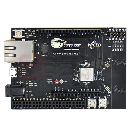


 工商网监
湘ICP备2023018690号
工商网监
湘ICP备2023018690号
