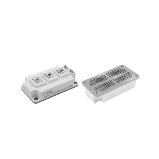
FF3MR12KM1P
62mm�C-Serien�Modul�mit�CoolSiC™�Trench�MOSFET�und�bereits�aufgetragenem�Thermal�Interface
Material
62mm�C-Series�module�with�CoolSiC™�Trench�MOSFET�and�pre-applied�Thermal�Interface�Material
Vorläufige�Daten�/�Preliminary�Data
VDSS = 1200V
ID nom = 375A / IDRM = 750A
Potentielle�Anwendungen
• Anwendungen�mit�hohen�Schaltfrequenzen
• DC/DC�Wandler
• Solar�Anwendungen
• USV-Systeme
Potential�Applications
• High�Frequency�Switching�application
• DC/DC�converter
• Solar�applications
• UPS�systems
Elektrische�Eigenschaften
• Hohe�Stromdichte
• Niedrige�Schaltverluste
Electrical�Features
• High�current�density
• Low�switching�losses
Mechanische�Eigenschaften
• Thermisches Interface Material bereits
aufgetragen
Mechanical�Features
• Pre-applied�Thermal�Interface�Material
Module�Label�Code
Barcode�Code�128
DMX�-�Code
Datasheet
www.infineon.com
Content�of�the�Code
Digit
Module�Serial�Number
Module�Material�Number
Production�Order�Number
Datecode�(Production�Year)
Datecode�(Production�Week)
1�-���5
6�-�11
12�-�19
20�-�21
22�-�23
Please�read�the�Important�Notice�and�Warnings�at�the�end�of�this�document
V�2.0
2020-05-20
�FF3MR12KM1P
Vorläufige�Daten
Preliminary�Data
MOSFET�/�MOSFET
Höchstzulässige�Werte�/�Maximum�Rated�Values
Drain-Source-Spannung
Drain-source�voltage
Drain-Gleichstrom
DC�drain�current
Gepulster�Drainstrom
Pulsed�drain�current
Gate-Source�Spannung
Gate-source�voltage
Tvj = 175°C, VGS = 15 V
Tvj = 25°C
VDSS
�
1200
� V
TH = 60°C
ID nom �
375
� A
ID pulse �
750
� A
-10 / 20
� V
verifiziert�durch�Design,�tp�limitiert�durch�Tvjmax
verified�by�design,�tp�limited�by�Tvjmax
VGSS
�
Charakteristische�Werte�/�Characteristic�Values
min.
Einschaltwiderstand
Drain-source�on�resistance
ID = 375 A
VGS = 15 V
Gate-Schwellenspannung
Gate�threshold�voltage
Gesamt�Gateladung
Total�gate�charge
Interner�Gatewiderstand
Internal�gate�resistor
Eingangskapazität
Input�capacitance
Ausgangskapazität
Output�capacitance
Rückwirkungskapazität
Reverse�transfer�capacitance
COSS�Speicherenergie
COSS�stored�energy
Drain-Source-Reststrom
Zero�gate�voltage�drain�current
Gate-Source-Reststrom
Gate-source�leakage�current
Einschaltverzögerungszeit,�induktive�Last
Turn�on�delay�time,�inductive�load
ID�=�168�mA,�VDS�=�VGS,�Tvj�=�25°C
(tested�after�1ms�pulse�at�VGS�=�+20�V)
Anstiegszeit,�induktive�Last
Rise�time,�inductive�load
Abschaltverzögerungszeit,�induktive�Last
Turn�off�delay�time,�inductive�load
Fallzeit,�induktive�Last
Fall�time,�inductive�load
Einschaltverlustenergie�pro�Puls
Turn-on�energy�loss�per�pulse
Abschaltverlustenergie�pro�Puls
Turn-off�energy�loss�per�pulse
Wärmewiderstand,�Chip�bis�Kühlkörper
Thermal�resistance,�junction�to�heatsink
Tvj = 25°C
Tvj = 125°C
Tvj = 150°C
RDS on
VGS(th)
3,45
typ.
2,83
3,92
4,33
max.
4,50
5,15
mΩ
V
VGS = -5 V / 15 V, VDS = 800 V
QG
1,00
µC
Tvj = 25°C
RGint
1,0
Ω
Ciss
29,8
nF
Coss
1,65
nF
Crss
0,227
nF
Eoss
660
µJ
IDSS
5,40
f = 1 MHz, Tvj = 25°C
VDS = 25 V, VGS = 0 V
f = 1 MHz, Tvj = 25°C
VDS = 25 V, VGS = 0 V
f = 1 MHz, Tvj = 25°C
VDS = 25 V, VGS = 0 V
Tvj = 25°C
VDS = 25 V, VGS = -5 V / 15 V
VDS = 1200 V, VGS = -5 V
Tvj = 25°C
VDS = 0 V
VGS = 20 V
Tvj = 25°C
VGS = -10 V
ID = 375 A, VDS = 600 V
Tvj = 25°C
VGS = -5 V / 15 V
Tvj = 125°C
RGon = 4,30 Ω
Tvj = 150°C
ID = 375 A, VDS = 600 V
Tvj = 25°C
VGS = -5 V / 15 V
Tvj = 125°C
RGon = 4,30 Ω
Tvj = 150°C
ID = 375 A, VDS = 600 V
Tvj = 25°C
VGS = -5 V / 15 V
Tvj = 125°C
RGoff = 3,60 Ω
Tvj = 150°C
ID = 375 A, VDS = 600 V
Tvj = 25°C
VGS = -5 V / 15 V
Tvj = 125°C
RGoff = 3,60 Ω
Tvj = 150°C
ID = 375 A, VDS = 600 V, Lσ = 10 nH
Tvj = 25°C
di/dt = 7,05 kA/µs (Tvj = 150°C)
Tvj = 125°C
VGS = -5 V / 15 V, RGon = 4,30 Ω
Tvj = 150°C
ID = 375 A, VDS = 600 V, Lσ = 10 nH
Tvj = 25°C
du/dt = 7,67 kV/µs (Tvj = 150°C)
Tvj = 125°C
VGS = -5 V / 15 V, RGoff = 3,60 Ω
Tvj = 150°C
pro�MOSFET�/�per�MOSFET
valid�with�IFX�pre-applied�thermal�interface�material
Temperatur�im�Schaltbetrieb
Temperature�under�switching�conditions
520
400
IGSS
79,4
71,6
71,6
198
219
219
69,3
60,4
60,4
51,5
46,8
46,8
18,5
16,0
16,0
13,0
13,5
13,5
td on
tr
td off
tf
Eon
Eoff
RthJH
µA
nA
ns
ns
ns
ns
mJ
mJ
0,140 K/W
Tvj op
-40
150
°C
Body�Diode�/�Body�diode
Höchstzulässige�Werte�/�Maximum�Rated�Values
Body�Diode-Gleichstrom
DC�body�diode�forward�current
Tvj = 175°C, VGS = -5 V
TH = 60°C
ISD
Charakteristische�Werte�/�Characteristic�Values
Durchlassspannung
Forward�voltage
Datasheet
�
min.
ISD = 375 A, VGS = -5 V
ISD = 375 A, VGS = -5 V
ISD = 375 A, VGS = -5 V
Tvj = 25°C
Tvj = 125°C
Tvj = 150°C
2
VSD
� A
120
typ.
4,60
4,35
4,30
max.
5,65
V
V�2.0
2020-05-20
�FF3MR12KM1P
Vorläufige�Daten
Preliminary�Data
Modul�/�Module
Isolations-Prüfspannung
Isolation�test�voltage
RMS, f = 50 Hz, t = 1 min.
VISOL �
4,0
� kV
�
Cu
�
Material�Modulgrundplatte
Material�of�module�baseplate
Innere�Isolation
Internal�isolation
Basisisolierung�(Schutzklasse�1,�EN61140)
basic�insulation�(class�1,�IEC�61140)
�
Al2O3
�
Kriechstrecke
Creepage�distance
Kontakt�-�Kühlkörper�/�terminal�to�heatsink
Kontakt�-�Kontakt�/�terminal�to�terminal
�
29,0
23,0
� mm
Luftstrecke
Clearance
Kontakt�-�Kühlkörper�/�terminal�to�heatsink
Kontakt�-�Kontakt�/�terminal�to�terminal
�
23,0
11,0
� mm
CTI
�
> 400
�
RTI
�
140
Vergleichszahl�der�Kriechwegbildung
Comperative�tracking�index
Relativer�Temperaturindex�(elektr.)
RTI�Elec.
Gehäuse
housing
min.
Modulstreuinduktivität
Stray�inductance�module
Modulleitungswiderstand,�Anschlüsse�Chip
Module�lead�resistance,�terminals�-�chip
TH�=�25°C,�pro�Schalter�/�per�switch
Lagertemperatur
Storage�temperature
20
nH
RCC'+EE'
0,475
mΩ
-40
TBPmax
Anzugsdrehmoment�f.�Modulmontage
Mounting�torque�for�modul�mounting
Schraube�M6��-�Montage�gem.�gültiger�Applikationsschrift
Screw�M6��-�Mounting�according�to�valid�application�note
M
3,00
Anzugsdrehmoment�f.�elektr.�Anschlüsse
Terminal�connection�torque
Schraube�M6��-�Montage�gem.�gültiger�Applikationsschrift
Screw�M6��-�Mounting�according�to�valid�application�note
M
2,5
Gewicht
Weight
max.
LsCE
Tstg
Höchstzulässige
Bodenplattenbetriebstemperatur
Maximum�baseplate�operation�temperature
typ.
� °C
G
340
125
°C
125
°C
6,00
Nm
5,0
Nm
g
Important note: The selection of positive and negative gate-source voltages impacts the long-term behavior of the device. The design
guidelines described in Application Note AN 2018-09 must be considered to ensure sound operation of the device over the planned lifetime.
Storage and shipment of modules with TIM => see AN2012-07
Datasheet
3
V�2.0
2020-05-20
�FF3MR12KM1P
Vorläufige�Daten
Preliminary�Data
Ausgangskennlinie�MOSFET�(typisch)
output�characteristic�MOSFET�(typical)
ID�=�f�(VDS)
VGS�=�15�V
Ausgangskennlinie�MOSFET�(typisch)
output�characteristic�MOSFET�(typical)
ID�=�f�(VDS)
Tvj�=�150°C
750
750
Tvj = 25°C
Tvj = 125°C
Tvj = 150°C
675
600
600
525
525
450
450
ID [A]
ID [A]
675
375
375
300
300
225
225
150
150
75
75
0
0,0
0,5
VGS = 19 V
VGS = 17 V
VGS = 15 V
VGS = 13 V
VGS = 11 V
VGS = 9 V
VGS = 7 V
1,0
1,5
2,0
VDS [V]
2,5
3,0
3,5
0
4,0
Übertragungscharakteristik�MOSFET�(typisch)
transfer�characteristic�MOSFET�(typical)
ID�=�f�(VGS)
VDS�=�20�V
0,0
0,5
1,0
1,5
2,0
2,5 3,0
VDS [V]
3,5
4,0
4,5
5,0
Gateladungs�Charakteristik�MOSFET�(typisch)
gate�charge�characteristic�MOSFET�(typical)
VGS�=�f�(QG)
VDS�=�800�V,�ID�=�375�A,�Tvj�=�25°C
750
15
Tvj = 25°C
Tvj = 125°C
Tvj = 150°C
675
600
10
525
VGS [V]
ID [A]
450
375
5
300
225
0
150
75
0
2
Datasheet
3
4
5
6
7
VGS [V]
8
9
10
-5
11
4
0
200
400
600
QG [nC]
800
1000
V�2.0
2020-05-20
�FF3MR12KM1P
Vorläufige�Daten
Preliminary�Data
Kapazitäts�Charakteristik�MOSFET�(typisch)
capacity�characteristic�MOSFET�(typical)
C�=�f�(VDS)
VGS�=�0�V,�Tvj�=�25°C,�f�=�1�MHz
Schaltverluste�MOSFET�(typisch)
switching�losses�MOSFET�(typical)
Eon�=�f�(ID),�Eoff�=�f�(ID)
VGS�=�-5�V�/�+15�V,�RGon�=�4,3�Ω,�RGoff�=�3,6�Ω,�VDS�=�600�V
100
35
Ciss
Coss
Crss
Eon: Tvj = 125°C, Tvj = 150°C
Eoff: Tvj = 125°C, Tvj = 150°C
30
25
10
C [nF]
E [mJ]
20
15
1
10
5
0,1
0,1
1
10
VDS [V]
100
0
1000
Schaltverluste�MOSFET�(typisch)
switching�losses�MOSFET�(typical)
Eon�=�f�(RG),�Eoff�=�f�(RG)
VGS�=�-5�V�/��+15�V,�ID�=�375�A,�VDS�=�600�V
0
75
150 225 300 375 450 525 600 675 750
ID [A]
Sicherer�Rückwärts-Arbeitsbereich�MOSFET�(RBSOA)
reverse�bias�safe�operating�area�MOSFET�(RBSOA)
ID�=�f�(VDS)
VGS�=�-5�V�/�+15�V,�RGoff�=�3,6�Ω,�TVj�=�150°C
180
825
Eon: Tvj = 125°C, Tvj = 150°C
Eoff: Tvj = 125°C, Tvj = 150°C
750
160
ID: Modul
ID: Chip
675
140
600
525
100
ID [A]
E [mJ]
120
80
450
375
300
60
225
40
150
20
0
75
0
Datasheet
5
10
15
20
25
RG [Ω]
30
35
40
0
45
5
0
200
400
600
800
VDS [V]
1000
1200
1400
V�2.0
2020-05-20
�FF3MR12KM1P
Vorläufige�Daten
Preliminary�Data
Transienter�Wärmewiderstand�MOSFET�
transient�thermal�impedance�MOSFET�
ZthJH�=�f�(t)
1
ZthJH [K/W]
0,1
0,01
i:
1
2
3
4
ri[K/W]: 0,0118 0,0671 0,0457 0,0154
τi[s]:
0,00395 0,0339 0,165 1,32
0,001
0,001
Datasheet
0,01
0,1
t [s]
1
10
6
V�2.0
2020-05-20
�FF3MR12KM1P
Vorläufige�Daten
Preliminary�Data
Schaltplan�/�Circuit�diagram
Gehäuseabmessungen�/�Package�outlines
In fin e o n
Datasheet
7
V�2.0
2020-05-20
�Trademarks
All�referenced�product�or�service�names�and�trademarks�are�the�property�of�their�respective�owners.
�
�
�
Edition�2020-05-20
Published�by
Infineon�Technologies�AG
81726�München,�Germany
©�2020�Infineon�Technologies�AG.
All�Rights�Reserved.
Do�you�have�a�question�about�this�document?
Email:�erratum@infineon.com
�
�
WICHTIGER�HINWEIS
Die�in�diesem�Dokument�enthaltenen�Angaben�stellen�keinesfalls�Garantien�für�die�Beschaffenheit�oder�Eigenschaften�des�Produktes
(“Beschaffenheitsgarantie“)�dar.�Für�Beispiele,�Hinweise�oder�typische�Werte,�die�in�diesem�Dokument�enthalten�sind,�und/oder�Angaben,
die�sich�auf�die�Anwendung�des�Produktes�beziehen,�ist�jegliche�Gewährleistung�und�Haftung�von�Infineon�Technologies�ausgeschlossen,
einschließlich,�ohne�hierauf�beschränkt�zu�sein,�die�Gewähr�dafür,�dass�kein�geistiges�Eigentum�Dritter�verletzt�ist.
Des�Weiteren�stehen�sämtliche,�in�diesem�Dokument�enthaltenen�Informationen,�unter�dem�Vorbehalt�der�Einhaltung�der�in�diesem
Dokument�festgelegten�Verpflichtungen�des�Kunden�sowie�aller�im�Hinblick�auf�das�Produkt�des�Kunden�sowie�die�Nutzung�des�Infineon
Produktes�in�den�Anwendungen�des�Kunden�anwendbaren�gesetzlichen�Anforderungen,�Normen�und�Standards�durch�den�Kunden.
Die�in�diesem�Dokument�enthaltenen�Daten�sind�ausschließlich�für�technisch�geschultes�Fachpersonal�bestimmt.�Die�Beurteilung�der
Eignung�dieses�Produktes�für�die�beabsichtigte�Anwendung�sowie�die�Beurteilung�der�Vollständigkeit�der�in�diesem�Dokument�enthaltenen
Produktdaten�für�diese�Anwendung�obliegt�den�technischen�Fachabteilungen�des�Kunden.
Sollten�Sie�von�uns�weitere�Informationen�im�Zusammenhang�mit�dem�Produkt,�der�Technologie,�Lieferbedingungen�bzw.�Preisen
benötigen,�wenden�Sie�sich�bitte�an�das�nächste�Vertriebsbüro�von�Infineon�Technologies�(www.infineon.com).
WARNHINWEIS
Aufgrund�der�technischen�Anforderungen�können�Produkte�gesundheitsgefährdende�Substanzen�enthalten.�Bei�Fragen�zu�den�in�diesem
Produkt�enthaltenen�Substanzen,�setzen�Sie�sich�bitte�mit�dem�nächsten�Vertriebsbüro�von�Infineon�Technologies�in�Verbindung.
Sofern�Infineon�Technologies�nicht�ausdrücklich�in�einem�schriftlichen,�von�vertretungsberechtigten�Infineon�Mitarbeitern�unterzeichneten
Dokument�zugestimmt�hat,�dürfen�Produkte�von�Infineon�Technologies�nicht�in�Anwendungen�eingesetzt�werden,�in�welchen
vernünftigerweise�erwartet�werden�kann,�dass�ein�Fehler�des�Produktes�oder�die�Folgen�der�Nutzung�des�Produktes�zu
Personenverletzungen�führen.
�
�
�
IMPORTANT�NOTICE
The�information�given�in�this�document�shall�in�no�event�be�regarded�as�a�guarantee�of�conditions�or�characteristics
(“Beschaffenheitsgarantie”).�With�respect�to�any�examples,�hints�or�any�typical�values�stated�herein�and/or�any�information�regarding�the
application�of�the�product,�Infineon�Technologies�hereby�disclaims�any�and�all�warranties�and�liabilities�of�any�kind,�including�without
limitation�warranties�of�non-infringement�of�intellectual�property�rights�of�any�third�party.
In�addition,�any�information�given�in�this�document�is�subject�to�customer’s�compliance�with�its�obligations�stated�in�this�document�and�any
applicable�legal�requirements,�norms�and�standards�concerning�customer’s�products�and�any�use�of�the�product�of�Infineon�Technologies
in�customer’s�applications.
The�data�contained�in�this�document�is�exclusively�intended�for�technically�trained�staff.�It�is�the�responsibility�of�customer’s�technical
departments�to�evaluate�the�suitability�of�the�product�for�the�intended�application�and�the�completeness�of�the�product�information�given�in
this�document�with�respect�to�such�application.
For�further�information�on�the�product,�technology,�delivery�terms�and�conditions�and�prices�please�contact�your�nearest�Infineon
Technologies�office�(www.infineon.com).
WARNINGS
Due�to�technical�requirements�products�may�contain�dangerous�substances.�For�information�on�the�types�in�question�please�contact�your
nearest�Infineon�Technologies�office.
Except�as�otherwise�explicitly�approved�by�Infineon�Technologies�in�a�written�document�signed�by�authorized�representatives�of�Infineon
Technologies,�Infineon�Technologies’�products�may�not�be�used�in�any�applications�where�a�failure�of�the�product�or�any�consequences�of
the�use�thereof�can�reasonably�be�expected�to�result�in�personal�injury.
�