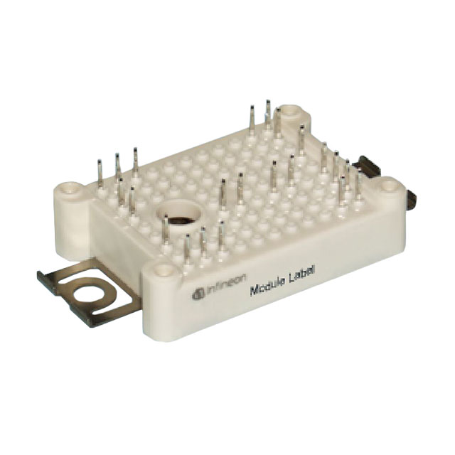
FF45MR12W1M1_B11
EasyDUAL�Modul�mit�CoolSiC™�Trench�MOSFET�und�PressFIT�/�NTC
EasyDUAL�module�with�CoolSiC™�Trench�MOSFET�and�PressFIT�/�NTC
Vorläufige�Daten�/�Preliminary�Data
J
VDSS = 1200V
ID nom = 25A / IDRM = 50A
Potentielle�Anwendungen
• Anwendungen�mit�hohen�Schaltfrequenzen
• DC/DC�Wandler
• Motorantriebe
• USV-Systeme
Potential�Applications
• High�Frequency�Switching�application
• DC/DC�converter
• Motor�drives
• UPS�systems
Elektrische�Eigenschaften
• Niederinduktives�Design
• Niedrige�Schaltverluste
Electrical�Features
• Low�inductive�design
• Low�switching�losses
Mechanische�Eigenschaften
• Integrierter�NTC�Temperatur�Sensor
• PressFIT�Verbindungstechnik
• Robuste Montage durch integrierte
Befestigungsklammern
Mechanical�Features
• Integrated�NTC�temperature�sensor
• PressFIT�contact�technology
• Rugged mounting due to integrated mounting
clamps
Module�Label�Code
Barcode�Code�128
DMX�-�Code
Datasheet
www.infineon.com
Content�of�the�Code
Digit
Module�Serial�Number
Module�Material�Number
Production�Order�Number
Datecode�(Production�Year)
Datecode�(Production�Week)
1�-���5
6�-�11
12�-�19
20�-�21
22�-�23
Please�read�the�Important�Notice�and�Warnings�at�the�end�of�this�document
V�2.2
2020-03-27
�FF45MR12W1M1_B11
Vorläufige�Daten
Preliminary�Data
MOSFET�/�MOSFET
Höchstzulässige�Werte�/�Maximum�Rated�Values
Drain-Source-Spannung
Drain-source�voltage
Drain-Gleichstrom
DC�drain�current
Gepulster�Drainstrom
Pulsed�drain�current
Gate-Source�Spannung
Gate-source�voltage
Tvj = 175°C, VGS = 15 V
1200
� V
ID nom �
25
� A
ID pulse �
50,0
� A
-10 / 20
� V
Tvj = 25°C
VDSS
TH = 75°C
verifiziert�durch�Design,�tp�limitiert�durch�Tvjmax
verified�by�design,�tp�limited�by�Tvjmax
VGSS
�
�
Charakteristische�Werte�/�Characteristic�Values
min.
Einschaltwiderstand
Drain-source�on�resistance
ID = 25 A
VGS = 15 V
Gate-Schwellenspannung
Gate�threshold�voltage
Gesamt�Gateladung
Total�gate�charge
Interner�Gatewiderstand
Internal�gate�resistor
Eingangskapazität
Input�capacitance
Ausgangskapazität
Output�capacitance
Rückwirkungskapazität
Reverse�transfer�capacitance
COSS�Speicherenergie
COSS�stored�energy
Drain-Source-Reststrom
Zero�gate�voltage�drain�current
Gate-Source-Reststrom
Gate-source�leakage�current
Einschaltverzögerungszeit,�induktive�Last
Turn�on�delay�time,�inductive�load
ID�=�10,0�mA,�VDS�=�VGS,�Tvj�=�25°C
(tested�after�1ms�pulse�at�VGS�=�+20�V)
Anstiegszeit,�induktive�Last
Rise�time,�inductive�load
Abschaltverzögerungszeit,�induktive�Last
Turn�off�delay�time,�inductive�load
Fallzeit,�induktive�Last
Fall�time,�inductive�load
Einschaltverlustenergie�pro�Puls
Turn-on�energy�loss�per�pulse
Abschaltverlustenergie�pro�Puls
Turn-off�energy�loss�per�pulse
Kurzschlußverhalten
SC�data
Wärmewiderstand,�Chip�bis�Kühlkörper
Thermal�resistance,�junction�to�heatsink
Tvj = 25°C
Tvj = 125°C
Tvj = 150°C
RDS on
VGS(th)
3,45
typ.
45,0
59,0
66,0
max.
4,50
5,55
mΩ
V
VGS = -5 V / 15 V, VDS = 600 V
QG
0,062
µC
Tvj = 25°C
RGint
4,0
Ω
Ciss
1,84
nF
Coss
0,11
nF
Crss
0,014
nF
Eoss
44,0
µJ
IDSS
0,10
f = 1 MHz, Tvj = 25°C
VDS = 800 V, VGS = 0 V, VAC = 25 mV
f = 1 MHz, Tvj = 25°C
VDS = 800 V, VGS = 0 V, VAC = 25 mV
f = 1 MHz, Tvj = 25°C
VDS = 800 V, VGS = 0 V, VAC = 25 mV
Tvj = 25°C
VDS = 800 V, VGS = -5 V / 15 V
VDS = 1200 V, VGS = -5 V
Tvj = 25°C
VDS = 0 V
Tvj = 25°C
ID = 25 A, VDS = 600 V
VGS = -5 V / 15 V
RGon = 1,00 Ω
ID = 25 A, VDS = 600 V
VGS = -5 V / 15 V
RGon = 1,00 Ω
ID = 25 A, VDS = 600 V
VGS = -5 V / 15 V
RGoff = 1,00 Ω
ID = 25 A, VDS = 600 V
VGS = -5 V / 15 V
RGoff = 1,00 Ω
ID = 25 A, VDS = 600 V, Lσ = 30 nH
di/dt = 5,20 kA/µs (Tvj = 150°C)
VGS = -5 V / 15 V, RGon = 1,00 Ω
ID = 25 A, VDS = 600 V, Lσ = 30 nH
du/dt = 41,6 kV/µs (Tvj = 150°C)
VGS = -5 V / 15 V, RGoff = 1,00 Ω
VGS = 20 V
VGS = -10 V
Tvj = 25°C
Tvj = 125°C
Tvj = 150°C
Tvj = 25°C
Tvj = 125°C
Tvj = 150°C
Tvj = 25°C
Tvj = 125°C
Tvj = 150°C
Tvj = 25°C
Tvj = 125°C
Tvj = 150°C
Tvj = 25°C
Tvj = 125°C
Tvj = 150°C
Tvj = 25°C
Tvj = 125°C
Tvj = 150°C
VGS = -5 V / 15 V, VDD = 800 V
VDSmax = VDSS -LsDS ·di/dt
RG = 10,0 Ω
tP ≤ 2 µs, Tvj = 25°C
tP ≤ 2 µs, Tvj = 150°C
pro�MOSFET�/�per�MOSFET
Temperatur�im�Schaltbetrieb
Temperature�under�switching�conditions
120
400
IGSS
8,20
7,40
7,40
6,30
6,70
6,70
35,2
38,9
38,9
16,4
16,4
16,4
0,30
0,37
0,37
0,033
0,035
0,035
td on
tr
td off
tf
Eon
Eoff
µA
nA
ns
ns
ns
ns
mJ
mJ
ISC
210
205
A
A
RthJH
1,54
K/W
Tvj op
-40
150
°C
Body�Diode�/�Body�diode
Höchstzulässige�Werte�/�Maximum�Rated�Values
Body�Diode-Gleichstrom
DC�body�diode�forward�current
Tvj = 175°C, VGS = -5 V
TH = 75°C
ISD
Charakteristische�Werte�/�Characteristic�Values
Durchlassspannung
Forward�voltage
Datasheet
�
min.
ISD = 25 A, VGS = -5 V
ISD = 25 A, VGS = -5 V
ISD = 25 A, VGS = -5 V
Tvj = 25°C
Tvj = 125°C
Tvj = 150°C
2
VSD
� A
8
typ.
4,60
4,35
4,30
max.
5,65
V
V�2.2
2020-03-27
�FF45MR12W1M1_B11
Vorläufige�Daten
Preliminary�Data
NTC-Widerstand�/�NTC-Thermistor
Charakteristische�Werte�/�Characteristic�Values
min.
typ.
max.
Nennwiderstand
Rated�resistance
TNTC = 25°C
Abweichung�von�R100
Deviation�of�R100
TNTC = 100°C, R100 = 493 Ω
Verlustleistung
Power�dissipation
TNTC = 25°C
B-Wert
B-value
R2 = R25 exp [B25/50(1/T2 - 1/(298,15 K))]
B25/50
3375
K
B-Wert
B-value
R2 = R25 exp [B25/80(1/T2 - 1/(298,15 K))]
B25/80
3411
K
B-Wert
B-value
R2 = R25 exp [B25/100(1/T2 - 1/(298,15 K))]
B25/100
3433
K
R25
5,00
∆R/R
-5
P25
kΩ
5
%
20,0
mW
Angaben�gemäß�gültiger�Application�Note.
Specification�according�to�the�valid�application�note.
Modul�/�Module
Isolations-Prüfspannung
Isolation�test�voltage
RMS, f = 50 Hz, t = 1 min.
Innere�Isolation
Internal�isolation
Basisisolierung�(Schutzklasse�1,�EN61140)
basic�insulation�(class�1,�IEC�61140)
�
Al2O3
�
Kriechstrecke
Creepage�distance
Kontakt�-�Kühlkörper�/�terminal�to�heatsink
Kontakt�-�Kontakt�/�terminal�to�terminal
�
11,5
6,3
� mm
Luftstrecke
Clearance
Kontakt�-�Kühlkörper�/�terminal�to�heatsink
Kontakt�-�Kontakt�/�terminal�to�terminal
�
10,0
5,0
� mm
CTI
�
> 200
�
RTI
�
140
VISOL �
Vergleichszahl�der�Kriechwegbildung
Comperative�tracking�index
Relativer�Temperaturindex�(elektr.)
RTI�Elec.
Gehäuse
housing
� kV
3,0
min.
Modulstreuinduktivität
Stray�inductance�module
LsCE
Lagertemperatur
Storage�temperature
Tstg
-40
Anpresskraft für mech. Bef. pro Feder
mountig force per clamp
F
20
Gewicht
Weight
G
typ.
� °C
max.
18
24
nH
125
°C
50
N
g
The current under continuous operation is limited to 25 A rms per connector pin.
Important note: The selection of positive and negative gate-source voltages impacts the long-term behavior of the device. The design
guidlines described in Application Note AN 2018-09 must be considered to ensure sound operation of the device over the planned lifetime.
Datasheet
3
V�2.2
2020-03-27
�FF45MR12W1M1_B11
Vorläufige�Daten
Preliminary�Data
Ausgangskennlinie�MOSFET�(typisch)
output�characteristic�MOSFET�(typical)
ID�=�f�(VDS)
VGS�=�15�V
Übertragungscharakteristik�MOSFET�(typisch)
transfer�characteristic�MOSFET�(typical)
ID�=�f�(VGS)
VDS�=�20�V
50
50
TVj = 25 °C
TVj = 125 °C
TVj = 150 °C
45
40
40
35
35
30
30
ID [A]
ID [A]
45
Tvj = 25 °C
25
25
20
20
15
15
10
10
5
5
0
0,0
0,5
1,0
1,5
2,0
VDS [V]
2,5
3,0
3,5
0
4,0
Schaltzeiten�MOSFET�(typisch)
switching�times�MOSFET�(typical)
tdon�=�f�(ID),�tr�=�f�(ID),�tdoff�=�f�(ID),�tf�=�f�(ID)
VGS�=�-5�V�/�15�V,�RGon�=�1�Ω,�RGoff�=�1�Ω,�VDS�=�600�V,�Tvj�=�150°C
3
4
5
6
7
8
VGS [V]
9
10
11
12
9
10
Schaltzeiten�MOSFET�(typisch)
switching�times�MOSFET�(typical)
tdon�=�f�(RG),�tr�=�f�(RG),�tdoff�=�f�(RG),�tf�=�f�(RG)
VGS�=�-5�V�/�15�V,�ID�=�25�A,�VDS�=�600�V,�Tvj�=�150°C
1
1
tdon
tr
tdoff
tf
tdon
tr
tdoff
tf
t [µs]
0,1
t [µs]
0,1
0,01
0,001
0,01
0
Datasheet
5
10
15
20
25 30
ID [A]
35
40
45
50
0,001
4
0
1
2
3
4
5
6
RG [Ohm]
7
8
V�2.2
2020-03-27
�FF45MR12W1M1_B11
Vorläufige�Daten
Preliminary�Data
Schaltverluste�MOSFET�(typisch)
switching�losses�MOSFET�(typical)
Eon�=�f�(ID),�Eoff�=�f�(ID)
VGS�=�-5�V�/�15�V,�RGon�=�1�Ω,�RGoff�=�1�Ω,�VDS�=�600�V
Schaltverluste�MOSFET�(typisch)
switching�losses�MOSFET�(typical)
Eon�=�f�(RG),�Eoff�=�f�(RG)
VGS�=�-5�V�/�15�V,�ID�=�25�A,�VDS�=�600�V
0,70
0,70
Eon, Tvj = 125°C, Eon, Tvj = 150°C,
Eoff, Tvj = 125°C, Eoff, Tvj = 150°C,
Eon, Tvj = 125°C, Eon, Tvj = 150°C
Eoff, Tvj = 125°C, Eoff, Tvj = 150°C
0,50
0,50
0,40
0,40
E [mJ]
0,60
E [mJ]
0,60
0,30
0,30
0,20
0,20
0,10
0,10
0,00
0
5
10
15
20
25 30
ID [A]
35
40
45
0,00
50
Sicherer�Rückwärts-Arbeitsbereich�MOSFET�(RBSOA)
reverse�bias�safe�operating�area�MOSFET�(RBSOA)
ID�=�f�(VDS)
VGS�=�-�5�V�/�15�V,�Tvj�=�150°C,�RG�=�1�Ω
0
1
2
3
4
5
6
RG [Ω]
7
8
9
10
Transienter�Wärmewiderstand�MOSFET�
transient�thermal�impedance�MOSFET�
ZthJH�=�f�(t)
55
10
ID, Modul
ID, Chip
50
Zth: MOSFET
45
1
40
ZthJH [K/W]
ID [A]
35
30
25
0,1
20
15
0,01
10
i:
1
2
3
4
ri[K/W]: 0,076
0,221
0,453 0,79
τi[s]:
0,000603 0,00674 0,0363 0,161
5
0
0
Datasheet
200
400
600
800
VDS [V]
1000
1200
1400
0,001
0,001
5
0,01
0,1
t [s]
1
10
V�2.2
2020-03-27
�FF45MR12W1M1_B11
Vorläufige�Daten
Preliminary�Data
NTC-Widerstand-Temperaturkennlinie�(typisch)
NTC-Thermistor-temperature�characteristic�(typical)
R�=�f�(T)
100000
Rtyp
R[Ω]
10000
1000
100
0
Datasheet
20
40
60
80
100
TNTC [°C]
120
140
160
6
V�2.2
2020-03-27
�FF45MR12W1M1_B11
Vorläufige�Daten
Preliminary�Data
Schaltplan�/�Circuit�diagram
J
Gehäuseabmessungen�/�Package�outlines
Infineon
Datasheet
7
V�2.2
2020-03-27
�Trademarks
All referenced product or service names and trademarks are the property of their respective owners.
Edition 2020-03-27
Published by
Infineon Technologies AG
81726 München, Germany
© 2020 Infineon Technologies AG.
All Rights Reserved.
Do you have a question about this document?
Email: erratum@infineon.com
WICHTIGER HINWEIS
Die in diesem Dokument enthaltenen Angaben stellen keinesfalls Garantien für die Beschaffenheit oder Eigenschaften des Produktes
(“Beschaffenheitsgarantie“) dar. Für Beispiele, Hinweise oder typische Werte, die in diesem Dokument enthalten sind, und/oder Angaben,
die sich auf die Anwendung des Produktes beziehen, ist jegliche Gewährleistung und Haftung von Infineon Technologies ausgeschlossen,
einschließlich, ohne hierauf beschränkt zu sein, die Gewähr dafür, dass kein geistiges Eigentum Dritter verletzt ist.
Des Weiteren stehen sämtliche, in diesem Dokument enthaltenen Informationen, unter dem Vorbehalt der Einhaltung der in diesem
Dokument festgelegten Verpflichtungen des Kunden sowie aller im Hinblick auf das Produkt des Kunden sowie die Nutzung des Infineon
Produktes in den Anwendungen des Kunden anwendbaren gesetzlichen Anforderungen, Normen und Standards durch den Kunden.
Die in diesem Dokument enthaltenen Daten sind ausschließlich für technisch geschultes Fachpersonal bestimmt. Die Beurteilung der
Eignung dieses Produktes für die beabsichtigte Anwendung sowie die Beurteilung der Vollständigkeit der in diesem Dokument enthaltenen
Produktdaten für diese Anwendung obliegt den technischen Fachabteilungen des Kunden.
Sollten Sie von uns weitere Informationen im Zusammenhang mit dem Produkt, der Technologie, Lieferbedingungen bzw. Preisen
benötigen, wenden Sie sich bitte an das nächste Vertriebsbüro von Infineon Technologies (www.infineon.com).
WARNHINWEIS
Aufgrund der technischen Anforderungen können Produkte gesundheitsgefährdende Substanzen enthalten. Bei Fragen zu den in diesem
Produkt enthaltenen Substanzen, setzen Sie sich bitte mit dem nächsten Vertriebsbüro von Infineon Technologies in Verbindung.
Sofern Infineon Technologies nicht ausdrücklich in einem schriftlichen, von vertretungsberechtigten Infineon Mitarbeitern unterzeichneten
Dokument zugestimmt hat, dürfen Produkte von Infineon Technologies nicht in Anwendungen eingesetzt werden, in welchen
vernünftigerweise erwartet werden kann, dass ein Fehler des Produktes oder die Folgen der Nutzung des Produktes zu
Personenverletzungen führen.
IMPORTANT NOTICE
The information given in this document shall in no event be regarded as a guarantee of conditions or characteristics
(“Beschaffenheitsgarantie”). With respect to any examples, hints or any typical values stated herein and/or any information regarding the
application of the product, Infineon Technologies hereby disclaims any and all warranties and liabilities of any kind, including without
limitation warranties of non-infringement of intellectual property rights of any third party.
In addition, any information given in this document is subject to customer’s compliance with its obligations stated in this document and any
applicable legal requirements, norms and standards concerning customer’s products and any use of the product of Infineon Technologies
in customer’s applications.
The data contained in this document is exclusively intended for technically trained staff. It is the responsibility of customer’s technical
departments to evaluate the suitability of the product for the intended application and the completeness of the product information given in
this document with respect to such application.
For further information on the product, technology, delivery terms and conditions and prices please contact your nearest Infineon
Technologies office (www.infineon.com).
WARNINGS
Due to technical requirements products may contain dangerous substances. For information on the types in question please contact your
nearest Infineon Technologies office.
Except as otherwise explicitly approved by Infineon Technologies in a written document signed by authorized representatives of Infineon
Technologies, Infineon Technologies’ products may not be used in any applications where a failure of the product or any consequences of
the use thereof can reasonably be expected to result in personal injury.
�


 工商网监
湘ICP备2023018690号
工商网监
湘ICP备2023018690号
