V er s io n 2.3 , 2 2 M ar c h 2 01 0
CCM-PFC
ICE 2 PCS 0 1
ICE 2 PCS 0 1G
St a n d a lo n e P o w e r F a ct o r
Co r r e c tio n ( P FC ) C o n tr o lle r in
Co n ti n u o u s Co n d u c t io n Mo d e
( CC M )
Po we r M a na g e me n t & Su p ply
N e v e r
s t o p
t h i n k i n g .
�CCM-PFC
Revision History:
2010-03-22
Datasheet
Previous Version: V 2.1
Page
18&19
Subjects (major changes since last revision)
Package outline dimension changed
For questions on technology, delivery and prices please contact the Infineon Technologies Offices in Germany or
the Infineon Technologies Companies and Representatives worldwide: see our webpage at http://
www.infineon.com
CoolMOST™, CoolSET™ are trademarks of Infineon Technologies AG.
Edition 2010-03-22
Published by
Infineon Technologies AG
81726 München, Germany
© 2007 Infineon Technologies AG
All Rights Reserved.
Legal Disclaimer
The information given in this document shall in no event be regarded as a guarantee of conditions or
characteristics. With respect to any examples or hints given herein, any typical values stated herein and/or any
information regarding the application of the device, Infineon Technologies hereby disclaims any and all warranties
and liabilities of any kind, including without limitation, warranties of non-infringement of intellectual property rights
of any third party.
Information
For further information on technology, delivery terms and conditions and prices please contact your nearest
Infineon Technologies Office (www.infineon.com).
Warnings
Due to technical requirements components may contain dangerous substances. For information on the types in
question please contact your nearest Infineon Technologies Office.
Infineon Technologies Components may be used in life-support devices or systems only with the express written
approval of Infineon Technologies, if a failure of such components can reasonably be expected to cause the failure
of that life-support device or system, or to affect the safety or effectiveness of that device or system. Life support
devices or systems are intended to be implanted in the human body, or to support and/or maintain and sustain
and/or protect human life. If they fail, it is reasonable to assume that the health of the user or other persons may
be endangered.
�CCM-PFC
ICE2PCS01
ICE2PCS01G
Standalone Power Factor Correction
(PFC) Controller in Continuous
Conduction Mode (CCM)
ICE2PCS01
PG-DIP-8
Product Highlights
•
•
•
•
•
•
•
Leadfree DIP and DSO Package
Wide Input Range
Optimized for applications which require fast Startup
Output Power Controllable by External Sense Resistor
Programmable Operating Frequency
Output Over-Voltage Protection
Fast Output Dynamic Response during Load Jumps
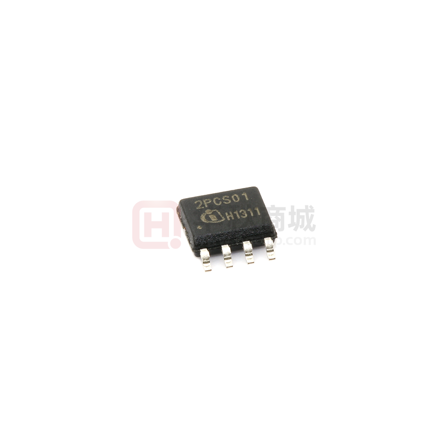
ICE2PCS01G
PG-DSO-8
Features
Description
•
•
•
•
The ICE2PCS01/G is a 8-pin wide input range controller
IC for active power factor correction converters. It is designed for converters in boost topology, and requires few
external components. Its power supply is recommended
to be provided by an external auxiliary supply which will
switch on and off the IC.
The IC operates in the CCM with average current control,
and in DCM only under light load condition. The switching
frequency is programmable by the resistor at pin 4. Both
compensations for the current and voltage loop are external to allow full user control.
There are various protection features incorporated to ensure safe system operation conditions. The internal reference is trimmed (3V+2%) to ensure precise protection and
control level. The device has a fast startup time with controlled peak start up current.
•
•
•
•
•
•
•
•
•
•
•
•
Ease of Use with Few External Components
Supports Wide Range
Average Current Control
External Current and Voltage Loop Compensation
for Greater User Flexibility
Programmable Operating/Switching Frequency
(50kHz - 250kHz)
Max Duty Cycle of 95% (at 25°C) at 125kHz
Trimmed Internal Reference Voltage (3V+2% at
25°C)
VCC Under-Voltage Lockout
Cycle by Cycle Peak Current Limiting
Output Over-Voltage Protection
Open Loop Detection
Enhanced Dynamic Response
Short Startup(SoftStart) duration
Fulfills Class D Requirements of IEC 1000-3-2
Soft Overcurrent Protection
Typical Application
VOUT
Auxiliary Supply
85 ... 265 VAC
EMI-Filter
VCC
SWITCH
ICE2PCS01/
ICE2PCS01G
PFC-Controller
Protection Unit
GATE
FREQ
ICOMP
PWM Logic
Driver
Variable
Oscillator
Current Loop
Compensation
ISENSE
Type
Package
ICE2PCS01
PG-DIP-8
ICE2PCS01G
PG-DSO-8
Version 2.3
Voltage Loop
Compensation
Ramp
Generator
VSENSE
VCOMP
Nonlinear
Gain
GND
3
22 March 2010
�CCM-PFC
ICE2PCS01/G
1
1.1
1.2
Pin Configuration and Functionality . . . . . . . . . . . . . . . . . . . . . . . . . . . . . 5
Pin Configuration . . . . . . . . . . . . . . . . . . . . . . . . . . . . . . . . . . . . . . . . . . . . . . 5
Pin Functionality . . . . . . . . . . . . . . . . . . . . . . . . . . . . . . . . . . . . . . . . . . . . . . 5
2
Representative Block diagram . . . . . . . . . . . . . . . . . . . . . . . . . . . . . . . . . . 6
3
3.1
3.2
3.3
3.4
3.4.1
3.4.2
3.4.3
3.4.4
3.5
3.6
3.6.1
3.6.2
3.6.3
3.6.4
3.7
3.8
3.8.1
3.8.2
3.9
Functional Description . . . . . . . . . . . . . . . . . . . . . . . . . . . . . . . . . . . . . . . . 7
General . . . . . . . . . . . . . . . . . . . . . . . . . . . . . . . . . . . . . . . . . . . . . . . . . . . . . 7
Power Supply . . . . . . . . . . . . . . . . . . . . . . . . . . . . . . . . . . . . . . . . . . . . . . . . 7
Start-up . . . . . . . . . . . . . . . . . . . . . . . . . . . . . . . . . . . . . . . . . . . . . . . . . . . . . 7
System Protection . . . . . . . . . . . . . . . . . . . . . . . . . . . . . . . . . . . . . . . . . . . . . 8
Soft Over Current Control (SOC) . . . . . . . . . . . . . . . . . . . . . . . . . . . . . . . 8
Peak Current Limit (PCL) . . . . . . . . . . . . . . . . . . . . . . . . . . . . . . . . . . . . . 9
Open Loop Protection / Input Under Voltage Protect (OLP) . . . . . . . . . . . 9
Over-Voltage Protection (OVP) . . . . . . . . . . . . . . . . . . . . . . . . . . . . . . . . . 9
Frequency Setting . . . . . . . . . . . . . . . . . . . . . . . . . . . . . . . . . . . . . . . . . . . . . 9
Average Current Control . . . . . . . . . . . . . . . . . . . . . . . . . . . . . . . . . . . . . . . 10
Complete Current Loop . . . . . . . . . . . . . . . . . . . . . . . . . . . . . . . . . . . . . . 10
Current Loop Compensation . . . . . . . . . . . . . . . . . . . . . . . . . . . . . . . . . . 10
Pulse Width Modulation (PWM) . . . . . . . . . . . . . . . . . . . . . . . . . . . . . . . 10
Nonlinear Gain Block . . . . . . . . . . . . . . . . . . . . . . . . . . . . . . . . . . . . . . . 10
PWM Logic . . . . . . . . . . . . . . . . . . . . . . . . . . . . . . . . . . . . . . . . . . . . . . . . . 11
Voltage Loop . . . . . . . . . . . . . . . . . . . . . . . . . . . . . . . . . . . . . . . . . . . . . . . . 11
Voltage Loop Compensation . . . . . . . . . . . . . . . . . . . . . . . . . . . . . . . . . . 11
Enhanced Dynamic Response . . . . . . . . . . . . . . . . . . . . . . . . . . . . . . . . 11
Output Gate Driver . . . . . . . . . . . . . . . . . . . . . . . . . . . . . . . . . . . . . . . . . . . 11
4
4.1
4.2
4.3
4.3.1
4.3.2
4.3.3
4.3.4
4.3.5
4.3.6
4.3.7
Electrical Characteristics . . . . . . . . . . . . . . . . . . . . . . . . . . . . . . . . . . . . . 13
Absolute Maximum Ratings . . . . . . . . . . . . . . . . . . . . . . . . . . . . . . . . . . . . 13
Operating Range . . . . . . . . . . . . . . . . . . . . . . . . . . . . . . . . . . . . . . . . . . . . . 13
Characteristics . . . . . . . . . . . . . . . . . . . . . . . . . . . . . . . . . . . . . . . . . . . . . . 14
Supply Section . . . . . . . . . . . . . . . . . . . . . . . . . . . . . . . . . . . . . . . . . . . . 14
Variable Frequency Section . . . . . . . . . . . . . . . . . . . . . . . . . . . . . . . . . . 14
PWM Section . . . . . . . . . . . . . . . . . . . . . . . . . . . . . . . . . . . . . . . . . . . . . 15
System Protection Section . . . . . . . . . . . . . . . . . . . . . . . . . . . . . . . . . . . 15
Current Loop Section . . . . . . . . . . . . . . . . . . . . . . . . . . . . . . . . . . . . . . . 16
Voltage Loop Section . . . . . . . . . . . . . . . . . . . . . . . . . . . . . . . . . . . . . . . 16
Driver Section . . . . . . . . . . . . . . . . . . . . . . . . . . . . . . . . . . . . . . . . . . . . . 17
5
Outline Dimension . . . . . . . . . . . . . . . . . . . . . . . . . . . . . . . . . . . . . . . . . . 18
Version 2.3
4
22 March 2010
�CCM-PFC
ICE2PCS01/G
Pin Configuration and Functionality
1
Pin Configuration and Functionality
1.1
Pin Configuration
Pin
ICOMP (Current Loop Compensation)
Low pass filter and compensation of the current control
loop. The capacitor which is connected at this pin
integrates the output current of OTA2 and averages the
current sense signal.
Symbol
Function
1
GND
IC Ground
2
ICOMP
Current Loop Compensation
3
ISENSE
Current Sense Input
4
FREQ
Switching Frequency Setting
5
VCOMP
Voltage Loop Compensation
6
VSENSE VOUT Sense (Feedback) Input
7
VCC
IC Supply Voltage
8
GATE
Gate Drive Output
ISENSE (Current Sense Input)
The ISENSE Pin senses the voltage drop at the
external sense resistor (R1). This is the input signal for
the average current regulation in the current loop. It is
also fed to the peak current limitation block.
During power up time, high inrush currents cause high
negative voltage drop at R1, driving currents out of pin
3 which could be beyond the absolute maximum
ratings. Therefore a series resistor (R2) of around
220W is recommended in order to limit this current into
the IC.
FREQ (Frequency Setting)
This pin allows the setting of the operating switching
frequency by connecting a resistor to ground. The
frequency range is from 50kHz to 250kHz.
Package PG-DIP-8 / PG-DSO-8
GND
1
8
GATE
ICOMP
2
7
VCC
ISENSE
3
6
VSENSE
FREQ
4
5
VCOMP
Figure 1
1.2
VSENSE (Voltage Sense/Feedback)
The output bus voltage is sensed at this pin via a
resistive divider. The reference voltage for this pin is
3V.
VCOMP (Voltage Loop Compensation)
This pin provides the compensation of the output
voltage loop with a compensation network to ground
(see Figure 2). This also gives the soft start function
which controls an increasing AC input current during
start-up.
VCC (Power Supply)
The VCC pin is the positive supply of the IC and should
be connected to an external auxiliary supply. The
operating range is between 11V and 26V. The turn-on
threshold is at 11.8V and under voltage occurs at 11V.
There is no internal clamp for a limitation of the power
supply.
Pin Configuration (top view)
GATE
The GATE pin is the output of the internal driver stage,
which has a capability of 1.5A instantaneous source
and 2.0A instantaneous sink current.
Its gate drive voltage is clamped at 15V (typically).
Pin Functionality
GND (Ground)
The ground potential of the IC.
Version 2.3
5
22 March 2010
�CCM-PFC
ICE2PCS01/G
Representative Block diagram
2
Figure 2
Representative Block diagram
Representative Block diagram
Version 2.3
6
22 March 2010
�CCM-PFC
ICE2PCS01/G
Functional Description
3
Functional Description
3.1
General
If VCC drops below 11V, the IC is off. The IC will then
be consuming typically 300mA, whereas consuming
13mA during normal operation.
The IC can be turned off and forced into standby mode
by pulling down the voltage at pin 6 (VSENSE) to lower
than 0.6V. The current consumption is reduced to
300µA in this mode.
The ICE2PCS01/G is a 8 pin control IC for power factor
correction converters. It comes in both DIP and DSO
packages and is suitable for wide range line input
applications from 85 to 265 VAC. The IC supports
converters in boost topology and it operates in
continuous conduction mode (CCM) with average
current control.
The IC operates with a cascaded control; the inner
current loop and the outer voltage loop. The inner
current loop of the IC controls the sinusoidal profile for
the average input current. It uses the dependency of
the PWM duty cycle on the line input voltage to
determine the corresponding input current. This means
the average input current follows the input voltage as
long as the device operates in CCM. Under light load
condition, depending on the choke inductance, the
system may enter into discontinuous conduction mode
(DCM). In DCM, the average current waveform will be
distorted but the resultant harmonics are still low
enough to meet the Class D requirement of IEC 10003-2.
The outer voltage loop controls the output bus voltage.
Depending on the load condition, OTA1 establishes an
appropriate voltage at VCOMP pin which controls the
amplitude of the average input current.
The IC is equipped with various protection features to
ensure safe operating condition for both the system
and device. Important protection features are namely
Open-Loop protection, Current Limitation and Output
Over-voltage Protection.
3.3
Start-up
Figure 4 shows the operation of voltage loop’s OTA1
during startup. The VCOMP pin is pull internally to
ground via switch S1 during UVLO and other fault
conditions (see later section on “System Protection”).
During power up when VOUT is less than 83% of the
rated level, OTA1 sources an output current, maximum
30mA, into the compensation network at pin 5
(VCOMP) causing the voltage at this pin to rise linearly.
This results in a controlled linear increase of the input
current from 0A thus reducing the stress on the
external component.
VSENSE
R4
x V OUT )
R3 + R4
(
OTA1
3V
VCOMP
S1
3.2
R6
Power Supply
C4
An internal under voltage lockout (UVLO) block
monitors the VCC power supply. As soon as it exceeds
11.8V and the voltage at pin 6 (VSENSE) is >0.6V, the
IC begins operating its gate drive and performs its
Startup as shown in Figure 3.
.
(VVSENSE > 0.6 V)
(VVSENSE < 0.6 V)
p ro tec t
Figure 4
C5
IC E 2 P C S 0 1 /G
Startup Circuit
As VOUT has not reached within 5% from the rated
value, VCOMP voltage is level-shifted by the window
detect block as shown in Figure 5, to ensure there is
fast boost up of the output voltage.
When VOUT approaches its rated value, OTA1’s
sourcing current drops and the level shift of the window
detect block is removed. The normal voltage loop then
takes control.
(VVSENSE > 0.6 V)
VCC
11.8 V
11.0 V
t
IC's
Start Normal
Open loop/
OFF
Up Operation
Standby
State
Figure 3
Normal
Operation
OFF
State of Operation respect to VCC
Version 2.3
7
22 March 2010
�CCM-PFC
ICE2PCS01/G
Functional Description
3.4
Window Detect
The IC provides several protection features in order to
ensure the PFC system in safe operating range.
Depending on the input line voltage (VIN) and output
bus voltage (VOUT), Figure 7 and 8 show the conditions
when these protections are active.
Normal Control
Max Vcomp current
VOUT =rated
VOUT
System Protection
95%rated
83%rated
VCC > VCCUVLO
VCC400kW
Clamped at 15V if driven
internally.
1)
According to EIA/JESD22-A114-B (discharging a 100pF capacitor through a 1.5kW series resistor)
2)
Absolute ISENSE current should not be exceeded
4.2
Note:
Operating Range
Within the operating range the IC operates as described in the functional description.
Parameter
Symbol
Limit Values
min.
Unit
max.
VCC Supply Voltage
VCC
VCCUVLO 25
V
Junction Temperature
TJCon
-40
°C
Version 2.3
13
Remarks
125
22 March 2010
�CCM-PFC
ICE2PCS01/G
Electrical Characteristics
4.3
Note:
4.3.1
Characteristics
The electrical characteristics involve the spread of values within the specified supply voltage and junction
temperature range TJ from – 40 °C to 125°C.Typical values represent the median values, which are
related to 25°C. If not otherwise stated, a supply voltage of VCC =18V is assumed for test condition.
Supply Section
Parameter
Symbol
Limit Values
min.
typ.
Unit Test Condition
max.
VCC Turn-On Threshold
VCCon
11.4
11.8
12.7
V
VCC Turn-Off Threshold/
Under Voltage Lock Out
VCCUVLO
10.4
11.0
11.7
V
VCC Turn-On/Off Hysteresis
VCChy
0.65
0.8
1.4
V
Start Up Current
Before VCCon
ICCstart
-
450
1100
mA
VVCC=VVCCon -0.1V
Operating Current with active GATE
ICCHG
-
15
20
mA
R5 = 33kW
CL= 4.7nF
Operating Current during Standby
ICCStdby
-
700
1300
mA
VVSENSE= 0.5V
VICOMP= 4V
4.3.2
Variable Frequency Section
Parameter
Symbol
Limit Values
min.
typ.
Unit Test Condition
max.
Switching Frequency (Typical)
FSWnom
124
136
147
kHz
R5 = 33kW
Switching Frequency (Min.)
FSWmin
50
56
62
kHz
R5 = 82kW
Switching Frequency (Max.)
FSWmax
250
285
315
kHz
R5 = 15kW
Voltage at FREQ pin
VFREQ
1.65
1.70
1.76
V
Version 2.3
14
22 March 2010
�CCM-PFC
ICE2PCS01/G
Electrical Characteristics
4.3.3
PWM Section
Parameter
Symbol
Max. Duty Cycle
DMAX
Min. Duty Cycle
DMIN
Min. Off Time
TOFFMIN
Limit Values
Unit Test Condition
min.
typ.
max.
92
95
98.5
%
FSW = FSWnom
(R5 = 33kW)
0
%
VVCOMP= 0V, VVSENSE= 3V
VICOMP= 4.3V
580
ns
VVSENSE= 3V
VISENSE= 0.1V (R5 = 33kW)
100
250
The parameter is not subject to production test - verified by design/characterization
4.3.4
System Protection Section
Parameter
Symbol
Limit Values
min.
typ.
Unit Test Condition
max.
Open Loop Protection (OLP)
VSENSE Threshold
VOLP
0.55
0.6
0.65
V
Peak Current Limitation (PCL)
ISENSE Threshold
VPCL
-1.16
-1.04
-0.95
V
Soft Over Current Control (SOC)
ISENSE Threshold
VSOC
-0.75
-0.68
-0.61
V
Output Over-Voltage Protection (OVP)
VOVP
3.1
3.25
3.4
V
Version 2.3
15
22 March 2010
�CCM-PFC
ICE2PCS01/G
Electrical Characteristics
4.3.5
Current Loop Section
Parameter
Symbol
Limit Values
min.
OTA2 Transconductance Gain
typ.
Unit Test Condition
max.
GmOTA2
0.8
1.0
1.3
mS
OTA2 Output Linear Range1)
IOTA2
-
± 50
-
mA
ICOMP Voltage during OLP
VICOMPF
3.9
4.2
-
V
4.3.6
At Temp = 25°C
VVSENSE= 0.5V
Voltage Loop Section
Parameter
Symbol
Limit Values
min.
OTA1 Reference Voltage
typ.
Unit Test Condition
max.
VOTA1
2.92
3.00
3.08
V
OTA1 Transconductance Gain
GmOTA1
26
39
51
mS
OTA1 Max. Source Current
Under Normal Operation
IOTA1SO
18
30
38
mA
VVSENSE= 2V
VVCOMP= 3V
OTA1 Max. Sink Current
Under Normal Operation
IOTA1SK
21
30
41
mA
VVSENSE= 4V
VVCOMP= 3V
VHi
VLo
3.09
2.76
3.18
2.85
3.26
2.94
V
V
VSENSE Input Bias Current at 3V
IVSEN3V
0
-
1.5
mA
VVSENSE= 3V
VSENSE Input Bias Current at 1V
IVSEN1V
0
-
1
mA
VVSENSE= 1V
VVCOMPF
0
0.2
0.4
V
VVSENSE= 0.5V
IVCOMP= 0.5mA
Enhanced Dynamic Response
VSENSE High Threshold
VSENSE Low Threshold
VCOMP Voltage during OLP
Version 2.3
16
measured at VSENSE
22 March 2010
�CCM-PFC
ICE2PCS01/G
Electrical Characteristics
4.3.7
Driver Section
Parameter
Symbol
GATE Low Voltage
Limit Values
min.
typ.
max.
-
-
1.2
V
VCC =10V
IGATE = 5 mA
1.5
V
VCC =10V
IGATE =20 mA
VGATEL
-
GATE High Voltage
Unit Test Condition
VGATEH
-
0.4
-
V
IGATE = 0 A
-
-
1.0
V
IGATE = 20 mA
-0.2
0
-
V
IGATE = -20 mA
-
14.8
-
V
VCC = 25V
CL = 4.7nF
-
14.8
-
V
VCC = 19V
CL = 4.7nF
7.8
9.2
-
V
VCC = VVCCoff + 0.2V
CL = 4.7nF
GATE Rise Time
tr
-
60
-
ns
VGate = 2V ...12V
CL = 4.7nF
GATE Fall Time
tf
-
50
-
ns
VGate = 12V ...2V
CL = 4.7nF
GATE Current, Peak,
Rising Edge
IGATE
-1.5
-
-
A
CL = 4.7nF1)
GATE Current, Peak,
Falling Edge
IGATE
-
-
2.0
A
CL = 4.7nF1)
1)
Design characteristics (not meant for production testing)
Version 2.3
17
22 March 2010
�CCM-PFC
ICE2PCS01/G
Outline Dimension
5
Outline Dimension
PG-DIP-8 Outline Dimension
Version 2.3
18
22 March 2010
�CCM-PFC
ICE2PCS01/G
Outline Dimension
PG-DSO-8 Outline Dimension
Version 2.3
19
22 March 2010
�Total Quality Management
Qualität hat für uns eine umfassende
Bedeutung. Wir wollen allen Ihren
Ansprüchen in der bestmöglichen
Weise gerecht werden. Es geht uns also
nicht nur um die Produktqualität –
unsere Anstrengungen gelten
gleichermaßen der Lieferqualität und
Logistik, dem Service und Support
sowie allen sonstigen Beratungs- und
Betreuungsleistungen.
Quality takes on an allencompassing
significance at Semiconductor Group.
For us it means living up to each and
every one of your demands in the best
possible way. So we are not only
concerned with product quality. We
direct our efforts equally at quality of
supply and logistics, service and
support, as well as all the other ways in
which we advise and attend to you.
Dazu gehört eine bestimmte
Geisteshaltung unserer Mitarbeiter.
Total Quality im Denken und Handeln
gegenüber Kollegen, Lieferanten und
Ihnen, unserem Kunden. Unsere
Leitlinie ist jede Aufgabe mit „Null
Fehlern“ zu lösen – in offener
Sichtweise auch über den eigenen
Arbeitsplatz hinaus – und uns ständig
zu verbessern.
Part of this is the very special attitude of
our staff. Total Quality in thought and
deed, towards co-workers, suppliers
and you, our customer. Our guideline is
“do everything with zero defects”, in an
open manner that is demonstrated
beyond your immediate workplace, and
to constantly improve.
Unternehmensweit orientieren wir uns
dabei auch an „top“ (Time Optimized
Processes), um Ihnen durch größere
Schnelligkeit den entscheidenden
Wettbewerbsvorsprung zu verschaffen.
Geben Sie uns die Chance, hohe
Leistung durch umfassende Qualität zu
beweisen.
Wir werden Sie überzeugen.
http://www.infineon.com
Published by Infineon Technologies AG
Throughout the corporation we also
think in terms of Time Optimized
Processes (top), greater speed on our
part to give you that decisive
competitive edge.
Give us the chance to prove the best of
performance through the best of quality
– you will be convinced.
�