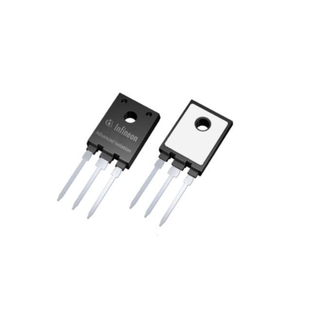
IDFW60C65D1
Emitter�Controlled�Diode�Rapid�1�Advanced�Isolation
Rapid�Switching�Emitter�Controlled�Diode�in�fully�isolated�package
�
Features:
A1 C1 C2 A2
A2
A1
•�650V�Emitter�Controlled�technology
•�Temperature�stable�behaviour�of�key�parameters
•�Low�forward�voltage�(VF)
•�Low�reverse�recovery�charge�(Qrr)
•�Low�reverse�recovery�current�(Irrm)
•�Maximum�junction�temperature�175°C
•�2500�VRMS�electrical�isolation,�50/60�Hz,�t�=�1�min
•�100�%�tested�isolated�mounting�surface
•�Pb-free�lead�plating
•�RoHS�compliant
C
Potential�Applications:
•�Air�Conditioning
•�GPD�(General�Purpose�Drives)
•�Industrial�SMPS
Package�pin�definition:
Fully isolated package TO-247
•�Pin�1�-�anode�(A1)
•�Pin�2�-�cathode�(C)
•�Pin�3�-�anode�(A2)
Product�Validation:
Qualified�for�industrial�applications�according�to�the�relevant�tests
of�JEDEC�47/20/22
Key�Performance�and�Package�Parameters
Type
IDFW60C65D1
Datasheet
www.infineon.com
Vrrm
If
Vf,�Tvj=25°C
Tvjmax
Marking
Package
650V
2x 30A
1.45V
175°C
C60ED1
PG-TO247-3-AI
Please�read�the�Important�Notice�and�Warnings�at�the�end�of�this�document
V�2.2
2019-05-20
�IDFW60C65D1
Emitter�Controlled�Diode�Rapid�1�Advanced�Isolation
Table�of�Contents
Description . . . . . . . . . . . . . . . . . . . . . . . . . . . . . . . . . . . . . . . . . . . . . . . . . . . . . . . . . . . . . . . . . . . . . . . . 1
Table of Contents . . . . . . . . . . . . . . . . . . . . . . . . . . . . . . . . . . . . . . . . . . . . . . . . . . . . . . . . . . . . . . . . . . . 2
Maximum Ratings (per leg) . . . . . . . . . . . . . . . . . . . . . . . . . . . . . . . . . . . . . . . . . . . . . . . . . . . . . . . . . . . . 3
Thermal Resistances (per leg) . . . . . . . . . . . . . . . . . . . . . . . . . . . . . . . . . . . . . . . . . . . . . . . . . . . . . . . . . 3
Electrical Characteristics . . . . . . . . . . . . . . . . . . . . . . . . . . . . . . . . . . . . . . . . . . . . . . . . . . . . . . . . . . . . . . 3
Electrical Characteristics Diagrams . . . . . . . . . . . . . . . . . . . . . . . . . . . . . . . . . . . . . . . . . . . . . . . . . . . . . 6
Package Drawing . . . . . . . . . . . . . . . . . . . . . . . . . . . . . . . . . . . . . . . . . . . . . . . . . . . . . . . . . . . . . . . . . . . 9
Testing Conditions . . . . . . . . . . . . . . . . . . . . . . . . . . . . . . . . . . . . . . . . . . . . . . . . . . . . . . . . . . . . . . . . . 10
Revision History . . . . . . . . . . . . . . . . . . . . . . . . . . . . . . . . . . . . . . . . . . . . . . . . . . . . . . . . . . . . . . . . . . . 11
Disclaimer . . . . . . . . . . . . . . . . . . . . . . . . . . . . . . . . . . . . . . . . . . . . . . . . . . . . . . . . . . . . . . . . . . . . . . . . 12
Datasheet
2
V�2.2
2019-05-20
�IDFW60C65D1
Emitter�Controlled�Diode�Rapid�1�Advanced�Isolation
Maximum�Ratings�(per�leg)
For�optimum�lifetime�and�reliability,�Infineon�recommends�operating�conditions�that�do�not�exceed�80%�of�the�maximum�ratings�stated�in�this�datasheet.
Parameter
Symbol
Value
Unit
Repetitive�peak�reverse�voltage,�Tvj�≥�25°C
VRRM
650
V
Diode�forward�current,�limited�by�Tvjmax
Th�=�25°C
Th�=�65°C
IF
56.0
43.0
A
Diode�pulsed�current,�tp�limited�by�Tvjmax
IFpuls
90.0
A
Diode surge non repetitive forward current
Th�=�25°C,�tp�=�10.0ms,�sine�halfwave
IFSM
Power�dissipation�Th�=�25°C
Power�dissipation�Th�=�65°C
Ptot
100.0
73.0
W
Operating junction temperature
Tvj
-40...+175
°C
Storage temperature
Tstg
-55...+150
°C
A
240.0
Soldering temperature,
wave soldering 1.6mm (0.063in.) from case for 10s
°C
260
Mounting torque, M3 screw
Maximum of mounting processes: 3
M
Isolation�voltage�RMS,�f�=�50/60Hz,�t�=�1min1)
Visol
0.6
Nm
2500
V
Thermal�Resistances�(per�leg)
Parameter
Symbol Conditions
Value
min.
typ.
max.
Unit
Rth�Characteristics
Diode thermal resistance,2)
junction - heatsink
Rth(j-h)
-
1.37
1.50
K/W
Thermal resistance
junction - ambient
Rth(j-a)
-
-
65
K/W
Electrical�Characteristics�(per�leg),�at�Tvj�=�25°C,�unless�otherwise�specified
Parameter
Symbol Conditions
Value
min.
typ.
max.
-
1.45
1.42
1.40
1.75
-
-
1200
40
-
Unit
Static�Characteristic
Diode forward voltage
VF
IF�=�30.0A
Tvj�=�25°C
Tvj�=�125°C
Tvj�=�175°C
Reverse leakage current3)
IR
VR�=�650V
Tvj�=�25°C
Tvj�=�175°C
1)
2)
3)
V
µA
For a proper handling and assembly of the advanced isolation device in the application refer to the note at the package drawing.
At force on body F = 500N, Ta = 25°C
Reverse leakage current per leg specified for operating conditions with zero voltage applied to the other leg.
Datasheet
3
V�2.2
2019-05-20
�IDFW60C65D1
Emitter�Controlled�Diode�Rapid�1�Advanced�Isolation
Electrical�Characteristic,�at�Tvj�=�25°C,�unless�otherwise�specified
Parameter
Symbol Conditions
Value
min.
typ.
max.
-
13.0
-
Unit
Dynamic�Characteristic
Internal emitter inductance
measured 5mm (0.197 in.) from
case
LE
nH
Switching�Characteristics�(per�leg),�Inductive�Load
Parameter
Symbol Conditions
Value
Unit
min.
typ.
max.
Tvj�=�25°C,
VR�=�400V,
IF�=�30.0A,
diF/dt�=�1000A/µs,
Lσ�=�30nH,
Cσ�=�40pF,
switch IGW50N65H5.
-
65
-
ns
-
0.76
-
µC
-
17.6
-
A
-
-1360
-
A/µs
Tvj�=�25°C,
VR�=�400V,
IF�=�30.0A,
diF/dt�=�200A/µs,
Lσ�=�30nH,
Cσ�=�40pF,
switch IGW50N65H5.
-
112
-
ns
-
0.47
-
µC
-
4.5
-
A
-
-655
-
A/µs
Diode�Characteristic,�at�Tvj�=�25°C
Diode reverse recovery time
trr
Diode reverse recovery charge
Qrr
Diode peak reverse recovery current Irrm
Diode peak rate of fall of reverse
recovery�current�during�tb
dirr/dt
Diode reverse recovery time
trr
Diode reverse recovery charge
Qrr
Diode peak reverse recovery current Irrm
Diode peak rate of fall of reverse
recovery�current�during�tb
dirr/dt
Switching�Characteristics�(per�leg),�Inductive�Load
Parameter
Symbol Conditions
Value
Unit
min.
typ.
max.
Tvj�=�175°C,
VR�=�400V,
IF�=�30.0A,
diF/dt�=�1000A/µs,
Lσ�=�30nH,
Cσ�=�40pF,
switch IGW50N65H5.
-
102
-
ns
-
1.80
-
µC
-
25.9
-
A
-
-995
-
A/µs
Tvj�=�125°C,
VR�=�400V,
IF�=�30.0A,
diF/dt�=�200A/µs,
Lσ�=�30nH,
Cσ�=�40pF,
switch IGW50N65H5.
-
148
-
ns
-
0.98
-
µC
-
8.5
-
A
-
-485
-
A/µs
Diode�Characteristic,�at�Tvj�=�175°C/125°C
Diode reverse recovery time
trr
Diode reverse recovery charge
Qrr
Diode peak reverse recovery current Irrm
Diode peak rate of fall of reverse
recovery�current�during�tb
dirr/dt
Diode reverse recovery time
trr
Diode reverse recovery charge
Qrr
Diode peak reverse recovery current Irrm
Diode peak rate of fall of reverse
recovery�current�during�tb
Datasheet
dirr/dt
4
V�2.2
2019-05-20
�IDFW60C65D1
Emitter�Controlled�Diode�Rapid�1�Advanced�Isolation
100
60
90
50
IF,�FORWARD�CURRENT�[A]
Ptot,�POWER�DISSIPATION�[W]
80
70
60
50
40
30
40
30
20
20
10
10
0
25
50
75
100
125
150
0
175
25
Th,�HEATSINK�TEMPERATURE�[°C]
50
75
100
125
150
175
Th,�HEATSINK�TEMPERATURE�[°C]
Figure 1. Power�dissipation�per�leg�as�a�function�of
heatsink�temperature
(Tvj≤175°C)
Figure 2. Diode�forward�current�per�leg�as�a�function�of
heatsink�temperature
(Tvj≤175°C)
200
0.1
D = 0.5
0.2
0.1
0.05
0.01
0.02
0.01
single pulse
0.001
160
140
120
100
80
60
40
1E-4
20
i:
1
2
3
4
5
6
7
ri[K/W]: 0.202274 0.337235 0.289542 0.199229 0.422136 0.046667 9.6E-3
τi[s]:
2.4E-4
1.4E-3
8.6E-3
0.071422 0.525208 3.996801 20.96846
1E-5
1E-7
Tvj�=�25°C,�IF�=�30A
Tvj�=�125°C,�IF�=�30A
Tvj�=�175°C,�IF�=�30A
180
trr,�REVERSE�RECOVERY�TIME�[ns]
Zth(j-c),�TRANSIENT�THERMAL�IMPEDANCE�[K/W]
1
1E-6
1E-5
1E-4
0.001
0.01
0.1
0
200
1
tp,�PULSE�WIDTH�[s]
400
600
800
1000
1200
1400
dIF/dt,�DIODE�CURRENT�SLOPE�[A/µs]
Figure 3. Diode�transient�thermal�impedance�per�leg�as Figure 4. Typical�reverse�recovery�time�per�leg�as�a
a�function�of�pulse�width
function�of�diode�current�slope
(D=tp/T)
(VR=400V)
Datasheet
5
V�2.2
2019-05-20
�IDFW60C65D1
Emitter�Controlled�Diode�Rapid�1�Advanced�Isolation
2.50
30
Irrm,��REVERSE�RECOVERY�CURRENT�[A]
Qrr,�REVERSE�RECOVERY�CHARGE�[µC]
2.25
35
Tvj�=�25°C,�IF�=�30A
Tvj�=�125°C,�IF�=�30A
Tvj�=�175°C,�IF�=�30A
2.00
1.75
1.50
1.25
1.00
0.75
0.50
Tvj�=�25°C,�IF�=�30A
Tvj�=�125°C,�IF�=�30A
Tvj�=�175°C,�IF�=�30A
25
20
15
10
5
0.25
0.00
200
400
600
800
1000
1200
0
200
1400
dIF/dt,�DIODE�CURRENT�SLOPE�[A/µs]
Figure 5. Typical�reverse�recovery�charge�per�leg�as�a
function�of�diode�current�slope
(VR=400V)
800
1000
1200
1400
60
Tvj�=�25°C,�IF�=�30A
Tvj�=�125°C,�IF�=�30A
Tvj�=�175°C,�IF�=�30A
Tvj�=�25°C
Tvj�=�175°C
50
-400
IF,�FORWARD�CURRENT�[A]
dIrr/dt,�DIODE�PEAK�RATE�OF�FALL�OF�Irr�[A/µs]
600
Figure 6. Typical�peak�reverse�recovery�current�per�leg
as�a�function�of�diode�current�slope
(VR=400V)
0
-200
400
dIF/dt,�DIODE�CURRENT�SLOPE�[A/µs]
-600
-800
-1000
-1200
-1400
40
30
20
-1600
10
-1800
-2000
200
400
600
800
1000
1200
0
0.00
1400
dIF/dt,�DIODE�CURRENT�SLOPE�[A/µs]
Figure 7. Typical�diode�peak�rate�of�fall�of�rev.�rec.
current�per�leg�as�a�function�of�diode�current
slope
(VR=400V)
Datasheet
0.25
0.50
0.75
1.00
1.25
1.50
1.75
2.00
VF,�FORWARD�VOLTAGE�[V]
Figure 8. Typical�diode�forward�current�per�leg�as�a
function�of�forward�voltage
6
V�2.2
2019-05-20
�IDFW60C65D1
Emitter�Controlled�Diode�Rapid�1�Advanced�Isolation
2.25
IF�=�7.5A
IF�=�15A
IF�=�30A
IF�=�45A
IF�=�60A
VF,�FORWARD�VOLTAGE�[V]
2.00
1.75
1.50
1.25
1.00
0.75
0.50
25
50
75
100
125
150
175
Tvj,�JUNCTION�TEMPERATURE�[°C]
Figure 9. Typical�diode�forward�voltage�per�leg�as�a
function�of�junction�temperature
Datasheet
7
V�2.2
2019-05-20
�IDFW60C65D1
Emitter�Controlled�Diode�Rapid�1�Advanced�Isolation
PG-TO247-3-AI (PGHSIP2473)
DIMENSIONS
A
A1
A2
A3
b
c
D
D1
E
E1
e
L
L1
øP
øP1
Q
Note:
Datasheet
MILLIMETERS
MAX.
5.18
4.90
2.59
0.28
1.30
0.70
22.40
17.16
15.90
13.88
5.44
18.31
18.91
2.76
2.96
3.50
3.70
5.70
5.90
5.96
6.36
MIN.
4.70
2.23
0.20
1.10
0.50
22.20
16.96
15.70
13.68
DOCUMENT NO.
Z8B00186434
REVISION
02
SCALE 3:1
0 1 2 3 4 5 6 7 8mm
EUROPEAN PROJECTION
ISSUE DATE
05.06.2018
For a proper handling and assembly of the advanced isolation device in the application the isolation layer must not be exposed to potential
penetration via sharp implements or mechanical impacts/shocks, which exceed levels indicated in International Standard (IEC6006826 and
IEC60068227). The advanced isolation device is intended only to be used assembled on an appropriate heatsink with recommended flatness
of