IDWD20G120C5
IGC13R65U8W2 IGC13R65U8W2
IGC13R65U8W2
IGC13R65U8W2
5 th Generation CoolSiC TM
IGC13R65U8W2
SiC Diode
1200V Schottky Diode
Features
No reverse recovery current / no forward recovery
High surge current capability
Temperature independent switching behaviour
Low forward voltage even at high operating temperature
Tight forward voltage distribution
1
Specified dv/dt ruggedness
Pb-free lead plating; RoHS compliant
2
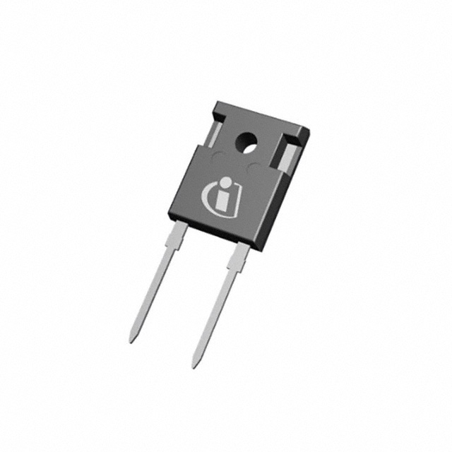
Pin definition
Potential applications
Pin 1 and backside: Cathode 1
Industrial power supplies: Industrial UPS
Pin 2: Anode
Infrastructure-Charge: Charger
Metal treatment: Welding
Solar central inverters, Solar string inverter and Solar optimizer
CASE
2
Product validation
Qualified for industrial applications according to the relevant tests of JEDEC 47/20/22
Description
System efficiency improvement over Si diodes
Enabling higher frequency / increased power density solutions
System size/cost savings due to reduced heatsink requirements and smaller magnetics
Reduced EMI
Highest efficiency across the entire load range
Robust diode operation during surge events
High reliability
Related Links: www.infineon.com/SiC
Key performance parameters
Type
IDWD20G120C5
VDC
IF
QC
Tvj,max
Marking
Package
1200 V
20 A
106nC
175°C
D2012C5
PG-TO247-2
Datasheet
www.infineon.com
Please read the Important Notice and Warnings at the end of this document
page 1 of 12
V 2.1
2021-03-01
�5th Generation CoolSiCTM 1200V Schottky Diode
SiC Diode
Table of contents
Table of contents
Features ........................................................................................................................................ 1
Potential applications ..................................................................................................................... 1
Product validation .......................................................................................................................... 1
Description .................................................................................................................................... 1
Key performance parameters........................................................................................................... 1
Table of contents ............................................................................................................................ 2
1
Maximum ratings ................................................................................................................... 3
2
Thermal resistances ............................................................................................................... 5
3
Electrical Characteristics ........................................................................................................ 6
4
Electrical Characteristics Diagrams .......................................................................................... 7
5
Package Drawing .................................................................................................................. 10
Revision history............................................................................................................................. 11
Datasheet
www.infineon.com
Please read the Important Notice and Warnings at the end of this document
page 2 of 12
V 2.1
2021-03-01
�5th Generation CoolSiCTM 1200V Schottky Diode
SiC Diode
Maximum ratings
1
Maximum ratings
Note:
For optimum lifetime and reliability, Infineon recommends operating conditions that do not
exceed 80% of the maximum ratings stated in this datasheet.
Parameter
Repetitive peak reverse voltage
TC ≥ 25°C
Symbol
Value
VRRM
1200
Unit
V
Continuous forward current for Rth(j-c,max)
TC = 156°C, D=1
IF
TC = 135°C, D=1
TC = 25°C, D=1
20
29
A
62
Surge repetitive forward current, sine halfwave1
TC=25°C, tp=10ms
IF,RM
TC=100°C, tp=10ms
80
60
A
Surge non-repetitive forward current, sine halfwave
TC=25°C, tp=10ms
IF,SM
TC=150°C, tp=10ms
190
A
180
Non-repetitive peak forward current
TC = 25°C, tp=10 µs
IF,max
1774
A
∫ i²dt
180
A²s
i²t value
TC = 25°C, tp=10 ms
TC = 150°C, tp=10 ms
162
Diode dv/dt ruggedness
VR=0...960 V
Power dissipation for Rth(j-c,max)
TC = 25°C
1
dv/dt
150
V/ns
Ptot
250
W
Not subject to production test. The test was performed with 20000 pulses (two consecutive half-wave rectified sines with 10 ms period).
Datasheet
www.infineon.com
Please read the Important Notice and Warnings at the end of this document
page 3 of 12
V 2.1
2021-03-01
�5th Generation CoolSiCTM 1200V Schottky Diode
SiC Diode
Maximum ratings
Operating temperature
Tvj
-55…175
°C
Storage temperature
Tstg
-55…150
°C
Tsold
260
°C
M
0.6
Nm
Soldering temperature,
wave soldering only allowed at leads
1.6mm (0.063 in.) from case for 10 s
Mounting torque, M3 screw
Maximum of mounting processes: 3
Datasheet
www.infineon.com
Please read the Important Notice and Warnings at the end of this document
page 4 of 12
V 2.1
2021-03-01
�5th Generation CoolSiCTM 1200V Schottky Diode
SiC Diode
Thermal resistances
2
Thermal resistances
Value
Parameter
Symbol
Conditions
Unit
min.
typ.
max.
-
0.45
0.6
K/W
-
-
62
K/W
Characteristic
Diode thermal resistance,
junction – case
Thermal resistance,
junction – ambient
Datasheet
www.infineon.com
Rth(j-c)
Rth(j-a)
leaded
Please read the Important Notice and Warnings at the end of this document
page 5 of 12
V 2.1
2021-03-01
�5th Generation CoolSiCTM 1200V Schottky Diode
SiC Diode
Electrical Characteristics
3
Electrical Characteristics
Static Characteristics, at Tvj=25°C, unless otherwise specified
Parameter
Symbol Conditions
DC blocking voltage
VDC
Diode forward voltage
VF
Reverse current
IR
min.
Value
typ.
max.
Tvj= 25°C, IR=500µA
1200
-
-
IF= 20A, Tvj=25°C
IF= 20A, Tvj=150°C
VR=1200V, Tvj=25°C
VR=1200V, Tvj=150°C
-
1.4
1.7
12
58
1.65
166
-
Value
typ.
max.
Unit
V
V
µA
Dynamic Characteristics, at Tvj=25°C, unless otherwise specified
Parameter
Symbol Conditions
Total capacitive charge
min.
Unit
VR = 800V, Tvj=150°C & 25°C
QC
VR
QC C (V )dV
-
106
-
nC
-
1368
96
76
-
pF
0
Total Capacitance
Datasheet
www.infineon.com
C
VR=1 V, f=1 MHz
VR=400 V, f=1 MHz
VR=800 V, f=1 MHz
Please read the Important Notice and Warnings at the end of this document
page 6 of 12
V 2.1
2021-03-01
�5th Generation CoolSiCTM 1200V Schottky Diode
SiC Diode
Electrical Characteristics Diagrams
4
Electrical Characteristics Diagrams
250
300
D= 0.10
D= 0.30
250
200
D= 0.50
D= 0.70
D= 1.00
200
IF [A]
150
P [W]
150
100
100
50
50
0
0
25
50
75
100
125
150
25
175
50
75
Tc [°C]
Figure 1. Power dissipation as function of
case temperature, Ptot=f(TC), Rth(j-c),max
100 125
Tc [°C]
150
175
Figure 2. Diode forward current as function
of temperature, parameter: Tvj≤175°C, Rth(jc),max, D=duty cycle, Vth, Rdiff @ Tvj=175°C
200
40
-55 C
180
35
-55 C
160
30
25 C
25 C
140
100 C
120
IF [A]
IF [A]
25
150 C
20
100 C
100
80
15
175 C
60
10
150 C
40
5
175 C
20
0
0
0
0.5
1
VF [V]
1.5
2
2.5
Figure 3. Typical forward characteristics,
IF=f(VF), tp= 10 µs, parameter: Tvj
Datasheet
www.infineon.com
0
1
2
3
VF [V]
4
5
6
Figure 4. Typical forward characteristics in
surge current, IF=f(VF), tp= 10 µs, parameter: Tvj
Please read the Important Notice and Warnings at the end of this document
page 7 of 12
V 2.1
2021-03-01
�5th Generation CoolSiCTM 1200V Schottky Diode
SiC Diode
Electrical Characteristics Diagrams
120
1E-4
100
1E-5
80
IR [A]
QC [nC]
1E-6
60
175 C
150 C
1E-7
40
100 C
1E-8
20
25 C
-55 C
0
1E-9
100
400
700
dIF/dt [A/µs]
1000
Figure 5. Typical capacitive charge as
function of current slope2, QC=f(dIF/dt),
Tvj=150°C
200
400
600
800
VR [V]
1000
1200
Figure 6. Typical reverse characteristics,
IR=f(VR), parameter: Tvj
2) guaranteed by design
1800
1600
1
1200
1000
C [pF]
Zthjc [K/W]
1400
D= 0.50
D= 0.20
0.1
800
600
D= 0.10
D= 0.05
400
D= 0.02
200
D= 0.01
Single Pulse
0.01
1E-6
1E-5
1E-4
1E-3
tp [s]
1E-2
1E-1
www.infineon.com
0
1E0
Figure 7. Max. transient thermal impedance,
Zth,j-c=f(tP), parameter: D=tP/T
Datasheet
0
1
10
100
1000
VR [V]
Figure 8. Typical capacitance as function of
reverse voltage, C=f(VR); Tvj=25°C; f=1 MHz
Please read the Important Notice and Warnings at the end of this document
page 8 of 12
V 2.1
2021-03-01
�5th Generation CoolSiCTM 1200V Schottky Diode
SiC Diode
Electrical Characteristics Diagrams
70
60
EC [µJ]
50
40
30
20
10
0
0
200
400
600 800
VR [V]
1000 1200
Figure 9. Typical capacitively stored energy
as function of reverse voltage, EC=f(VR)
Datasheet
www.infineon.com
Please read the Important Notice and Warnings at the end of this document
page 9 of 12
V 2.1
2021-03-01
�5th Generation CoolSiCTM 1200V Schottky Diode
SiC Diode
Package Drawing
5
Package Drawing
Datasheet
www.infineon.com
Please read the Important Notice and Warnings at the end of this document
page 10 of 12
V 2.1
2021-03-01
�5th Generation CoolSiCTM 1200V Schottky Diode
SiC-Diode
Revision history
Revision history
Document
version
Date of release
Description of changes
V 1.0
2018-12-21
Preliminary Datasheet
V 2.0
2019-01-30
Final Datasheet
V 2.1
2021-03-01
Increased dv/dt ruggedness
Datasheet
www.infineon.com
Please read the Important Notice and Warnings at the end of this document
page 11 of 12
V 2.1
2021-03-01
�Trademarks
All referenced product or service names and trademarks are the property of their respective owners.
Edition 2021-03-01
Published by
Infineon Technologies AG
81726 München, Germany
© 2021 Infineon Technologies AG.
All Rights Reserved.
Do you have a question about this
document?
Email: erratum@infineon.com
Document reference
n.a.
IMPORTANT NOTICE
The information given in this document shall in no
event be regarded as a guarantee of conditions or
characteristics (“Beschaffenheitsgarantie”) .
With respect to any examples, hints or any typical
values stated herein and/or any information
regarding the application of the product, Infineon
Technologies hereby disclaims any and all
warranties and liabilities of any kind, including
without limitation warranties of non-infringement
of intellectual property rights of any third party.
In addition, any information given in this document
is subject to customer’s compliance with its
obligations stated in this document and any
applicable legal requirements, norms and
standards concerning customer’s products and any
use of the product of Infineon Technologies in
customer’s applications.
The data contained in this document is exclusively
intended for technically trained staff. It is the
responsibility of customer’s technical departments
to evaluate the suitability of the product for the
intended application and the completeness of the
product information given in this document with
respect to such application.
For further information on the product, technology,
delivery terms and conditions and prices please
contact your nearest Infineon Technologies office
(www.infineon.com).
Please note that this product is not qualified
according to the AEC Q100 or AEC Q101 documents
of the Automotive Electronics Council.
WARNINGS
Due to technical requirements products may
contain dangerous substances. For information on
the types in question please contact your nearest
Infineon Technologies office.
Except as otherwise explicitly approved by Infineon
Technologies in a written document signed by
authorized
representatives
of
Infineon
Technologies, Infineon Technologies’ products may
not be used in any applications where a failure of
the product or any consequences of the use thereof
can reasonably be expected to result in personal
injury.
�