IFX21004TN V51
Dual Voltage Regulator with 5 V and 15 V Outputs
IFX21004TN V51
Data Sheet
Rev. 1.00, 2010-11-04
Standard Power
�Dual Voltage Regulator with 5 V and 15 V Outputs
1
IFX21004TN V51
Overview
Features
•
•
•
•
•
•
•
•
Dual Output: 5 V and 15 V
High Input Voltage Range: up to 60 V Peak
High Output Current Capability 100 mA and 30 mA
High Output Voltage Accuracy
Very low Current Consumption
Overtemperature Shutdown
Thermal Optimized Package
Green Product (RoHS compliant)
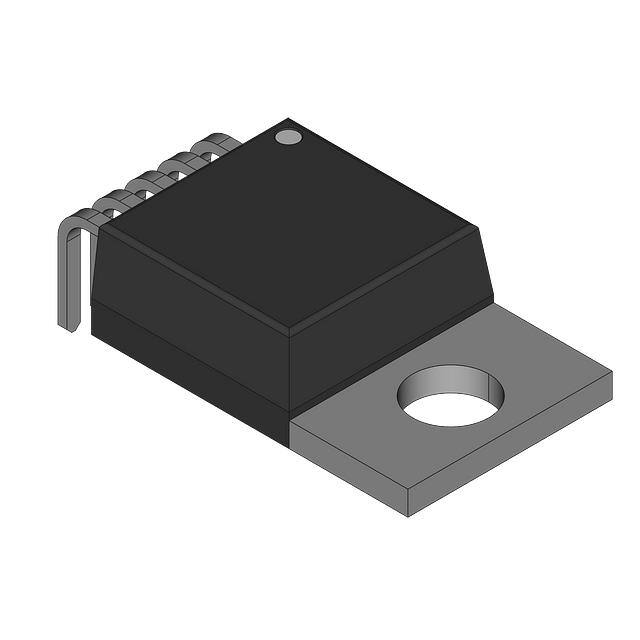
PG-TO220-5
For automotive applications please refer to the Infineon TLE- and TLF-series voltage regulators.
Description
The IFX21004TN V51 is a monolithic integrated voltage regulator providing two output voltages: Output Q1 is a 5
V output for loads up to 100 mA and output Q2 is a 15 V output providing up to 30 mA. The device is available in
the PG-TO220-5 package.
The IFX21004TN V51 is designed to supply any system that requires 5 V and 15 V. These can be for example
systems with a microcontroller (5 V) and a standard MOS-driver-IC (15 V). To fulfill also the requirements of
severe operating conditions the IFX21004TN V51 is able to operate across a wide junction temperature range of
-40 °C < Tj < 150 °C and is also equipped with additional protection functions.
Both outputs are protected against overload by an integrated output current limitation circuit. The built-in
overtemperature shutdown circuit protects the device against overheat.
The IC operates across a wide input voltage range from 20 V up to 60 V peak and up to 40V for continuous
operation. The output voltages are regulated to VQ1 = 5 V and VQ2 = 15 V. The standard PG-TO220-5 package is
especially suitable for this kind of application, as it reduces system cost and provides excellent thermal
characteristics.
Type
Package
Marking
IFX21004TN V51
PG-TO220-5
IFX21004
Data Sheet
2
Rev. 1.00, 2010-11-04
�IFX21004TN V51
Block Diagram
2
Block Diagram
I
+
TSD
Bias
&
BG
TSD: Overtemperature
Shutdown
BG:
Protect.
Q1
+
-
Protect.
Bandgap Reference
Q2
n.c.
Figure 1
Data Sheet
GND
Block Diagram
3
Rev. 1.00, 2010-11-04
�IFX21004TN V51
Pin Configuration
3
Pin Configuration
3.1
Pin Assignment
GND
1
5
I
GND Q2
n.c. Q1
PG-TO220-5-12.vsd
Figure 2
Pin Configuration
3.2
Pin Definitions and Functions
Pin
Symbol
Function
1
I
Input voltage
block to ground directly at the IC with a ceramic capacitor.
2
n.c.
not connected
leave open, don’t connect
3
GND
Ground
connect to tab (heat sink)
4
Q1
5V-Output voltage, e.g. for microcontroller and logic circuit
block to ground with a capacitor respecting the values given in “Output Capacitor’s
Requirements for Stability” on Page 7
5
Q2
15V-Output voltage, e.g. for MOS driver circuit
block to ground with a capacitor as specified in “Output Capacitor’s
Requirements for Stability” on Page 8
Tab
–
Tab
connect to pin3 (GND) and heatsink area
Data Sheet
4
Rev. 1.00, 2010-11-04
�IFX21004TN V51
General Product Characteristics
4
General Product Characteristics
4.1
Absolute Maximum Ratings
Table 1
Absolute Maximum Ratings
Tj = -40 °C to +150 °C; all voltages with respect to ground, positive current flowing into pin (unless otherwise
specified)
Parameter
Symbol
Limit Values
Unit
Remarks
during max. 400ms
see also Chapter 6
Min.
Max.
-0.3
60
V
-0.3
40
V
VQ1
VQ2
-0.3
6.5
V
–
-0.3
20
V
–
Tj
Tstg
-40
150
°C
–
-50
150
°C
–
VESD
VESD
-2
2
kV
HBM1)
-1
1
kV
CDM2)
Input
VI
Voltage
Outputs Q1, Q2
Voltage
Voltage
Temperatures
Junction Temperature
Storage Temperature
ESD-Protection
All Pins
All Pins
1) ESD susceptibility, HBM according to EIA/JESD 22-A114B
2) ESD susceptibility, Charged Device Model “CDM” EIA/JESD22-C101 or ESDA STM5.3.1
Note: Stresses above the ones listed here may cause permanent damage to the device. Exposure to absolute
maximum rating conditions for extended periods may affect device reliability.
Note: Integrated protection functions are designed to prevent IC destruction under fault conditions described in the
data sheet. Fault conditions are considered as “outside” normal operating range. Protection functions are
not designed for continuous repetitive operation.
4.2
Operating Range
Table 2
Operating Range
Parameter
Symbol
Limit Values
Min.
Max.
Unit
Remarks
Input Voltage Range for Q1
VI1
12
60
V
only Q1 functional;
during max. 400ms1)
12
40
V
only Q1 functional1)
Input Voltage Range for Q2
VI1
VI2
20
60
V
Q1 and Q2 functional;
during max. 400ms1)
20
40
V
Q1 and Q2 functional1)
Junction temperature
VI2
Tj
-40
150
°C
–
1) also consider the specification of the Dropout Voltage VDRQ1, VDRQ2 given in the Table 4
Data Sheet
5
Rev. 1.00, 2010-11-04
�IFX21004TN V51
General Product Characteristics
4.3
Thermal Resistances
Table 3
Thermal Resistances1)
Parameter
Symbol
Typ. Limit
Value
Unit
Remarks
Junction to Case
RthJC
4.1
K/W
underlying P = 2W power
dissipation with power zener
activated2)
Junction to Case
RthJC
6.1
K/W
underlying P = 2W power
dissipation with power zener
deactivated3)
1) not subject to production test, specified by design
2) for the taken case with the zener diode activated the power distribution on the chip is given as follows. Power zener:
PZener = 0.85W; power stage Q1: PPowerstageQ1 = 1.03W; power stage Q2: PPowerstageQ2 = 0.12W
3) for the taken case with the zener diode deactivated the power distribution on the chip is given as follows. Power stage Q1
PPowerstageQ1 = 1.72W; power stage Q2 PPowerstageQ2 = 0.28W
Note: In the operating range, the functions given in the circuit description are fulfilled.
Data Sheet
6
Rev. 1.00, 2010-11-04
�IFX21004TN V51
Electrical Characteristics
5
Electrical Characteristics
Table 4
Electrical Characteristics
VI = 24 V; -40 °C < Tj < 150 °C; all voltages with respect to ground; positive current defined flowing out of pin;
unless otherwise specified.
Parameter
Symbol
Limit Values
Min.
Typ.
Max.
Unit
Test Condition
IQ1 = 1 mA;
IQ2 = 1 mA
IQ1 = 100 mA;
IQ2 = 30 mA
Current Consumption
Quiescent Current
Iq = II - (IQ1 + IQ2)
Iq
–
700
1000
μA
Current Consumption
Iq = II - (IQ1 + IQ2)
Iq
–
1
3.5
mA
Output Voltage
VQ1
4.85
5.00
5.15
V
Output Voltage
VQ1
IQ1
VDRQ1
4.75
–
5.25
V
101
180
600
mA
–
5
10
V
Load Regulation
(steady state)
ΔVQ1
–
20
50
mV
Line Regulation
(steady state)
ΔVQ1
–
15
50
mV
Power Supply Ripple
Rejection2)
PSRRQ1
–
55
–
dB
Output Capacitor’s
Requirements for Stability
CQ1
ESR(CQ1)
1.0
–
–
μF
–2)3)
–
–
5.0
Ω
–2)
Output Q1 (5 V)
Output Current Limitation
Dropout Voltage
VDRQ1 = VI - VQ1
Data Sheet
7
IQ1 = 80 mA;
Tj = 25 °C
1 mA < IQ1 < 100 mA
VQ1,nom - 100mV; VI =24V
IQ1 = 100 mA;
IQ2 = 30 mA1)
1 mA < IQ1 < 100 mA;
VI = 24 V
IQ1 = 1 mA;
24 V < VI < 40 V
fr =100 Hz;
Vr = 1Vpp
Rev. 1.00, 2010-11-04
�IFX21004TN V51
Electrical Characteristics
Table 4
Electrical Characteristics (cont’d)
VI = 24 V; -40 °C < Tj < 150 °C; all voltages with respect to ground; positive current defined flowing out of pin;
unless otherwise specified.
Parameter
Symbol
Limit Values
Min.
Typ.
Max.
Unit
Test Condition
IQ2 = 15 mA;
Tj = 25 °C
1 mA < IQ2 < 30 mA
VQ2,nom - 100mV; VI =24V
IQ2 = 30 mA;
IQ1 = 100 mA1)
1 mA < IQ2 < 30 mA;
VI = 24 V
IQ2 = 1 mA;
24 V < VI < 40 V
fr =100 Hz;
Vr = 1Vpp
Output Q2 (15 V)
Output Voltage
VQ2
14.4
15.0
15.6
V
Output Voltage
VQ2
IQ2
VDRQ2
14.25
–
15.75
V
31
100
220
mA
–
3
6
V
Load Regulation
ΔVQ2
–
50
150
mV
Line Regulation
ΔVQ2
–
30
150
mV
Power Supply Ripple
Rejection2)
PSRRQ2
–
50
–
dB
Output Capacitor’s
Requirements for Stability
CQ2
ESR(CQ2)
1.0
–
–
μF
–2)3)
–
–
5.0
Ω
–2)
Output Current Limitation
Dropout Voltage
VDRQ2 = VI - VQ2
1) Drop voltage = VI - VQ (measured when the output voltage has dropped 100 mV from the nominal value).
2) not subject to production test, specified by design.
3) for further details please refer to Chapter 6.
Note: The listed characteristics are ensured over the operating range of the integrated circuit. Typical
characteristics specified mean values expected over the production spread. If not otherwise specified,
typical characteristics apply at TA = 25 °C and the given supply voltage.
Data Sheet
8
Rev. 1.00, 2010-11-04
�IFX21004TN V51
Electrical Characteristics
5.1
Typical Performance Characteristics
Output Voltage VQ1 versus
Junction Temperature Tj
Output Voltage VQ2 versus
Junction Temperature Tj
5,20
5,15
5,10
15,10
5,05
15,05
5,00
15,00
4,95
14,95
4,90
14,90
4,85
14,85
4,80
14,80
-40
-40
0
40
80
VI = 24 V
IQ = 1 mA
15,15
VQ2 [mV]
VQ1 [mV]
15,20
VI = 24 V
IQ = 1 mA
120
0
Output Current Limitation Q1 versus
Junction Temperature Tj (@ VQ1,nom - 100mV)
120
Output Current Limitation Q2 versus
Junction Temperature Tj (@ VQ2,nom - 100mV)
100,00
VI = 24 V
VI = 24 V
VQ2 = V Q2,nom- 100mV
VQ1 = V Q1,nom‐ 100mV
90,00
190,00
80,00
180,00
I Q2 [mA]
I Q1 [mA]
80
Tj [° C]
Tj [° C]
200,00
40
170,00
70,00
60,00
160,00
50,00
150,00
40,00
140,00
-40
30,00
-40
0
40
80
120
40
80
120
Tj [° C]
Tj [° C]
Data Sheet
0
9
Rev. 1.00, 2010-11-04
�IFX21004TN V51
Electrical Characteristics
Line Regulation ΔVQ1,line versus
Input Voltage Change VI
Line Regulation ΔVQ2,line versus
Input Voltage Change VI
30
20
15
20
10
5
Δ VQ2 [mV]
Δ VQ1 [mV]
10
0
-5
0
-10
-10
Tj = - 40 C
-15
Tj = - 40 C
-20
Tj = 25 C
Tj = 25 C
Tj = 150 C
-20
24
Tj = 150 C
-30
29
34
39
24
29
34
VI [V]
VI [V]
Load Regulation ΔVQ1,load versus
Output Current Change IQ
Load Regulation ΔVQ2,load versus
Output Current Change IQ
0
0
VI = 20 V
VI = 20 V
-4
-10
Δ VQ2 [mV]
Δ VQ1 [mV]
39
-8
-12
-30
Tj = - 40 C
-16
-20
Tj = - 40 C
Tj = 25 C
Tj = 25 C
Tj = 150 C
Tj = 150 C
-40
-20
0
20
40
60
80
0
100
20
30
IQ [mA]
IQ [mA]
Data Sheet
10
10
Rev. 1.00, 2010-11-04
�IFX21004TN V51
Application Information
6
Application Information
Note: The following information is given as a hint for the implementation of the device only and shall not be
regarded as a description or warranty of a certain functionality, condition or quality of the device.
I
Batt.
20 V
:
40 V
60 V peak
IFX21004
100 nF
Q1
5V
Q2
n.c. GND
15 V
+
22 µF + 22 µF
25 V
25 V
GND
Figure 3
Application Circuit
Note: This is a very simplified example of an application circuit. The function must be verified in the real application.
The IFX21004TN V51 is operating from 20 V < VI < 40 V (60 V Peak) and can be directly connected to e.g. a
battery line. The maximum output current of this regulator is controlled and limited internally; its output short circuit
protection to ground is ensured up to VI-values of up to 24V.
When any high frequency disturbance is existing and should be filtered, an input capacitor in the range of 100 nF
is helpful.
At both outputs Q1 and Q2 capacitors CQ1 and CQ2 are required in any case to maintain regulating stability.
Therefore as minimum values the specification in Table 4 “Electrical Characteristics” on Page 7 needs to be
respected. In addition, to keep a good line transient regulation1) and load transient regulation2), capacitor values
of CQ1 = CQ2 > 22 µF are recommended.
The IFX21004TN V51 is capable to withstand input voltages exceeding its nominal operating range up to values
of 60 V during short time periods of up to 400ms. Such short input voltage pulses exceeding 40 V are absorbed
by activating an internal zener diode structure. Please note in this context that, due to hysteresis, in some cases
the zener diode may remain activated also after the pulse when the input voltage is afterwards around values of
40V. If in such cases the input voltage is lowered afterwards the power zener will be switched off again. During
the switching of the zener diode the effects of potential switching noise needs to be considered as they may cause
transients on the outputs Q1 and Q2. The occurrence of such transient output voltages is dependent on the
application’s load as well as the used output capacitors. Such potential output transients can be minimized by
using larger values for CQ1 and CQ2 that will damp such output transients.
1) fast voltage transients at the regulator’s input
2) fast current transients at the regulator’s output
Data Sheet
11
Rev. 1.00, 2010-11-04
�IFX21004TN V51
Package Outlines
Package Outlines
10 ±0.2
A
9.9 ±0.2
B
1)
1.27 ±0.1
2.8 ±0.2
C
0.05
2.4
13 ±0.5
0...0.3
4.4
11 ±0.5
1)
12.95
15.65 ±0.3
17 ±0.3
8.5
3.7 -0.15
0.5 ±0.1
0...0.15
2.4
5 x 0.8 ±0.1
4 x 1.7
1)
Figure 4
9.25 ±0.2
7
0.25
M
A B C
Typical
Metal surface min. X = 7.25, Y = 12.3
All metal surfaces tin plated, except area of cut.
PG-TO220-5 (Plastic Small Outline Transistor)
Green Product (RoHS compliant)
To meet the world-wide customer requirements for environmentally friendly products and to be compliant with
government regulations the device is available as a green product. Green products are RoHS-Compliant (i.e
Pb-free finish on leads and suitable for Pb-free soldering according to IPC/JEDEC J-STD-020).
For further information on alternative packages, please visit our website:
http://www.infineon.com/packages.
Data Sheet
12
Dimensions in mm
Rev. 1.00, 2010-11-04
�IFX21004TN V51
Revision History
8
Revision History
Revision
Date
Changes
1.00
2010-11-04
Data Sheet Initial Release
Data Sheet
13
Rev. 1.00, 2010-11-04
�Edition 2010-11-04
Published by
Infineon Technologies AG
81726 Munich, Germany
© 2010 Infineon Technologies AG
All Rights Reserved.
Legal Disclaimer
The information given in this document shall in no event be regarded as a guarantee of conditions or
characteristics. With respect to any examples or hints given herein, any typical values stated herein and/or any
information regarding the application of the device, Infineon Technologies hereby disclaims any and all warranties
and liabilities of any kind, including without limitation, warranties of non-infringement of intellectual property rights
of any third party.
Information
For further information on technology, delivery terms and conditions and prices, please contact the nearest
Infineon Technologies Office (www.infineon.com).
Warnings
Due to technical requirements, components may contain dangerous substances. For information on the types in
question, please contact the nearest Infineon Technologies Office.
The Infineon Technologies component described in this Data Sheet may be used in life-support devices or systems
and/or automotive, aviation and aerospace applications or systems only with the express written approval of
Infineon Technologies, if a failure of such components can reasonably be expected to cause the failure of that lifesupport automotive, aviation and aerospace device or system or to affect the safety or effectiveness of that device
or system. Life support devices or systems are intended to be implanted in the human body or to support and/or
maintain and sustain and/or protect human life. If they fail, it is reasonable to assume that the health of the user
or other persons may be endangered.
�