IFX54211MB V33
High PSRR Low Dropout Linear Voltage Regulator
Data Sheet
Rev. 1.0, 2015-08-26
Standard Power
�High PSRR Low Dropout Linear Voltage Regulator
1
IFX54211MB V33
Overview
Features
•
•
•
•
•
•
•
•
•
•
•
•
•
•
Output Voltage: 3.3 V
Output Voltage Accuracy of ±3 %
Output Currents up to 150 mA
Extended Input Voltage Operating Range of 2.7 V to 18 V
Enable Functionality
Low Dropout Voltage: typ. 290mV
Very Low Quiescent Current: typ. 50 µA
Very Low Shutdown Current: typ. 0.01 µA
Very High PSRR: typ. 63dB at 10 kHz
Output Current Limitation
Short Circuit protected
Overtemperature Shutdown
Wide Temperature Range From -40 °C up to 125 °C
Green Product (RoHS compliant)
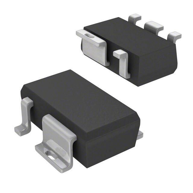
PG-SCT595
Functional Description
The IFX54211MB V33 is a monolithic integrated fixed linear voltage regulator for load currents up to 150 mA. The
IC regulates an input voltage VIN up to 18 V to a fixed output voltage of 3.3 V with a precision of ±3 %. The
IFX54211MB V33 is especially designed for applications requiring very low standby currents, e.g. with a
permanent connection to a power supply, e.g. like a preregulating DCDC converter. Besides the very low
quiescent current the current consumption of the device remains low also for higher load currents thanks to its
PMOS powerstage. The IFX54211MB V33 combines in an ideal way a 150 mA current capability with extremely
small package outlines, low dropout capability and high Power Supply Ripple Rejection PSRR over a wide
frequency range. The component can be enabled/disabled via the Enable input. The device is available in a very
small surface mounted PG-SCT595 package and is designed for the harsh environment of industrial applications.
Therefore it is protected against overload, short circuit and overtemperature conditions by the implemented output
current limitation and the overtemperature shutdown circuit. The IFX54211MB V33 can be also used in all other
applications requiring a stabilized 3.3 V voltage.
Choosing External Components
The input capacitor CIN is recommended for compensating line influences. An output capacitor COUT is necessary
for the stability of the regulating circuit. One strength of the device is that stability is guaranteed already for very
Type
Package
Marking
IFX54211MB V33
PG-SCT595
51
Data Sheet
2
Rev. 1.0, 2015-08-26
�IFX54211MB V33
Overview
small output capacitors down to just 1 µF and at the same time for a wide ESR range from ≤ 10 Ω down to ceramic
values within the whole operating temperature range and thus allowing the user a maximized flexibility in the
choice of an output capacitor COUT. For details please refer to “Functional Range” on Page 7.
The qualification of this product is based on JEDEC JESD47 and may reference existing qualification results of
similar products. Such referring is justified by the structural similarity of the products. The product is not qualified
and manufactured according to the requirements of Infineon Technologies with regard to automotive and/or
transportation applications. Infineon Technologies administrates a comprehensive qualify management system
according to the latest version of the ISO9001 and ISO/TS 16949
The most updated certificates of the aforesaid ISO9001 and ISOTS 16949 are available on the Infineon
Technologies webpage http://www.infineon.com/cms/en/product/technology/quality/
Data Sheet
3
Rev. 1.0, 2015-08-26
�IFX54211MB V33
Block Diagram
2
Block Diagram
OUT
IN
Current Limitation
Driver
EN
Temperature
Shutdown
Internal
Supply
Bandgap
Reference
GND
Figure 1
Data Sheet
Block Diagram
4
Rev. 1.0, 2015-08-26
�IFX54211MB V33
Pin Configuration
3
Pin Configuration
3.1
Pin Assignment PG-SCT595
5
1
4
2
3
SCT595.vsd
Figure 2
Pin Configuration Package PG-SCT595-5
3.2
Pin Definitions and Functions
Pin
Symbol
Function
1
IN
Input.
IC supply. For compensating line influences, a capacitor of 220 nF close to the IC pin is
recommended.
2
GND
Ground Reference.
Internally connected to Pin 5. Connect to heatsink area.
For thermal reasons both ground Pins 2 and 5 have to be soldered.
3
OUT
Output.
Block to GND with a capacitor close to the IC terminals, respecting capacitance and ESR
requirements given in the “Functional Range” on Page 7.
4
EN
Enable.
A low signal disables the IC. A high signal switches it on.
Connect to the input I, if the enable functionality is not required.
5
GND
Ground Reference.
Internally connected to Pin 2. Connect to heatsink area.
For thermal reasons both ground Pins 2 and 5 have to be soldered.
Data Sheet
5
Rev. 1.0, 2015-08-26
�IFX54211MB V33
General Product Characteristics
4
General Product Characteristics
4.1
Absolute Maximum Ratings
Table 1
Absolute Maximum Ratings 1) Tj = -40 °C to +125 °C; all voltages with respect to ground,
(unless otherwise specified)
Parameter
Symbol
Values
Unit
Note / Test Condition
Number
Min.
Typ.
Max.
VIN
-0.3
–
20
V
–
P_4.1.1
VOUT
-0.3
–
5.5
V
–
P_4.1.2
VEN
-0.3
–
20
V
–
P_4.1.3
Tj
Tstg
-40
–
150
°C
–
P_4.1.4
-55
–
150
°C
–
P_4.1.5
ESD Absorption
VESD,HBM
-4
–
4
kV
Human Body Model
(HBM) 2)
P_4.1.6
ESD Absorption
VESD,CDM -750
–
750
V
Charge Device Model
(CDM) 3) at all pins
P_4.1.7
Input IN
Voltage
Output OUT
Voltage
Enable EN
Voltage
Temperature
Junction temperature
Storage temperature
ESD Susceptibility
1) not subject to production test, specified by design
2) ESD susceptibility, HBM according to ANSI/ESDA/JEDEC JS001 (1.5 kΩ, 100 pF)
3) ESD susceptibility, Charged Device Model “CDM” ESDA STM5.3.1 or ANSI/ESD S.5.3.1
Note: Stresses above the ones listed here may cause permanent damage to the device. Exposure to absolute
maximum rating conditions for extended periods may affect device reliability.
1. Integrated protection functions are designed to prevent IC destruction under fault conditions described in the
data sheet. Fault conditions are considered as “outside” normal operating range. Protection functions are not
designed for continuous repetitive operation.
Data Sheet
6
Rev. 1.0, 2015-08-26
�IFX54211MB V33
General Product Characteristics
4.2
Functional Range
Table 2
Parameter
Symbol
Values
Min.
VIN
Output Capacitor Requirements COUT
Input voltage
Typ.
Unit
Note / Test Condition
Number
V
–
P_4.2.1
–
µF
1)
P_4.2.2
Max.
2.7
18
1
for Stability
Output Capacitor Requirements
for Stability
ESR(COUT) –
10
Ω
2)
P_4.2.3
Junction temperature
Tj
125
°C
–
P_4.2.4
-40
1) The minimum output capacitance requirement is applicable for a worst case capacitance tolerance of 30%
2) relevant ESR value at f = 10 kHz
Note: Within the functional or operating range, the IC operates as described in the circuit description. The electrical
characteristics are specified within the conditions given in the Electrical Characteristics table.
4.3
Thermal Resistance
Note: This thermal data was generated in accordance with JEDEC JESD51 standards. For more information, go
to www.jedec.org.
Table 3
Parameter
Symbol
Values
Unit
Note / Test Condition
Number
K/W
2s2p board 1)
P_4.3.1
Min.
Typ.
Max.
–
81
–
Junction to Ambient
RthJA
RthJA
RthJA
–
117
–
K/W
300 mm PCB heatsink
area 2)
P_4.3.3
Junction to Ambient
RthJA
–
103
–
K/W
600 mm2 PCB heatsink
area 2)
P_4.3.4
Junction to Ambient
Junction to Ambient
–
217
–
K/W
Footprint only
2)
2
P_4.3.2
Junction to Soldering Point
RthJSP
–
30
–
K/W
Pins 2, 5 fixed to TA
P_4.3.5
1) Specified RthJA value is according to JESD51-2,-5,-7 at natural convection on FR4 2s2p board; The product (chip+package)
was simulated on a 76.2 x 114.3 x 1.5 mm board with 2 inner copper layers (2 x 70µm Cu, 2 x 35µm Cu).
Where applicable a thermal via array next to the package contacted to the first inner copper layer.
2) Package mounted on PCB FR4; 80 x 80 x 1.5 mm; 35 µm Cu, 5 µm Sn; horizontal position; zero airflow.
Not subject to production test; specified by design.
Data Sheet
7
Rev. 1.0, 2015-08-26
�IFX54211MB V33
Voltage Regulator
5
Voltage Regulator
5.1
Description Voltage Regulator
The output voltage VOUT is controlled as follows: It is divided by an internal resistor divider. This fraction is then
compared to an internal reference and drives the pass transistor accordingly.
The control loop stability depends on the output capacitor COUT, the load current, the chip temperature and the
circuit design. To ensure stable operation, the requirements for output capacitance and equivalent series
resistance ESR, given in “Functional Range” on Page 7, have to be maintained. For details see also the typical
performance graph “Output Capacitor Series Resistance ESR(COUT) vs. Output Current IOUT” on Page 11.
As the output capacitor also has to buffer load steps it should be sized according to the needs of the application.
An input capacitor CIN is recommended to compensate line influences. Connect the capacitors close to the
terminals of the component.
In case the load current is above the specified limit, e.g. in case of a short circuit, the output current limitation limits
the current. The output voltage is therefore decreasing at the same time.
The overtemperature shutdown circuit prevents the IC from immediate destruction under fault conditions (e.g.
output continuously short-circuited) by switching off the power stage. After the chip has cooled down, the regulator
restarts. This leads to an oscillatory behavior of the output voltage until the fault is removed. However, entering
thermal shutdown during operation implies that the junction temperature Tj of the device has reached values
outside the maximum ratings. It needs to be kept in mind that operation outside the maximum ratings may cause
a significant reduction of the IC’s lifetime and that protection functions like overtemperature shutdown are not
designed for continuous repetitive operation.
Supply
IIN
IN
OUT
Regulated
Output Voltage
IOUT
Current Limitation
C
Driver
CIN
ESR
VIN
Temperature
Shutdown
COUT VOUT
LOAD
Bandgap
Reference
GND
Figure 3
Data Sheet
Block Diagram Voltage Regulator Circuit
8
Rev. 1.0, 2015-08-26
�IFX54211MB V33
Voltage Regulator
5.2
Electrical Characteristics Voltage Regulator
Table 4
Electrical Characteristics VIN = 4.3 V; Tj = -40 °C to +125 °C; all voltages with respect to
ground (unless otherwise specified)
Parameter
Symbol
Values
Unit
Note / Test Condition
Number
V
IOUT = 10 mA ; Tj = 25 °C
IOUT = 10 mA
IOUT = 150 mA
IOUT = 1 mA to 150 mA
VIN = 4.3 V to 10 V ;
IOUT = 1 mA
0 V ≤ VOUT ≤ 3.0 V
ff = 10 kHz ;
IOUT = 50 mA ;
Tj = 25 °C ; VIN = 4.3 V ;
∆VIN = 1 Vpp ; COUT= 1 µF
P_5.2.1
Min.
Typ.
Max.
3.2
3.3
3.4
3.17
3.3
3.43
V
–
290
570
mV
-80
-25
–
mV
Line Regulation
VOUT
VOUT
Vdr
∆VOUT
∆VOUT
–
1.88
37.6
mV
Output Current Limitation
IOUT
151
300
–
mA
–
63
–
dB
Output Voltage
Output Voltage
Dropout Voltage 1)
Load Regulation
Power Supply Ripple Rejection PSRR
2)
P_5.2.2
P_5.2.3
P_5.2.4
P_5.2.5
P_5.2.6
P_5.2.7
(Ceramic Capacitor)
Overtemperature Shutdown
Threshold 2)
Tj,sd
151
170
190
°C
–
P_5.2.8
1) Dropout voltage is defined as the difference between input and output voltage when the output voltage decreases 100 mV
from output voltage measured at VIN = VOUT,nom + 1 V, IOUT = 150mA.
2) Parameter is not subject to production test, specified by design
Data Sheet
9
Rev. 1.0, 2015-08-26
�IFX54211MB V33
Voltage Regulator
5.3
Typical Performance Characteristics Voltage Regulator
VEN = 5 V (unless otherwise noted)
Output Voltage VOUT vs.
Input Voltage VIN
Output Voltage VOUT vs.
Junction Temperature Tj
3.32
4
VIN = 4.3V
IOUT = 100 mA .
3.5
3.31
3
3.3
VOUT [V]
VOUT [V]
2.5
2
3.29
3.28
1.5
3.27
1
Tj = −40 °C
0.5
IOUT = 10 mA
Tj = 125 °C
0
0
1
2
3
4
IOUT = 1 mA
3.26
Tj = 25 °C
IOUT = 150 mA
3.25
−50
5
0
50
Tj [°C]
VIN [V]
Line Regulation: Output Voltage VOUT vs.
Input Voltage VIN
100
Load Regulation: Output Voltage VOUT vs.
Load Current IOUT
3.32
VIN = 4.3 V
IOUT = 10 mA
3.31
3.31
3.3
3.3
VOUT [V]
VOUT [V]
3.29
3.29
3.28
3.28
3.27
3.27
3.26
Tj = −40 °C
3.26
Tj = −40 °C
3.25
Tj = 25 °C
Tj = 25 °C
Tj = 125 °C
3.25
4
Data Sheet
6
8
10
12
VIN [V]
14
16
Tj = 125 °C
3.24
18
0
50
100
150
IOUT [mA]
10
Rev. 1.0, 2015-08-26
�IFX54211MB V33
Voltage Regulator
Dropout Voltage Vdr vs.
Load Current IOUT
Output Current Limitation IQ,max vs.
Junction Temperature Tj
550
400
VOUT,nom = 3.3 V
500
VOUT = 0 V (forced) .
380
450
360
400
340
IOUT,max [mA]
Vdr [mV]
350
300
250
320
300
280
200
260
150
100
Tj = −40 °C
50
Tj = 25 °C
240
220
Tj = 125 °C
0
0
50
100
VIN = 4.3 V
200
−50
150
0
50
Tj [°C]
IOUT [mA]
Output Capacitor Series Resistance ESR(COUT) vs.
Output Current IOUT
PSRR vs.
Frequency f
100
50
IOUT = 50 mA
Tj = 25 °C
COUT = 1 µF Ceramic .
45
80
40
70
35
60
30
ESR(COUT) [Ω]
PSRR [dB]
90
50
40
20
15
20
10
10
5
100
1k
10k
100k
1M
COUT = 1 µF
Min ESR is equal to
built−in ESR of Cap. .
0
f [Hz]
Data Sheet
Max ESR
Min ESR
25
30
0
10
100
50
100
150
IOUT [mA]
11
Rev. 1.0, 2015-08-26
�IFX54211MB V33
Current Consumption
6
Current Consumption
6.1
Description Current Consumption
The Current Consumption of the device is characterizing the current the device needs to operate. The Quiescent
Current is describing the Current Consumption in a very low load condition (e.g. the supplied microcontroller is in
sleep mode). The IFX54211MB V33 has an Enable functionality to shutdown the device, in case it is not needed.
During shutdown the device has a very low Current Consumption. The Current Consumption of the device is
defined as the delta between IIN and IOUT and thus can be determined by measuring the current flowing out of the
GND Pin when subtracting IEN.
IIN
IN
OUT
IOUT
IFX54211
IEN
EN
C
VIN
CIN
VEN
ESR
COUT VOUT
LOAD
GND
Iq+IEN
Figure 4
Parameter Definition Current Consumption
6.2
Electrical Characteristics Current Consumption
Table 5
Electrical Characteristics VIN = 4.3 V; Tj = -40 °C to +125 °C; all voltages with respect to
ground (unless otherwise specified)
Parameter
Symbol
Values
Min.
Typ.
Max.
Unit
Note / Test Condition
Number
P_6.2.1
Quiescent Current
Iq = IIN – IOUT
Iq
–
50
75
µA
IOUT = 10 µA ; Tj = 25 °C
Quiescent Current
Iq = IIN – IOUT
Iq
–
–
100
µA
IOUT = 10 µA ; Tj ≤ 125 °C P_6.2.2
Current Consumption
Iq = IIN – IOUT
Iq
–
150
200
µA
IOUT = 50 mA
P_6.2.3
–
0.01
1
µA
VIN = 6 V ; VEN = 0 V ;
Tj ≤ 125 °C ; VOUT = 0 V
P_6.2.4
Quiescent Current in Shutdown Iq,off
Data Sheet
12
Rev. 1.0, 2015-08-26
�IFX54211MB V33
Current Consumption
6.3
Typical Performance Characteristics Current Consumption
VEN = 5 V (unless otherwise noted)
Quiescent Current Iq vs.
Input Voltage VIN
Current Consumption (GND Current) Iq vs.
Junction Temperature Tj
200
160
Tj = −40 °C
180
VIN = 4.3 V
Tj = 25 °C
140
Tj = 125 °C
160
120
140
100
Iq [µA]
Iq [µA]
120
100
80
80
60
60
40
40
20
20
IOUT = 10 µA
IOUT = 10 µA
0
2
4
6
8
10
12
VIN [V]
14
16
IOUT = 50 mA
0
−50
18
0
50
Tj [°C]
100
Current Consumption (GND Current) Iq vs.
Load Current IOUT
180
VIN = 4.3 V
160
140
Iq [µA]
120
100
80
60
40
Tj = −40 °C
Tj = 25 °C
20
Tj = 125 °C
0
0
50
100
150
IOUT [mA]
Data Sheet
13
Rev. 1.0, 2015-08-26
�IFX54211MB V33
Enable Function
7
Enable Function
7.1
Description Enable Function
The IFX54211MB V33 can be turned on or turned off by the EN Input. The parameter VEN is the voltage provided
to the EN Pin as shown in Figure 4 “Parameter Definition Current Consumption” on Page 12.
With voltage levels lower than VEN,Lo applied to the EN Input the device will be turned off. During this state the
device is in shutdown with a very low current consumption Iq,off.
Changing the voltage at the EN Input from VEN,Lo to VEN,Hi will trigger the start-up of the device. For voltages higher
than VEN,Hi the device will regulate the output voltage to the nominal value as described in Chapter 5 Voltage
Regulator.
7.2
Electrical Characteristics Enable Function
Table 6
Electrical Characteristics VIN = 4.3 V; Tj = -40 °C to +125 °C; all voltages with respect to
ground (unless otherwise specified)
Parameter
Enable High Voltage Level
Enable Low Voltage Level
Enable Pin Current 1)
Symbol
VEN,Hi
VEN,Lo
IEN
Values
Unit
Note / Test Condition
Number
V
VOUT,on ≥ 3.135 V
VOUT,off ≤ 200 mV
VEN = 5 V
P_7.2.1
Min.
Typ.
Max.
2
–
–
–
–
0.4
V
–
–
5
µA
P_7.2.2
P_7.2.3
1) Enable pin current flows into the EN pin.
Data Sheet
14
Rev. 1.0, 2015-08-26
�IFX54211MB V33
Enable Function
7.3
Typical Performance Characteristics Enable Function
Enable Thresholds VEN vs.
Junction Temperature Tj
Power Up Timing
2
5
4.5
VEN
VEN increasing (Off−to−On)
VOUT
VEN decreasing (On−to−Off) .
1.8
4
3.5
1.6
VEN,th [V]
V [V]
3
2.5
1.4
2
1.2
1.5
1
1
0.5
IOUT = 1mA
0
0
Data Sheet
50
100
150
200
t [µs]
250
300
0.8
−50
350
15
0
50
Tj [°C]
100
Rev. 1.0, 2015-08-26
�IFX54211MB V33
Application Information
8
Application Information
Note: The following information is given as a hint for the implementation of the device only and shall not be
regarded as a description or warranty of a certain functionality, condition or quality of the device.
IN
VIN
1
e.g. 220nF
GND
5
GND
2
VOUT
OUT
EN
3
1µF
Figure 5
4
From µC
Application Diagram
Note: This is a very simplified example of an application circuit. The function must be verified in the real application.
A typical application circuit of the IFX54211MB V33 is shown in Figure 5. It shows a generic configuration of the
voltage regulator, with the recommended minimum number of components one should use. Theoretically, if there
is no risk of high frequency noise at all, even the small input filter capacitor can be omitted. For many typical
application cases only an output capacitor and a small ceramic input capacitor are needed. Depending on the
application’s environment, additional components like an input buffer capacitor or a reverse polarity protection
diode can be considered as well.
Input Filter Capacitor CIN
A small ceramic capacitor (e.g. 220nF in Figure 5) at the device input helps filtering high frequency noise. To
reach the best filter effect, this capacitor should be placed as close as possible to the input pin. The input filter
capacitor does not have an influence on the stability of the regulation loop of the device, but in case of fast load
changes an input capacitor can buffer the input voltage. Otherwise the parasitic inductance of the input line length
can drop the input voltage at the IC terminals and influence the output voltage.
Output Capacitor COUT
The output capacitor is the external component that is required in any case as it is a part of the device’s regulation
loop. To maintain stability of this loop, the IFX54211MB V33 requires at least an output capacitor respecting the
values given in “Functional Range” on Page 7. The given parameters ensure a stable regulation loop in general,
in case of fast load changes in the application the output capacitance may have to be increased according to the
requirements for load responses.
Data Sheet
16
Rev. 1.0, 2015-08-26
�IFX54211MB V33
Package Outlines
Package Outlines
2.9 ±0.2
(2.2)
0.1 MAX.
0.25 M B
(0.23) 1)
(0.13)
5
0.6 +0.1
-0.05
1.1 MAX.
(0.3)
1)
1
2
4
3
1.6 ±0.1
(0.4)
(1.45)
2.5 ±0.1
1.2 +0.1
-0.05
B
0.25 ±0.1
9
0.3 +0.1
-0.05
0.15 +0.1
-0.06
A
0.95
0.2
1.9
M
A
1) Contour of slot depends on profile of gull-wing lead form
SCT595-PO V05
Figure 6
PG-SCT595
Green Product (RoHS compliant)
To meet the world-wide customer requirements for environmentally friendly products and to be compliant with
government regulations the device is available as a green product. Green products are RoHS-Compliant (i.e
Pb-free finish on leads and suitable for Pb-free soldering according to IPC/JEDEC J-STD-020).
For further information on alternative packages, please visit our website:
http://www.infineon.com/packages.
Data Sheet
17
Dimensions in mm
Rev. 1.0, 2015-08-26
�IFX54211MB V33
Revision History
10
Revision History
Revision
Date
Changes
1.0
2015-08-26
Data Sheet – Initial Release
Data Sheet
18
Rev. 1.0, 2015-08-26
�Edition 2015-08-26
Published by
Infineon Technologies AG
81726 Munich, Germany
© 2015 Infineon Technologies AG
All Rights Reserved.
Legal Disclaimer
The information given in this document shall in no event be regarded as a guarantee of conditions or
characteristics. With respect to any examples or hints given herein, any typical values stated herein and/or any
information regarding the application of the device, Infineon Technologies hereby disclaims any and all warranties
and liabilities of any kind, including without limitation, warranties of non-infringement of intellectual property rights
of any third party.
Information
For further information on technology, delivery terms and conditions and prices, please contact the nearest
Infineon Technologies Office (www.infineon.com).
Warnings
Due to technical requirements, components may contain dangerous substances. For information on the types in
question, please contact the nearest Infineon Technologies Office.
The Infineon Technologies component described in this Data Sheet may be used in life-support devices or systems
and/or automotive, aviation and aerospace applications or systems only with the express written approval of
Infineon Technologies, if a failure of such components can reasonably be expected to cause the failure of that lifesupport automotive, aviation and aerospace device or system or to affect the safety or effectiveness of that device
or system. Life support devices or systems are intended to be implanted in the human body or to support and/or
maintain and sustain and/or protect human life. If they fail, it is reasonable to assume that the health of the user
or other persons may be endangered.
�