IFX7805
Three Terminal 1.0A Positive Voltage Regulator
Datasheet
Rev. 1.0, 2013-07-15
Standard Power
�Three Terminal 1.0A Positive Voltage Regulator
1
IFX7805
Overview
Features
•
•
•
•
•
•
•
•
•
1.0 A Output Current Capability
High Input Voltage Range: up to 35 Volts
Available in Fixed 5V Output Voltage Version
Wide temperature range Tj = -40 °C to +125 °C
Over temperature Protection
Short Circuit Current Limit
Safe-Area Protection
Thermally Optimized Packages
Green Product (RoHS compliant)
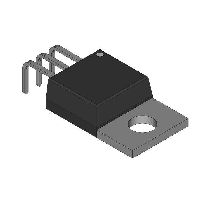
PG-TO-252-3
The IFX7805 is not qualified and manufactured according to the
requirements of Infineon Technologies with regards to automotive and/or
transportation applications. For automotive applications please refer to
the Infineon TLx (TLE, TLS, TLF....) voltage regulator products.
Description
The IFX7805 monolithic 3-terminal positive voltage regulator employs
internal current-limiting, thermal shutdown and safe-area compensation,
making it extremely robust. The IFX7805 is available in a fixed 5V version
and is capable of delivering an output current of 1A. These regulators can
provide local on-card regulation, eliminating the distribution problems
associated with single point regulation. This linear voltage regulator is
designed for a wide variety of applications and suitable for use in harsh
environments. The short-circuit current limit, limits the output current of
the device. The safe-area protection feature limits the internal power
dissipation, in case the internal power dissipation becomes too high, the
thermal shutdown implemented prevents the device from overheating.
PG-TO-220-3
The 5V voltage regulator is available in the TO-252, TO-220 and TO-263
packages.
PG-TO-263-3
Datasheet
2
Rev. 1.0, 2013-07-15
�IFX7805
1.1
Ordering Information
Type
Package
Marking
IFX7805ABTF
PG-TO-252-3
I7805B
IFX7805ABTS
PG-TO-220-3
I7805BTS
IFX7805ABTC
PG-TO-263-3
I7805BTC
Datasheet
3
Rev. 1.0, 2013-07-15
�IFX7805
Block Diagram
2
Block Diagram
IFX7805
IN 1
3
OUT
SOA
Protection
Bias
Thermal
Protection
Startup
Error
Amplifier
Voltage
Reference
2
GND
Figure 1
Datasheet
Block Diagram
4
Rev. 1.0, 2013-07-15
�IFX7805
Pin Configuration
3
Pin Configuration
3.1
Pin Assignment
2
1
1 2
3
3
PG-TO-263-3
PG-TO-252-3
1
2
3
PG-TO-220-3
Figure 2
Pin Configuration
3.2
Pin Definitions and Functions
3
Pin
Symbol
Function
1
IN
Input
The input pin is where the input power is supplied to the device. A capacitor is
required from input to ground. Please refer to the application information section for
more details.“Application Information” on Page 13
2
GND
Ground, Internally connected to thermal tab
3
OUT
Output
The output voltage supplies power to the load. For stability a minimum output
capacitor of 100nF is required from output to ground. Please refer to the application
information section for more details. “Application Information” on Page 13
Datasheet
5
Rev. 1.0, 2013-07-15
�IFX7805
General Product Characteristics
4
General Product Characteristics
4.1
Absolute Maximum Ratings
Table 1
Absolute Maximum Ratings 1)
Tj = -40 °C to +125 °C; all voltages with respect to ground, positive current flowing into pin (unless otherwise
specified)
Pos.
Parameter
Symbol
Limit Values
Unit
Conditions
V
–
Min.
Max.
VIN
-0.3
35
IOUT
Internally Limited
A
–
Tj
Tstg
-40
150
°C
–
-50
150
°C
–
VESD
VESD
-2
2
kV
HBM2)
-1
1
kV
CDM3)
Voltage Input
4.1.1
Voltage
Output Current
4.1.2
Current
Temperatures
4.1.3
Junction Temperature
4.1.4
Storage Temperature
ESD Susceptibility
4.1.5
All Pins
4.1.6
All Pins
1) Not subject to production test, specified by design
2) ESD susceptibility, HBM according to ANSI/ESDA/JEDEC JS-001(1.5 kΩ, 100 pF)
3) ESD susceptibility, Charged Device Model “CDM” according to JEDEC JESD22-C101
Note: Stresses above the ones listed here may cause permanent damage to the device. Exposure to absolute
maximum rating conditions for extended periods may affect device reliability.
Note: Integrated protection functions are designed to prevent IC destruction under fault conditions described in the
data sheet. Fault conditions are considered as “outside” normal operating range. Protection functions are
not designed for continuous repetitive operation.
4.2
Functional Range
Table 2
Functional Range
Pos.
Parameter
Symbol
Limit Values
Unit
Conditions
VOUT + Vdr 35
V
1)
-40
°C
–
Min.
4.2.1
Input Voltage Range
4.2.2
Junction temperature
VIN
Tj
Max.
125
1) Output current is limited internally and depends on the maximum voltage, see Electrical Characteristics for more details.
Note: Within the functional or operating range, the IC operates as described in the circuit description. The electrical
characteristics are specified within the conditions given in the Electrical Characteristics table.
Datasheet
6
Rev. 1.0, 2013-07-15
�IFX7805
General Product Characteristics
4.3
Thermal Resistance
Note: This thermal data was generated in accordance with JEDEC JESD51 standards. For more information, go
to www.jedec.org.
Pos.
Parameter
Symbol
Limit Values
Unit
Conditions
Min.
Typ.
Max.
–
4
–
K/W
–
–
27
–
K/W
–2)
4.3.3
–
113
–
K/W
Footprint Only
4.3.4
–
52
–
K/W
300mm2 heatsink
area on PCB3)
4.3.5
–
42
–
K/W
600mm2 heatsink
area on PCB
–
4
–
K/W
–
–
23
–
K/W
–
4.3.8
–
76
–
K/W
Footprint Only
4.3.9
–
44
–
K/W
300mm2 heatsink
area on PCB
4.3.10
–
35
–
K/W
600mm2 heatsink
area on PCB
–
4
–
K/W
–
–
41
–
K/W
–
4.3.13
–
91
–
K/W
Footprint Only
4.3.14
–
63
–
K/W
300mm2 heatsink
area on PCB
4.3.15
–
58
–
K/W
600mm2 heatsink
area on PCB
PG-TO-252-3
4.3.1
Junction to Case1)
4.3.2
Junction to Ambient
RthJC
RthJA
PG-TO-263-3
4.3.6
Junction to Case
4.3.7
Junction to Ambient
RthJC
RthJA
PG-TO-220-3
4.3.11
Junction to Case
4.3.12
Junction to Ambient
RthJC
RthJA
1) Not subject to production test, specified by design.
2) Specified RthJA value is according to JEDEC JESD51-5,-7 at natural convection on FR4 2s2p board. The product (chip and
package) was simulated on a 76.2 x 114.3 x 1.5 mm3 board with 2 inner copper layers (2 x 70µm Cu, 2 x 35 µm Cu).
3) Specified RthJA value is according to JEDEC JESD51-3 at natural convection on FR4 1s0p board. The product (chip and
package) was simulated on a 76.2 x 114.3 x 1.5 mm3 board with 1 copper layer (1 x 70µm Cu)
Datasheet
7
Rev. 1.0, 2013-07-15
�IFX7805
Electrical Characteristics
5
Electrical Characteristics
5.1
IFX7805
Table 3
Electrical Characteristics
-40 °C < Tj < 125 °C; VIN = 10V, CIN = 0.33µF, COUT = 100nF; unless otherwise specified.
Pos.
5.1.1
Parameter
Output Voltage
Symbol
VOUT
5.1.2
5.1.3
Line Regulation
Limit Values
Unit
Test Condition
Min.
Typ.
Max.
4.81
5.00
5.19
V
IOUT = 1 A, Tj = 25 °C
4.80
5.00
5.20
V
5 mA ≤ IOUT ≤ 1 A,
7.5 V ≤ VIN ≤ 20 V
PD ≤ 15 W
4
mV
IOUT = 1 A
8 V ≤ VIN ≤ 12 V,
Tj = 25 °C
∆VOUT,LINE
5.1.4
1
10
mV
IOUT = 1A,
7.5 V ≤ VIN ≤ 20 V
Tj = 25 °C
5.1.5
3
10
mV
IOUT = 1 A
7.5 V ≤ VIN≤ 20 V
10
15
mV
5.0 mA ≤ IOUT ≤ 1 A,
Tj= 25 °C
15
mV
5.0 mA ≤ IOUT ≤ 1 A
V
IOUT = 1 A, Tj = 25 °C
5.1.6
Load Regulation
∆VOUT,LOAD
5.1.7
5.1.8
Dropout Voltage
Vdr
2
5.1.9
Quiescent Current
Iq
3.5
5.0
mA
IOUT = 1 A Tj = 25 °C
3.5
6.0
mA
IOUT = 1 A
mA
5.0 mA ≤ IOUT ≤ 1 A
5.1.10
5.1.11
Quiescent Current Change
∆ Iq
1.0
5.1.12
0.5
0.8
mA
IOUT = 1 A
7.5 V ≤VIN ≤ 20 V
Tj = 25 °C
5.1.13
0.5
1.0
mA
IOUT = 0.5 A
8 V ≤ VIN ≤ 25 V
40
µV
10 Hz ≤ f ≤ 100 kHz,
Tj = 25 °C1)
dB
f = 120 Hz, IOUT = 10 mA
Tj = 25 °C2)
5.1.14
Output Noise Voltage
VNoise
5.1.15
Ripple Rejection
PSRR
68
75
5.1.16
Short Circuit Current
0.5
0.8
1.2
A
VIN = 35 V, Tj = 25 °C
5.1.17
Peak Output Current
2.0
2.4
2.9
A
Tj = 25 °C
5.1.18
Input Voltage Required to
Maintain Line Regulation
ISC
IPK
VIN,MIN
V
Tj = 25 °C
7.5
1) Not subject to production test
2) Not subject to production test
Note: The listed characteristics are ensured over the operating range of the integrated circuit. Typical
characteristics specified mean values expected over the production spread. If not otherwise specified,
typical characteristics apply at TA = 25 °C and the given supply voltage.
Datasheet
8
Rev. 1.0, 2013-07-15
�IFX7805
Electrical Characteristics
5.1.1
Typical Performance Graphs
Typical Performance Characteristics
Output Voltage VOUT Vs
Junction Temperature Tj (VIN = 12V)
5
5
4.98
4.98
4.96
4.96
4.94
4.94
4.92
4.92
VOUT [V]
VOUT [V]
Output Voltage VOUT Vs
Junction Temperature Tj (VIN = 7.5V)
4.9
4.9
4.88
4.88
4.86
4.86
4.84
4.84
IOUT = 5 mA
4.82
IOUT = 5 mA
IOUT = 100 mA
4.82
IOUT = 1 A
4.8
0
IOUT = 100 mA
IOUT = 1 A
50
Tj [°C]
4.8
100
Output Voltage VOUT Vs
Junction Temperature Tj (VIN = 20V)
0
50
Tj [°C]
100
Drop Voltage VDR Vs
Junction Temperature Tj
5
3
4.98
2.8
4.96
2.6
4.94
2.4
4.92
2.2
VDR [V]
VOUT [V]
IOUT = 100 mA
4.9
IOUT = 1 A
2
4.88
1.8
4.86
1.6
4.84
IOUT = 500 mA
1.4
IOUT = 5 mA
4.82
IOUT = 100 mA
1.2
IOUT = 1 A
4.8
Datasheet
0
50
Tj [°C]
1
100
9
0
50
Tj [°C]
100
Rev. 1.0, 2013-07-15
�IFX7805
Electrical Characteristics
Drop Voltage VDR Vs
Output Current IOUT
Current Limit
Output Current IOUT Vs Input Voltage VIN
3
4
Tj = −40°C
2.8
Tj = −40°C
Tj = 25°C
Tj = 25°C
3.5
Tj = 125°C
2.6
Tj = 125°C
3
2.4
2.5
IOUT [A]
VDR [V]
2.2
2
1.8
2
1.5
1.6
1
1.4
0.5
1.2
1
0
0.2
0.4
0.6
IOUT [A]
0.8
0
1
Line Regulation
Output Current IOUT = 5mA
0
5
10
15
20
VIN [V]
25
30
35
Line Regulation
Output Current IOUT = 1A
15
15
Tj = −40°C
Tj = −40°C
Tj = 25°C
Tj = 25°C
Tj = 125°C
Tj = 125°C
ΔVOUT,Line [mV]
10
ΔVOUT,Line [mV]
10
5
0
5
8
Datasheet
10
12
14
VIN [V]
16
18
0
20
10
8
10
12
14
VIN [V]
16
18
20
Rev. 1.0, 2013-07-15
�IFX7805
Electrical Characteristics
Load Regulation
Input Voltage VIN = 7.5V
Load Regulation
Input Voltage VIN = 20V
15
15
Tj = −40°C
Tj = −40°C
Tj = 25°C
Tj = 25°C
Tj = 125°C
Tj = 125°C
ΔVOUT,Load [mV]
10
ΔVOUT,Load [mV]
10
5
0
5
0
200
400
600
IOUT [mA]
800
0
1000
Current Consumption Iq Vs
Output Current IOUT
0
200
800
1000
Current Consumption Iq Vs
Input Voltage VIN
7
7
Tj = −40°C
6.5
Tj = −40°C
Tj = 25°C
Tj = 25°C
6
Tj = 125°C
6
Tj = 125°C
5
5.5
5
4
Iq [mA]
Iq [mA]
400
600
IOUT [mA]
4.5
3
4
3.5
2
3
1
2.5
2
0
Datasheet
0.2
0.4
0.6
IOUT [A]
0.8
0
1
11
8
10
12
14
VIN [V]
16
18
20
Rev. 1.0, 2013-07-15
�IFX7805
Electrical Characteristics
Power Supply Rejection Ratio
Output Current IOUT = 10 mA
ESR Tunnel
ESR(COUT) Vs Output Current IOUT
90
12
Max ESR
80
10
70
8
ESR(COUT) [Ω]
PSRR [dB]
60
50
40
6
30
4
20
Tj = −40°C
10
2
Tj = 25°C
COUT = 100 nF .
Tj = 125°C
0
1
10
2
10
3
4
10
10
Frequency [Hz]
5
0
1m
6
10
10
10m
100m
1
IOUT [A]
Line Transient Response
Load Transient Response
18
1
IOUT [A]
VIN [V]
16
14
12
0.5
10
8
4
6
8
10
12
t [us]
14
16
18
0
20
VOUT [V]
VOUT [V]
10
20
30
40
t [us]
50
60
70
80
0
10
20
30
40
t [us]
50
60
70
80
5.2
4.95
4.9
4.85
4.8
4.75
0
4
6
Datasheet
8
10
12
t [us]
14
16
18
5
4.8
4.6
20
12
Rev. 1.0, 2013-07-15
�IFX7805
Application Information
6
Application Information
Note: The following information is given as a hint for the implementation of the device only and shall not be
regarded as a description or warranty of a certain functionality, condition or quality of the device.
6.1
Design Considerations
The IFX7805 linear voltage regulator has an in built thermal overload protection circuitry that shuts down the circuit
when subjected to an excessive power overload condition. Thermal shutdown protects the regulator from
immediate destruction due to high temperature conditions by turning it off. The thermal shutdown is set to a typical
value of 175°C. Operating a linear regulator over the maximum junction temperature significantly reduces the life
time of the device and pushes the operating variables outside their specified limits. The device also has an unbolt
short circuit protection feature that keeps the output current within the specified bounds to protect both the
regulator and the load. The safe-area compensation reduces the output short-circuit current as the voltage across
the power stage is increased.
It is recommended that the regulator input is bypassed with a capacitor if the regulator is connected to the power
supply filter with long lengths, or if the load capacitance at the output is large. A 0.33µF or larger tantalum or other
capacitor, with a low internal impedance at high frequencies, should be chosen. The bypass capacitor should be
mounted with the shortest possible leads directly across the input terminals of the regulator.
Fixed Output Regulator
VOUT
VIN
IFX7805
CIN = 0.33 µF
COUT = 0.1 µF
1) A capacitor at the output is recommended for improved transient response
.
2) An output capacitor is required if the regulator is located at an appreciable distance from the supply filter
Figure 3
Datasheet
Typical Application Diagram
13
Rev. 1.0, 2013-07-15
�IFX7805
Package Outlines
7
Package Outlines
6.5 +0.15
-0.10
2.3 +0.05
-0.10
4.57
0.9 +0.08
-0.04
B
0.51 MIN.
0.15 MAX.
per side
5.4
0.8 ±0.15
9.9 ±0.5
6.22 -0.2
1 ±0.1
A
±0.1
3x
0.75 ±0.1
0...0.15
0.5 +0.08
-0.04
2.28
1 ±0.1
0.25
M
A B
0.1
All metal surfaces tin plated, except area of cut.
Figure 4
Datasheet
PG-TO-252-3 (Plastic Small Outline Transistor)
14
Rev. 1.0, 2013-07-15
�IFX7805
Package Outlines
10 ±0.2
A
9.9 ±0.2
B
2.8 ±0.2
4.4
1.27±0.1
0.05
C
0...0.15
13.5 ±0.5
4.55 ±0.2
2.4
9.25 ±0.2
1)
0...0.3
12.95
15.65 ±0.3
17±0.3
8.5 1)
3.7 -0.15
0.5 ±0.1
3x
0.75 ±0.1
2.4
1.05
2x 2.54
1)
Figure 5
Datasheet
0.25
M
A B C
Typical
All metal surfaces tin plated, except area of cut.
Metal surface min. x=7.25, y=12.3
PG-TO-220-3 (Plastic Small Outline Transistor)
15
Rev. 1.0, 2013-07-15
�IFX7805
Package Outlines
4.4
10 ±0.2
1.27 ±0.1
B
0.1
A
8.5 1)
0.05
2.4
2.7 ±0.3
4.7 ±0.5
7.55 1)
9.25 ±0.2
(15)
1 ±0.3
0...0.3
0...0.15
0.75 ±0.1
0.5 ±0.1
1.05
8˚ MAX.
2.54
5.08
0.25
M
A B
1) Typical
All metal surfaces: tin plated, except area of cut.
Metal surface min. x=7.25, y=6.9
Figure 6
0.1 B
GPT09362
PG-TO-263-3 (Plastic Small Outline Transistor)
Green Product (RoHS compliant)
To meet the world-wide customer requirements for environmentally friendly products and to be compliant with
government regulations the device is available as a green product. Green products are RoHS-Compliant (i.e
Pb-free finish on leads and suitable for Pb-free soldering according to IPC/JEDEC J-STD-020).
For further information on alternative packages, please visit our website:
http://www.infineon.com/packages.
Datasheet
16
Dimensions in mm
Rev. 1.0, 2013-07-15
�IFX7805
Revision History
8
Revision History
Revision
Date
Changes
1.0
2013-07-15
Datasheet - Initial Release
Datasheet
17
Rev. 1.0, 2013-07-15
�Edition 2013-07-15
Published by
Infineon Technologies AG
81726 Munich, Germany
© 2011 Infineon Technologies AG
All Rights Reserved.
Legal Disclaimer
The information given in this document shall in no event be regarded as a guarantee of conditions or
characteristics. With respect to any examples or hints given herein, any typical values stated herein and/or any
information regarding the application of the device, Infineon Technologies hereby disclaims any and all warranties
and liabilities of any kind, including without limitation, warranties of non-infringement of intellectual property rights
of any third party.
Information
For further information on technology, delivery terms and conditions and prices, please contact the nearest
Infineon Technologies Office (www.infineon.com).
Warnings
Due to technical requirements, components may contain dangerous substances. For information on the types in
question, please contact the nearest Infineon Technologies Office.
The Infineon Technologies component described in this Data Sheet may be used in life-support devices or systems
and/or automotive, aviation and aerospace applications or systems only with the express written approval of
Infineon Technologies, if a failure of such components can reasonably be expected to cause the failure of that lifesupport automotive, aviation and aerospace device or system or to affect the safety or effectiveness of that device
or system. Life support devices or systems are intended to be implanted in the human body or to support and/or
maintain and sustain and/or protect human life. If they fail, it is reasonable to assume that the health of the user
or other persons may be endangered.
�