IKP20N60T, IKB20N60T
TrenchStop Series
IKW20N60T
Low Loss DuoPack : IGBT in Trench and Fieldstop technology
with soft, fast recovery anti-parallel EmCon HE diode
•
•
•
•
•
•
•
•
•
•
C
Very low VCE(sat) 1.5 V (typ.)
Maximum Junction Temperature 175 °C
Short circuit withstand time – 5µs
Designed for :
- Frequency Converters
- Uninterrupted Power Supply
Trench and Fieldstop technology for 600 V applications offers :
- very tight parameter distribution
- high ruggedness, temperature stable behavior
- very high switching speed
- low VCE(sat)
Positive temperature coefficient in VCE(sat)
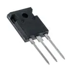
P-TO-220-3-1
Low EMI
(TO-220AB)
Low Gate Charge
Very soft, fast recovery anti-parallel EmCon HE diode
Complete product spectrum and PSpice Models : http://www.infineon.com/igbt/
Type
G
E
P-TO-247-3-1
(TO-220AC)
P-TO-263-3-2 (D²-PAK)
(TO-263AB)
VCE
IC
VCE(sat),Tj=25°C
Tj,max
Marking Code
Package
Ordering Code
IKP20N60T
600V
20A
1.5V
175°C
K20T60
TO-220
Q67040S4715
IKB20N60T
600V
20A
1.5V
175°C
K20T60
TO-263
Q67040S4713
IKW20N60T
600V
20A
1.5V
175°C
K20T60
TO-247
Q67040S4716
Maximum Ratings
Parameter
Symbol
Collector-emitter voltage
VCE
DC collector current, limited by Tjmax
IC
Value
Unit
600
V
A
TC = 25°C
40
TC = 100°C
20
Pulsed collector current, tp limited by Tjmax
ICpuls
60
Turn off safe operating area (VCE ≤ 600V, Tj ≤ 175°C)
-
60
Diode forward current, limited by Tjmax
IF
TC = 25°C
40
TC = 100°C
20
Diode pulsed current, tp limited by Tjmax
IFpuls
60
Gate-emitter voltage
VGE
±20
V
tSC
5
µs
Power dissipation TC = 25°C
Ptot
166
W
Operating junction temperature
Tj
-40...+175
°C
Storage temperature
Tstg
-55...+175
Soldering temperature, 1.6mm (0.063 in.) from case for 10s
-
Short circuit withstand time
1)
VGE = 15V, VCC ≤ 400V, Tj ≤ 150°C
1)
260
Allowed number of short circuits: 1s.
Power Semiconductors
1
Rev. 2.2 Dec-04
�IKP20N60T, IKB20N60T
TrenchStop Series
IKW20N60T
Thermal Resistance
Parameter
Symbol
Conditions
Max. Value
Unit
RthJC
TO-220-3-1
0.9
K/W
Characteristic
IGBT thermal resistance,
junction – case
TO-247-3-1
TO-263-3-2
Diode thermal resistance,
RthJCD
TO-220-3-1
junction – case
1.5
TO-247-3-1
TO-263-3-2
Thermal resistance,
RthJA
TO-220-3-1
62
TO-247-3-1
40
TO-263-3-2 (6cm² Cu)
40
junction – ambient
Electrical Characteristic, at Tj = 25 °C, unless otherwise specified
Parameter
Symbol
Conditions
Value
min.
Typ.
max.
600
-
-
T j = 25° C
-
1.5
2.05
T j = 17 5° C
-
1.9
-
T j = 25° C
-
1.65
2.05
T j = 17 5° C
-
1.6
-
4.1
4.9
5.7
Unit
Static Characteristic
Collector-emitter breakdown voltage
V ( B R ) C E S V G E = 0V, I C = 0. 2mA
Collector-emitter saturation voltage
VCE(sat)
Diode forward voltage
VF
V
V G E = 15V, I C = 20A
V G E = 0V, I F = 2 0 A
Gate-emitter threshold voltage
VGE(th)
I C = 29 0µ A, V C E =V G E
Zero gate voltage collector current
ICES
V C E = 600V ,
V G E = 0V
µA
T j = 25° C
-
-
40
T j = 17 5° C
-
-
1000
Gate-emitter leakage current
IGES
V C E = 0V ,V G E = 2 0V
-
-
100
nA
Transconductance
gfs
V C E = 20V, I C = 20A
-
11
-
S
Integrated gate resistor
RGint
Power Semiconductors
-
2
Ω
Rev. 2.2 Dec-04
�IKP20N60T, IKB20N60T
TrenchStop Series
IKW20N60T
Dynamic Characteristic
Input capacitance
Ciss
V C E = 25V,
-
1100
-
Output capacitance
Coss
V G E = 0V,
-
71
-
Reverse transfer capacitance
Crss
f= 1 M Hz
-
-
Gate charge
QGate
V C C = 4 80V, I C = 20A
-
32
120
-
nC
-
7
-
nH
-
183.3
-
A
pF
V G E = 1 5V
Internal emitter inductance
LE
measured 5mm (0.197 in.) from case
T O - 2 20-3- 1
T O - 2 47-3- 1
T O - 2 63-3- 2
Short circuit collector current
1)
IC(SC)
V G E = 1 5V,t S C ≤5µs
V C C = 400V,
T j ≤ 150° C
Switching Characteristic, Inductive Load, at Tj=25 °C
Parameter
Symbol
Conditions
Value
min.
Typ.
max.
Unit
IGBT Characteristic
Turn-on delay time
td(on)
Rise time
tr
Turn-off delay time
td(off)
Fall time
tf
Turn-on energy
Eon
Turn-off energy
Eoff
Total switching energy
Ets
-
18
-
-
14
-
-
199
-
-
42
-
T j = 25° C,
V C C = 4 00V, I C = 20A,
V G E = 0/ 1 5V ,
RG=12 Ω,
L σ 2 ) = 131nH,
C σ 2 ) =31pF
Energy losses include
“tail” and diode
reverse recovery.
-
0.31
-
-
0.46
-
-
0.77
-
ns
mJ
Anti-Parallel Diode Characteristic
Diode reverse recovery time
trr
T j = 25° C,
-
41
-
ns
Diode reverse recovery charge
Qrr
V R = 4 00V, I F = 2 0A ,
-
0.31
-
µC
Diode peak reverse recovery current
Irrm
di F / dt = 88 0A / µs
-
13.3
-
A
Diode peak rate of fall of reverse
recovery current during t b
di r r / d t
-
711
-
A/µs
1)
2)
Allowed number of short circuits: 1s.
Leakage inductance L σ and Stray capacity C σ due to dynamic test circuit in Figure E.
Power Semiconductors
3
Rev. 2.2 Dec-04
�IKP20N60T, IKB20N60T
TrenchStop Series
IKW20N60T
Switching Characteristic, Inductive Load, at Tj=175 °C
Parameter
Symbol
Conditions
Value
min.
Typ.
max.
-
18
-
-
18
-
-
223
-
Unit
IGBT Characteristic
Turn-on delay time
td(on)
Rise time
tr
Turn-off delay time
td(off)
Fall time
tf
Turn-on energy
Eon
Turn-off energy
Eoff
Total switching energy
Ets
T j = 17 5° C,
V C C = 4 00V, I C = 20A,
V G E = 0/ 1 5V ,
R G = 12 Ω
L σ 1 ) = 131nH,
C σ 1 ) =31pF
Energy losses include
“tail” and diode
reverse recovery.
Diode reverse recovery time
trr
Diode reverse recovery charge
ns
-
76
-
-
0.51
-
-
0.64
-
-
1.15
-
T j = 17 5° C
-
176
-
ns
Qrr
V R = 4 00V, I F = 2 0A ,
-
1.46
-
µC
Diode peak reverse recovery current
Irrm
di F / dt = 88 0A / µs
-
18.9
-
A
Diode peak rate of fall of reverse
recovery current during t b
di r r / d t
-
467
-
A/µs
mJ
Anti-Parallel Diode Characteristic
1)
Leakage inductance L σ and Stray capacity C σ due to dynamic test circuit in Figure E.
Power Semiconductors
4
Rev. 2.2 Dec-04
�IKP20N60T, IKB20N60T
TrenchStop Series
IKW20N60T
t p=2µs
10µs
50A
T C =80°C
40A
T C =110°C
30A
20A
Ic
10A
0A
10H z
IC, COLLECTOR CURRENT
IC, COLLECTOR CURRENT
60A
10A
50µs
1A
1ms
10ms
DC
Ic
100H z
1kH z
10kH z
0.1A
1V
100kH z
f, SWITCHING FREQUENCY
Figure 1. Collector current as a function of
switching frequency
(Tj ≤ 175°C, D = 0.5, VCE = 400V,
VGE = 0/+15V, RG = 12Ω)
10V
100V
1000V
VCE, COLLECTOR-EMITTER VOLTAGE
Figure 2. Safe operating area
(D = 0, TC = 25°C, Tj ≤175°C;
VGE=15V)
160W
30A
IC, COLLECTOR CURRENT
Ptot,
POWER DISSIPATION
140W
120W
100W
80W
60W
40W
20A
15A
10A
5A
20W
0W
25°C
25A
50°C
75°C
0A
25°C
100°C 125°C 150°C
TC, CASE TEMPERATURE
Figure 3. Power dissipation as a function of
case temperature
(Tj ≤ 175°C)
Power Semiconductors
5
75°C
125°C
TC, CASE TEMPERATURE
Figure 4. Collector current as a function of
case temperature
(VGE ≥ 15V, Tj ≤ 175°C)
Rev. 2.2 Dec-04
�IKP20N60T, IKB20N60T
TrenchStop Series
IKW20N60T
50A
V GE =20V
V GE =20V
40A
IC, COLLECTOR CURRENT
IC, COLLECTOR CURRENT
50A
15V
13V
30A
11V
9V
20A
7V
10A
30A
11V
20A
7V
9V
0A
0V
1V
2V
3V
0V
35A
30A
25A
20A
15A
10A
T J = 1 7 5 °C
5A
2 5 °C
0V
2V
4V
6V
8V
VGE, GATE-EMITTER VOLTAGE
Figure 7. Typical transfer characteristic
(VCE=10V)
Power Semiconductors
1V
2V
3V
4V
VCE, COLLECTOR-EMITTER VOLTAGE
Figure 6. Typical output characteristic
(Tj = 175°C)
VCE(sat), COLLECTOR-EMITT SATURATION VOLTAGE
VCE, COLLECTOR-EMITTER VOLTAGE
Figure 5. Typical output characteristic
(Tj = 25°C)
IC, COLLECTOR CURRENT
15V
13V
10A
0A
0A
40A
2.5V
IC =40A
2.0V
1.5V
IC =20A
1.0V
IC =10A
0.5V
0.0V
0°C
50°C
100°C
150°C
TJ, JUNCTION TEMPERATURE
Figure 8. Typical collector-emitter
saturation voltage as a function of
junction temperature
(VGE = 15V)
6
Rev. 2.2 Dec-04
�IKP20N60T, IKB20N60T
TrenchStop Series
IKW20N60T
t d(off)
100ns
t, SWITCHING TIMES
t, SWITCHING TIMES
t d(off)
tf
t d(on)
10ns
tf
100ns
t d(on)
tr
tr
1ns
0A
5A
10A
15A
20A
25A
30A
10ns
35A
IC, COLLECTOR CURRENT
Figure 9. Typical switching times as a
function of collector current
(inductive load, TJ=175°C,
VCE = 400V, VGE = 0/15V, RG = 12Ω,
Dynamic test circuit in Figure E)
10Ω
20Ω
30Ω
40Ω
50Ω
60Ω
70Ω
RG, GATE RESISTOR
Figure 10. Typical switching times as a
function of gate resistor
(inductive load, TJ = 175°C,
VCE= 400V, VGE = 0/15V, IC = 20A,
Dynamic test circuit in Figure E)
t, SWITCHING TIMES
t d(off)
100ns
tf
t d(on)
tr
10ns
25°C
50°C
75°C
6V
m ax.
typ.
5V
4V
m in.
3V
2V
1V
0V
-50°C
100°C 125°C 150°C
TJ, JUNCTION TEMPERATURE
Figure 11. Typical switching times as a
function of junction temperature
(inductive load, VCE = 400V,
VGE = 0/15V, IC = 20A, RG=12Ω,
Dynamic test circuit in Figure E)
Power Semiconductors
VGE(th), GATE-EMITT TRSHOLD VOLTAGE
7V
0°C
50°C
100°C
150°C
TJ, JUNCTION TEMPERATURE
Figure 12. Gate-emitter threshold voltage as
a function of junction temperature
(IC = 0.29mA)
7
Rev. 2.2 Dec-04
�IKP20N60T, IKB20N60T
TrenchStop Series
IKW20N60T
*) Eon and Ets include losses
due to diode recovery
2.4m J
Ets*
2.0mJ
1.6mJ
1.2mJ
Eoff
0.8mJ
0.4mJ
Eon*
0.0mJ
0A
5A
10A
15A
25A
30A
35A
*) Eon and Ets include losses
due to diode recovery
1.6m J
E off
1.2m J
0.8m J
0.4m J
E on *
0Ω
15Ω
30Ω
45Ω
60Ω
RG, GATE RESISTOR
Figure 14. Typical switching energy losses
as a function of gate resistor
(inductive load, TJ = 175°C,
VCE = 400V, VGE = 0/15V, IC = 20A,
Dynamic test circuit in Figure E)
2.0m J
1.8m J
Ets*
E, SWITCHING ENERGY LOSSES
E, SWITCHING ENERGY LOSSES
1.0mJ
0.8mJ
Eoff
0.4mJ
0.2mJ
E ts *
2.0m J
0.0m J
20A
IC, COLLECTOR CURRENT
Figure 13. Typical switching energy losses
as a function of collector current
(inductive load, TJ = 175°C,
VCE = 400V, VGE = 0/15V, RG = 12Ω,
Dynamic test circuit in Figure E)
0.6mJ
*) E on a nd E ts include losses
d ue to diode re co ve ry
E, SWITCHING ENERGY LOSSES
E, SWITCHING ENERGY LOSSES
2.4mJ
Eon*
*) E on and E ts include losses
due to diode recovery
1.6m J
1.4m J
1.2m J
1.0m J E ts *
E off
0.8m J
0.6m J
0.4m J
E on *
0.2m J
0.0mJ
25°C
50°C
75°C
0.0m J
300V
100°C 125°C 150°C
TJ, JUNCTION TEMPERATURE
Figure 15. Typical switching energy losses
as a function of junction
temperature
(inductive load, VCE = 400V,
VGE = 0/15V, IC = 20A, RG = 12Ω,
Dynamic test circuit in Figure E)
Power Semiconductors
350V
400V
450V
500V
550V
VCE, COLLECTOR-EMITTER VOLTAGE
Figure 16. Typical switching energy losses
as a function of collector emitter
voltage
(inductive load, TJ = 175°C,
VGE = 0/15V, IC = 20A, RG = 12Ω,
Dynamic test circuit in Figure E)
8
Rev. 2.2 Dec-04
�IKP20N60T, IKB20N60T
TrenchStop Series
IKW20N60T
1nF
VGE, GATE-EMITTER VOLTAGE
C iss
c, CAPACITANCE
1 5V
1 20V
4 80V
1 0V
100pF
C oss
C rss
5V
0V
0nC
30n C
6 0nC
9 0nC
10pF
120 nC
QGE, GATE CHARGE
Figure 17. Typical gate charge
(IC=20 A)
0V
10V
20V
30V
40V
VCE, COLLECTOR-EMITTER VOLTAGE
Figure 18. Typical capacitance as a function
of collector-emitter voltage
(VGE=0V, f = 1 MHz)
SHORT CIRCUIT WITHSTAND TIME
300A
250A
200A
150A
100A
tSC,
IC(sc), short circuit COLLECTOR CURRENT
12µs
50A
0A
12V
14V
16V
8µs
6µs
4µs
2µs
0µs
10V
18V
VGE, GATE-EMITTETR VOLTAGE
Figure 19. Typical short circuit collector
current as a function of gateemitter voltage
(VCE ≤ 400V, Tj ≤ 150°C)
Power Semiconductors
10µs
11V
12V
13V
14V
VGE, GATE-EMITETR VOLTAGE
Figure 20. Short circuit withstand time as a
function of gate-emitter voltage
(VCE=600V, start at TJ=25°C,
TJmax