IKW50N65ET7
Low Loss Duopack: IGBT 7
Low Loss Duopack: IGBT 7 with Trench and Fieldstop technology
Features
•
•
•
•
•
•
•
•
•
•
•
•
VCE = 650 V
IC = 50 A
Very Low VCEsat
Low turn-off losses
Short tail current
Reduced EMI
Humidity robust design
Very soft, fast recovery antiparallel diode
Maximum junction temperature Tvjmax = 175°C
Qualified according to JEDEC for target applications
Pb-free lead plating; RoHS compliant
Complete product spectrum and PSpice Models: http://www.infineon.com/igbt7/
G
C
E
Potential applications
•
•
•
•
•
•
Servo Drives
General Purpose Drives (GPD)
Industrial UPS
Industrial SMPS
Solar Optimizer
Solar String Inverter
Product validation
• Product Validation: Qualified for industrial applications according to the relevant tests of
JEDEC47/20/22
Description
Package pin definition:
• Pin C & backside - Collector
• Pin E - Emitter
• Pin G - Gate
C
G
E
Type
Package
Marking
IKW50N65ET7
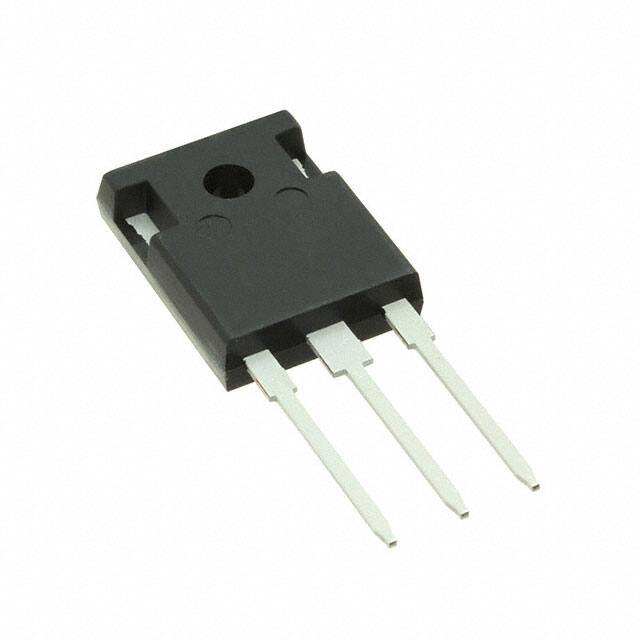
PG-TO247-3
K50EET7
Datasheet
www.infineon.com
Please read the Important Notice and Warnings at the end of this document
1.00
2021-06-29
�IKW50N65ET7
Low Loss Duopack: IGBT 7
Table of contents
Table of contents
Description . . . . . . . . . . . . . . . . . . . . . . . . . . . . . . . . . . . . . . . . . . . . . . . . . . . . . . . . . . . . . . . . . . . . . . . . . . . . . . . . . . 1
Features . . . . . . . . . . . . . . . . . . . . . . . . . . . . . . . . . . . . . . . . . . . . . . . . . . . . . . . . . . . . . . . . . . . . . . . . . . . . . . . . . . . . .1
Potential applications . . . . . . . . . . . . . . . . . . . . . . . . . . . . . . . . . . . . . . . . . . . . . . . . . . . . . . . . . . . . . . . . . . . . . . . 1
Product validation . . . . . . . . . . . . . . . . . . . . . . . . . . . . . . . . . . . . . . . . . . . . . . . . . . . . . . . . . . . . . . . . . . . . . . . . . . . 1
Table of contents . . . . . . . . . . . . . . . . . . . . . . . . . . . . . . . . . . . . . . . . . . . . . . . . . . . . . . . . . . . . . . . . . . . . . . . . . . . . 2
1
Package . . . . . . . . . . . . . . . . . . . . . . . . . . . . . . . . . . . . . . . . . . . . . . . . . . . . . . . . . . . . . . . . . . . . . . . . . . . . . . . . . . . . . 3
2
IGBT . . . . . . . . . . . . . . . . . . . . . . . . . . . . . . . . . . . . . . . . . . . . . . . . . . . . . . . . . . . . . . . . . . . . . . . . . . . . . . . . . . . . . . . . .3
3
Diode . . . . . . . . . . . . . . . . . . . . . . . . . . . . . . . . . . . . . . . . . . . . . . . . . . . . . . . . . . . . . . . . . . . . . . . . . . . . . . . . . . . . . . . .6
4
Characteristics diagrams . . . . . . . . . . . . . . . . . . . . . . . . . . . . . . . . . . . . . . . . . . . . . . . . . . . . . . . . . . . . . . . . . . . . . 9
5
Package outlines . . . . . . . . . . . . . . . . . . . . . . . . . . . . . . . . . . . . . . . . . . . . . . . . . . . . . . . . . . . . . . . . . . . . . . . . . . . .16
6
Testing conditions . . . . . . . . . . . . . . . . . . . . . . . . . . . . . . . . . . . . . . . . . . . . . . . . . . . . . . . . . . . . . . . . . . . . . . . . . . 17
Revision history . . . . . . . . . . . . . . . . . . . . . . . . . . . . . . . . . . . . . . . . . . . . . . . . . . . . . . . . . . . . . . . . . . . . . . . . . . . . 18
Disclaimer . . . . . . . . . . . . . . . . . . . . . . . . . . . . . . . . . . . . . . . . . . . . . . . . . . . . . . . . . . . . . . . . . . . . . . . . . . . . . . . . . . 19
Datasheet
2
1.00
2021-06-29
�IKW50N65ET7
Low Loss Duopack: IGBT 7
1 Package
1
Package
Table 1
Characteristic values
Parameter
Symbol Note or test condition
Values
Min.
Internal emitter inductance
measured 5 mm (0.197 in)
from case
LE
Storage temperature
Tstg
Thermal resistance,
junction-ambient
2
13.0
-55
nH
°C
260
°C
M
0.6
Nm
Rth(j-a)
40
K/W
wave soldering 1.6 mm (0.063 in.) from case
for 10 s
IGBT
Table 2
Maximum rated values
Parameter
Collector-emitter voltage
Symbol Note or test condition
VCE
DC collector current, limited
by Tvjmax
IC
Pulsed collector current, tp
limited by Tvjmax 1)
ICpuls
Turn-off safe operating
area2)
Values
Unit
650
V
TC = 25 °C
80
A
TC = 100 °C
59.7
Tvj ≥ 25 °C
limited by bondwire
VCE ≤ 650 V, tP = 1 µs, Tvj ≤ 175 °C
Gate-emitter voltage
VGE
Transient gate-emitter
voltage
VGE
tp ≤ 10 µs, D < 0.010
Short circuit withstand time
tSC
VGE = 15 V, Allowed
VCC ≤ 330 V,
number of short circuits Tvj = 100 °C
< 1000, Time between
VCC ≤ 400 V,
short circuits ≥ 1.0 s
Tvj = 150 °C
Power dissipation
1)
2)
Max.
150
Soldering temperature
Mounting torque, M3 screw
Maximum of mounting
processes: 3
Typ.
Unit
Ptot
150
A
150
A
±20
V
±30
V
5
µs
3
TC = 25 °C
273
TC = 100 °C
136
W
Defined by design. Not subject to production test.
Clamped inductive load current test for each device, IC=150A, VCC=400V, Tc=25°C, VGE=20V, L=80µH, RG=10Ω
Datasheet
3
1.00
2021-06-29
�IKW50N65ET7
Low Loss Duopack: IGBT 7
2 IGBT
Table 3
Characteristic values
Parameter
Symbol Note or test condition
Values
Min.
Collector-emitter saturation
voltage
VCE sat
IC = 50.0 A, VGE = 15 V
Unit
Typ.
Max.
Tvj = 25 °C
1.35
1.65
V
Tvj = 125 °C
1.50
Tvj = 175 °C
1.60
5.70
V
40
µA
100
nA
Gate-emitter threshold
voltage
VGEth
IC = 0.50 mA, VCE = VGE
Zero gate voltage collector
current
ICES
VCE = 650 V, VGE = 0 V
Gate-emitter leakage current
IGES
VCE = 0 V, VGE = 20 V
Transconductance
gfs
IC = 50.0 A, VCE = 20 V
26
S
Short circuit collector
current
ISC
VGE = 15 V, tSC ≤ 3 µs, Allowed number of
short circuits < 1000 , Time between short
circuits ≥ 1.0 s
255
A
Input capacitance
Cies
VCE = 25 V, VGE = 0 V, f = 1000 kHz
3050
pF
Output capacitance
Coes
VCE = 25 V, VGE = 0 V, f = 1000 kHz
92
pF
Reverse transfer capacitance
Cres
VCE = 25 V, VGE = 0 V, f = 1000 kHz
31
pF
Gate charge
QG
IC = 50.0 A, VGE = 15 V, VCE = 520 V
290
nC
Turn-on delay time
tdon
VCE = 400 V, VGE = 15 V,
RGon = 9.0 Ω,
RGoff = 9.0 Ω, Lσ = 32 nH,
Cσ = 30 pF
Tvj = 25 °C,
IC = 50.0 A
26
ns
Tvj = 25 °C,
IC = 25.0 A
24
Tvj = 175 °C,
IC = 50.0 A
30
Tvj = 175 °C,
IC = 25.0 A
27
Tvj = 25 °C,
IC = 50.0 A
20
Tvj = 25 °C,
IC = 25.0 A
11
Tvj = 175 °C,
IC = 50.0 A
23
Tvj = 175 °C,
IC = 25.0 A
14
Rise time (inductive load)
Datasheet
4.30
Tvj = 25 °C
Tvj = 175 °C
tr
VCE = 400 V, VGE = 15 V,
RGon = 9.0 Ω,
RGoff = 9.0 Ω, Lσ = 32 nH,
Cσ = 30 pF
4
5.00
1000
ns
1.00
2021-06-29
�IKW50N65ET7
Low Loss Duopack: IGBT 7
2 IGBT
Table 3
Characteristic values (continued)
Parameter
Symbol Note or test condition
Values
Min.
Turn-off delay time
Fall time (inductive load)
Turn-on energy
Turn-off energy
Datasheet
tdoff
tf
Eon
Eoff
VCE = 400 V, VGE = 15 V,
RGon = 9.0 Ω,
RGoff = 9.0 Ω, Lσ = 32 nH,
Cσ = 30 pF
VCE = 400 V, VGE = 15 V,
RGon = 9.0 Ω,
RGoff = 9.0 Ω, Lσ = 32 nH,
Cσ = 30 pF
VCE = 400 V, VGE = 15 V,
RGon = 9.0 Ω,
RGoff = 9.0 Ω, Lσ = 32 nH,
Cσ = 30 pF
VCE = 400 V, VGE = 15 V,
RGon = 9.0 Ω,
RGoff = 9.0 Ω, Lσ = 32 nH,
Cσ = 30 pF
5
Typ.
Tvj = 25 °C,
IC = 50.0 A
350
Tvj = 25 °C,
IC = 25.0 A
370
Tvj = 175 °C,
IC = 50.0 A
410
Tvj = 175 °C,
IC = 25.0 A
450
Tvj = 25 °C,
IC = 50.0 A
14
Tvj = 25 °C,
IC = 25.0 A
12
Tvj = 175 °C,
IC = 50.0 A
30
Tvj = 175 °C,
IC = 25.0 A
40
Tvj = 25 °C,
IC = 50.0 A
1.20
Tvj = 25 °C,
IC = 25.0 A
0.51
Tvj = 175 °C,
IC = 50.0 A
1.91
Tvj = 175 °C,
IC = 25.0 A
0.88
Tvj = 25 °C,
IC = 50.0 A
0.85
Tvj = 25 °C,
IC = 25.0 A
0.38
Tvj = 175 °C,
IC = 50.0 A
1.40
Tvj = 175 °C,
IC = 25.0 A
0.69
Unit
Max.
ns
ns
mJ
mJ
1.00
2021-06-29
�IKW50N65ET7
Low Loss Duopack: IGBT 7
3 Diode
Table 3
Characteristic values (continued)
Parameter
Symbol Note or test condition
Values
Min.
Total switching energy
IGBT thermal resistance,
junction-case
Operating junction
temperature
Note:
Ets
Tvj = 25 °C,
IC = 50.0 A
2.05
Tvj = 25 °C,
IC = 25.0 A
0.89
Tvj = 175 °C,
IC = 50.0 A
3.31
Tvj = 175 °C,
IC = 25.0 A
1.57
Rthjc
Tvj
-40
Max.
mJ
0.55
K/W
175
°C
Electrical Characteristic, at Tvj=25°C, unless otherwise specified.
3
Diode
Table 4
Maximum rated values
Parameter
Symbol Note or test condition
Repetitive peak reverse
voltage
VRRM
Diode forward current,
limited by Tvjmax
IF
Diode pulsed current,
limited by Tvjmax 1)
IFpuls
1)
VCE = 400 V, VGE = 15 V,
RGon = 9.0 Ω,
RGoff = 9.0 Ω, Lσ = 32 nH,
Cσ = 30 pF
Typ.
Unit
Values
Unit
650
V
TC = 25 °C
80
A
TC = 100 °C
50
Tvj ≥ 25 °C
limited by bondwire
150
A
Values
Unit
Defined by design. Not subject to production test.
Table 5
Characteristic values
Parameter
Symbol Note or test condition
Min.
Diode forward voltage
Reverse leakage current
VF
IR
IF = 50.0 A
VR = 650 V
Typ.
Max.
Tvj = 25 °C
1.65
2.00
V
Tvj = 125 °C
1.60
Tvj = 175 °C
1.55
40
µA
Tvj = 25 °C
Tvj = 175 °C
Datasheet
6
1000
1.00
2021-06-29
�IKW50N65ET7
Low Loss Duopack: IGBT 7
3 Diode
Table 5
Characteristic values (continued)
Parameter
Symbol Note or test condition
Values
Min.
Diode reverse recovery time
Diode reverse recovery
charge
Diode peak reverse recovery
current
Datasheet
trr
Qrr
Irrm
VR = 400 V
VR = 400 V
VR = 400 V
7
Typ.
Tvj = 25 °C,
IF = 50.0 A,
-diF/dt = 1720 A/µs
93
Tvj = 25 °C,
IF = 25.0 A,
-diF/dt = 2340 A/µs
62
Tvj = 175 °C,
IF = 50.0 A,
-diF/dt = 1680 A/µs
140
Tvj = 175 °C,
IF = 25.0 A,
-diF/dt = 2000 A/µs
105
Tvj = 25 °C,
IF = 50.0 A,
-diF/dt = 1720 A/µs
1.05
Tvj = 25 °C,
IF = 25.0 A,
-diF/dt = 2340 A/µs
0.74
Tvj = 175 °C,
IF = 50.0 A,
-diF/dt = 1680 A/µs
2.70
Tvj = 175 °C,
IF = 25.0 A,
-diF/dt = 2000 A/µs
1.95
Tvj = 25 °C,
IF = 50.0 A,
-diF/dt = 1720 A/µs
21.0
Tvj = 25 °C,
IF = 25.0 A,
-diF/dt = 2340 A/µs
25.0
Tvj = 175 °C,
IF = 50.0 A,
-diF/dt = 1680 A/µs
33.0
Tvj = 175 °C,
IF = 25.0 A,
-diF/dt = 2000 A/µs
34.0
Unit
Max.
ns
µC
A
1.00
2021-06-29
�IKW50N65ET7
Low Loss Duopack: IGBT 7
3 Diode
Table 5
Characteristic values (continued)
Parameter
Symbol Note or test condition
Values
Min.
Diode peak rate off fall of
reverse recovery current
Diode thermal resistance,
junction-case
Operating junction
temperature
Note:
Datasheet
dIrr/dt
VR = 400 V
Tvj = 25 °C,
IF = 50.0 A,
-diF/dt = 1720 A/µs
-260
Tvj = 25 °C,
IF = 25.0 A,
-diF/dt = 2340 A/µs
-490
Tvj = 175 °C,
IF = 50.0 A,
-diF/dt = 1680 A/µs
-290
Tvj = 175 °C,
IF = 25.0 A,
-diF/dt = 2000 A/µs
-415
Rthjc
Tvj
Typ.
-40
Unit
Max.
A/µs
0.80
K/W
175
°C
For optimum lifetime and reliability, Infineon recommends operating conditions that do not exceed 80% of
the maximum ratings stated in this datasheet.
8
1.00
2021-06-29
�IKW50N65ET7
Low Loss Duopack: IGBT 7
4 Characteristics diagrams
4
Characteristics diagrams
Power dissipation as a function of case temperature,
IGBT
Ptot = f(Tc)
Tvj ≤ 175 °C
Collector current as a function of case temperature,
IGBT
IC = f(Tc)
Tvj ≤ 175 °C, VGE ≥ 15 V
300
90
270
80
240
70
210
60
180
50
150
40
120
30
90
20
60
10
30
0
0
25
50
75
100
125
150
175
25
Typical output characteristic, IGBT
IC = f(VCE)
Tvj = 25 °C
75
100
125
150
175
Typical output characteristic, IGBT
IC = f(VCE)
Tvj = 175 °C
150
150
125
125
100
100
75
75
50
50
25
25
0
0
0
Datasheet
50
1
2
3
4
5
0
9
1
2
3
4
5
1.00
2021-06-29
�IKW50N65ET7
Low Loss Duopack: IGBT 7
4 Characteristics diagrams
Typical transfer characteristic, IGBT
IC = f(VGE)
VCE = 20 V
Typical collector-emitter saturation voltage as a
function of junction temperature, IGBT
VCEsat = f(Tvj)
VGE = 15 V
150
3.5
3.0
125
2.5
100
2.0
75
1.5
50
1.0
25
0.5
0.0
0
2
4
6
8
10
12
25
14
Gate-emitter threshold voltage as a function of
junction temperature, IGBT
VGEth = f(Tvj)
IC = 0.50 mA
50
75
100
125
150
175
Typical switching times as a function of collector
current, IGBT
t = f(IC)
VCE = 400 V, Tvj = 175 °C, VGE = 0/15 V, RG = 9 Ω
6
1000
5
4
100
3
2
10
1
0
25
Datasheet
50
75
100
125
1
150
0
10
25
50
75
100
125
150
1.00
2021-06-29
�IKW50N65ET7
Low Loss Duopack: IGBT 7
4 Characteristics diagrams
Typical switching times as a function of gate resistor,
IGBT
t = f(RG)
IC = 50.0 A, VCE = 400 V, Tvj = 175 °C, VGE = 0/15 V
10000
Typical switching times as a function of junction
temperature, IGBT
t = f(Tvj)
IC = 50.0 A, VCE = 400 V, VGE = 0/15 V, RG = 9 Ω
1000
1000
100
100
10
10
1
1
0
20
40
60
80
100
25
120
Typical switching energy losses as a function of
collector current, IGBT
E = f(IC)
VCE = 400 V, Tvj = 175 °C, VGE = 0/15 V, RG = 9 Ω
50
75
100
125
150
175
Typical switching energy losses as a function of gate
resistor, IGBT
E = f(RG)
IC = 50.0 A, VCE = 400 V, Tvj = 175 °C, VGE = 0/15 V
18
20
16
18
16
14
14
12
12
10
10
8
8
6
6
4
4
2
2
0
0
0
Datasheet
25
50
75
100
125
150
0
11
20
40
60
80
100
120
1.00
2021-06-29
�IKW50N65ET7
Low Loss Duopack: IGBT 7
4 Characteristics diagrams
Typical switching energy losses as a function of
junction temperature, IGBT
E = f(Tvj)
IC = 50.0 A, VCE = 400 V, VGE = 0/15 V, RG = 9 Ω
Typical switching energy losses as a function of
collector emitter voltage, IGBT
E = f(VCE)
IC = 50.0 A, Tvj = 175 °C, VGE = 0/15 V, RG = 9 Ω
4.0
4.5
3.5
4.0
3.5
3.0
3.0
2.5
2.5
2.0
2.0
1.5
1.5
1.0
1.0
0.5
0.5
0.0
25
50
75
100
125
150
0.0
200
175
Typical gate charge, IGBT
VGE = f(QGE)
IC = 50.0 A
250
300
350
400
450
500
Typical capacitance as a function of collector-emitter
voltage, IGBT
C = f(VCE)
f = 1000 kHz, VGE = 0 V
16
10000
14
12
1000
10
8
6
100
4
2
0
10
0
Datasheet
50
100
150
200
250
300
0
12
5
10
15
20
25
30
1.00
2021-06-29
�IKW50N65ET7
Low Loss Duopack: IGBT 7
4 Characteristics diagrams
Typical short circuit safe operating range as a function Typical short circuit collector current as a function of
of collector-emitter voltage, IGBT
gate-emitter voltage, IGBT
tSC = f(VCE)
IC(SC) = f(VGE)
VCE = 400 V, Tvj = 150 °C
7.0
450
6.5
400
350
6.0
300
5.5
250
5.0
200
4.5
150
4.0
100
3.5
50
0
3.0
300 310 320 330 340 350 360 370 380 390 400
8
IGBT transient thermal resistance, IGBT
Zth = f(tp)
D = tp/T
10
12
14
16
18
20
Diode transient thermal impedance as a function of
pulse width, Diode
Zth = f(tp)
D = tp/T
1
1
0.1
0.1
0.01
0.01
1E-6
Datasheet
1E-5
0.0001
0.001
0.01
0.1
0.001
1E-6
1
13
1E-5
0.0001
0.001
0.01
0.1
1
1.00
2021-06-29
�IKW50N65ET7
Low Loss Duopack: IGBT 7
4 Characteristics diagrams
Typical diode forward current as a function of forward Typical diode forward voltage as a function of
voltage, Diode
junction temperature, Diode
IF = f(VF)
VF = f(Tvj)
150
3.0
125
2.5
100
2.0
75
1.5
50
1.0
25
0.5
0.0
0
0.0
0.5
1.0
1.5
2.0
2.5
25
3.0
Typical reverse recovery time as a function of diode
current slope, Diode
trr = f(diF/dt)
VR = 400 V, IF = 50 A
3.5
300
3.0
250
2.5
200
2.0
150
1.5
100
1.0
50
0.5
500
Datasheet
1000
1500
2000
2500
0.0
500
3000
14
75
100
125
150
175
Typical reverse recovery charge as a function of diode
current slope, Diode
Qrr = f(diF/dt)
VR = 400 V, IF = 50 A
350
0
50
1000
1500
2000
2500
3000
1.00
2021-06-29
�IKW50N65ET7
Low Loss Duopack: IGBT 7
4 Characteristics diagrams
Typical reverse recovery current as a function of diode
current slope, Diode
Irr = f(diF/dt)
VR = 400 V, IF = 50 A
40
0
35
-50
30
-100
25
-150
20
-200
15
-250
10
-300
5
-350
0
500
Datasheet
Typical diode peak rate of fall of reverse recovery
current as a function of diode current slope, Diode
dIrr/dt = f(diF/dt)
VR = 400 V, IF = 50 A
1000
1500
2000
2500
-400
500
3000
15
1000
1500
2000
2500
3000
1.00
2021-06-29
�IKW50N65ET7
Low Loss Duopack: IGBT 7
5 Package outlines
5
Package outlines
Package Drawing PG-TO247-3
DIMENSIONS
A
A1
A2
b
b1
b2
c
D
D1
D2
E
E1
E2
E3
e
L
L1
P
Q
S
MILLIMETERS
MIN.
MAX.
4.70
5.30
2.20
2.60
1.50
2.50
1.00
1.40
1.60
2.41
2.57
3.43
0.89
0.38
21.50
20.70
17.65
13.08
1.35
0.51
16.30
15.50
14.15
12.38
5.10
3.40
2.60
1.00
5.44
20.40
19.80
4.50
3.85
3.70
3.50
6.25
5.35
6.30
6.04
DOCUMENT NO.
Z8B00003327
REVISION
06
SCALE 3:1
0 1 2 3 4 5mm
EUROPEAN PROJECTION
ISSUE DATE
25.07.2018
Figure 6
Datasheet
16
1.00
2021-06-29
�IKW50N65ET7
Low Loss Duopack: IGBT 7
6 Testing conditions
6
Testing conditions
VGE(t)
I,V
90% VGE
t rr = t a + t b
Q rr = Q a + Q b
dIF/dt
a
10% VGE
b
t
Qa
IC(t)
Qb
dI
90% IC
90% IC
10% IC
10% IC
Figure C. Definition of diode switching
characteristics
t
VCE(t)
t
td(off)
tf
td(on)
t
tr
Figure A.
VGE(t)
90% VGE
Figure D.
10% VGE
t
IC(t)
CC
2% IC
t
Figure E. Dynamic test circuit
Parasitic inductance Ls,
parasitic capacitor Cs,
relief capacitor Cr,
(only for ZVT switching)
VCE(t)
t2
E
off
=
t4
VCE x IC x dt
E
t1
t1
t2
t3
on
=
VCE x IC x d t
2% VCE
t3
t4
t
Figure B.
Figure 7
Datasheet
17
1.00
2021-06-29
�IKW50N65ET7
Low Loss Duopack: IGBT 7
Revision history
Revision history
Document revision
Date of release
Description of changes
V0.1
2019-10-25
Target Data Sheet
V1.1
2020-04-20
Preliminary data sheet
V2.1
2020-05-12
Final data sheet
1.00
2021-06-29
Change of potential applications and new diagram added (tSC as
function of VCE)
Datasheet
18
1.00
2021-06-29
�Trademarks
All referenced product or service names and trademarks are the property of their respective owners.
Edition 2021-06-29
Published by
Infineon Technologies AG
81726 Munich, Germany
© 2021 Infineon Technologies AG
All Rights Reserved.
Do you have a question about any
aspect of this document?
Email: erratum@infineon.com
Document reference
IFX-AAL329-004
IMPORTANT NOTICE
The information given in this document shall in no
event be regarded as a guarantee of conditions or
characteristics (“Beschaffenheitsgarantie”).
With respect to any examples, hints or any typical
values stated herein and/or any information regarding
the application of the product, Infineon Technologies
hereby disclaims any and all warranties and liabilities
of any kind, including without limitation warranties of
non-infringement of intellectual property rights of any
third party.
In addition, any information given in this document is
subject to customer’s compliance with its obligations
stated in this document and any applicable legal
requirements, norms and standards concerning
customer’s products and any use of the product of
Infineon Technologies in customer’s applications.
The data contained in this document is exclusively
intended for technically trained staff. It is the
responsibility of customer’s technical departments to
evaluate the suitability of the product for the intended
application and the completeness of the product
information given in this document with respect to such
application.
Please note that this product is not qualified
according to the AEC Q100 or AEC Q101 documents
of the Automotive Electronics Council.
WARNINGS
Due to technical requirements products may contain
dangerous substances. For information on the types
in question please contact your nearest Infineon
Technologies office.
Except as otherwise explicitly approved by Infineon
Technologies in a written document signed by
authorized representatives of Infineon Technologies,
Infineon Technologies’ products may not be used in
any applications where a failure of the product or
any consequences of the use thereof can reasonably
be expected to result in personal injury.
�