ILD1151
Multitopology High Power LED DC/DC
Controller for Industrial Applications
Datasheet
Rev. 1.1, 2012-04-11
�ILD1151
Table of Contents
Table of Contents
1
Overview . . . . . . . . . . . . . . . . . . . . . . . . . . . . . . . . . . . . . . . . . . . . . . . . . . . . . . . . . . . . . . . . . . . . . . . 3
2
Block Diagram . . . . . . . . . . . . . . . . . . . . . . . . . . . . . . . . . . . . . . . . . . . . . . . . . . . . . . . . . . . . . . . . . . . 5
3
3.1
3.2
Pin Configuration . . . . . . . . . . . . . . . . . . . . . . . . . . . . . . . . . . . . . . . . . . . . . . . . . . . . . . . . . . . . . . . . 6
Pin Assignment . . . . . . . . . . . . . . . . . . . . . . . . . . . . . . . . . . . . . . . . . . . . . . . . . . . . . . . . . . . . . . . . . . . 6
Pin Definitions and Functions . . . . . . . . . . . . . . . . . . . . . . . . . . . . . . . . . . . . . . . . . . . . . . . . . . . . . . . . 6
4
4.1
4.2
4.3
General Product Characteristics . . . . . . . . . . . . . . . . . . . . . . . . . . . . . . . . . . . . . . . . . . . . . . . . . . . . 8
Absolute Maximum Ratings . . . . . . . . . . . . . . . . . . . . . . . . . . . . . . . . . . . . . . . . . . . . . . . . . . . . . . . . . 8
Functional Range . . . . . . . . . . . . . . . . . . . . . . . . . . . . . . . . . . . . . . . . . . . . . . . . . . . . . . . . . . . . . . . . . 9
Thermal Resistance . . . . . . . . . . . . . . . . . . . . . . . . . . . . . . . . . . . . . . . . . . . . . . . . . . . . . . . . . . . . . . 10
5
5.1
5.2
Switching Regulator . . . . . . . . . . . . . . . . . . . . . . . . . . . . . . . . . . . . . . . . . . . . . . . . . . . . . . . . . . . . . 11
Description . . . . . . . . . . . . . . . . . . . . . . . . . . . . . . . . . . . . . . . . . . . . . . . . . . . . . . . . . . . . . . . . . . . . . 11
Electrical Characteristics . . . . . . . . . . . . . . . . . . . . . . . . . . . . . . . . . . . . . . . . . . . . . . . . . . . . . . . . . . 12
6
6.1
6.2
Oscillator and Synchronization . . . . . . . . . . . . . . . . . . . . . . . . . . . . . . . . . . . . . . . . . . . . . . . . . . . . 14
Description . . . . . . . . . . . . . . . . . . . . . . . . . . . . . . . . . . . . . . . . . . . . . . . . . . . . . . . . . . . . . . . . . . . . . 14
Electrical Characteristics . . . . . . . . . . . . . . . . . . . . . . . . . . . . . . . . . . . . . . . . . . . . . . . . . . . . . . . . . . 15
7
7.1
7.2
Enable and Dimming Function . . . . . . . . . . . . . . . . . . . . . . . . . . . . . . . . . . . . . . . . . . . . . . . . . . . . 17
Description . . . . . . . . . . . . . . . . . . . . . . . . . . . . . . . . . . . . . . . . . . . . . . . . . . . . . . . . . . . . . . . . . . . . . 17
Electrical Characteristics . . . . . . . . . . . . . . . . . . . . . . . . . . . . . . . . . . . . . . . . . . . . . . . . . . . . . . . . . . 18
8
8.1
8.2
Linear Regulator . . . . . . . . . . . . . . . . . . . . . . . . . . . . . . . . . . . . . . . . . . . . . . . . . . . . . . . . . . . . . . . . 20
Description . . . . . . . . . . . . . . . . . . . . . . . . . . . . . . . . . . . . . . . . . . . . . . . . . . . . . . . . . . . . . . . . . . . . . 20
Electrical Characteristics . . . . . . . . . . . . . . . . . . . . . . . . . . . . . . . . . . . . . . . . . . . . . . . . . . . . . . . . . . 21
9
9.1
9.2
Protection and Diagnostic Functions . . . . . . . . . . . . . . . . . . . . . . . . . . . . . . . . . . . . . . . . . . . . . . . 22
Description . . . . . . . . . . . . . . . . . . . . . . . . . . . . . . . . . . . . . . . . . . . . . . . . . . . . . . . . . . . . . . . . . . . . . 22
Electrical Characteristics . . . . . . . . . . . . . . . . . . . . . . . . . . . . . . . . . . . . . . . . . . . . . . . . . . . . . . . . . . 27
10
10.1
10.2
10.3
Analog Dimming . . . . . . . . . . . . . . . . . . . . . . . . . . . . . . . . . . . . . . . . . . . . . . . . . . . . . . . . . . . . . . . .
Purpose of Analog Dimming: . . . . . . . . . . . . . . . . . . . . . . . . . . . . . . . . . . . . . . . . . . . . . . . . . . . . . . .
Description . . . . . . . . . . . . . . . . . . . . . . . . . . . . . . . . . . . . . . . . . . . . . . . . . . . . . . . . . . . . . . . . . . . . .
Electrical Characteristics . . . . . . . . . . . . . . . . . . . . . . . . . . . . . . . . . . . . . . . . . . . . . . . . . . . . . . . . . .
11
11.1
Application Information . . . . . . . . . . . . . . . . . . . . . . . . . . . . . . . . . . . . . . . . . . . . . . . . . . . . . . . . . . 33
Further Application Information . . . . . . . . . . . . . . . . . . . . . . . . . . . . . . . . . . . . . . . . . . . . . . . . . . . . . . 39
12
Package Outlines . . . . . . . . . . . . . . . . . . . . . . . . . . . . . . . . . . . . . . . . . . . . . . . . . . . . . . . . . . . . . . . 40
13
Revision History . . . . . . . . . . . . . . . . . . . . . . . . . . . . . . . . . . . . . . . . . . . . . . . . . . . . . . . . . . . . . . . . 41
Datasheet
2
28
28
28
32
Rev. 1.1, 2012-04-11
�Multitopology High Power LED DC/DC Controller for
Industrial Applications
ILD1151
ILD1151
1
Overview
Features
•
•
•
•
•
•
•
•
•
•
•
•
•
•
•
•
•
•
Wide Input Voltage Range from 4.5 V to 45 V
Constant Current or Constant Voltage Regulation
Drives LEDs in Boost, Buck, Buck-Boost, SEPIC and Flyback
Topology
Very Low Shutdown Current: Iq_OFF < 10 µA
Flexible Switching Frequency Range, 100 kHz to 500 kHz
Synchronization with external clock source
PWM Dimming
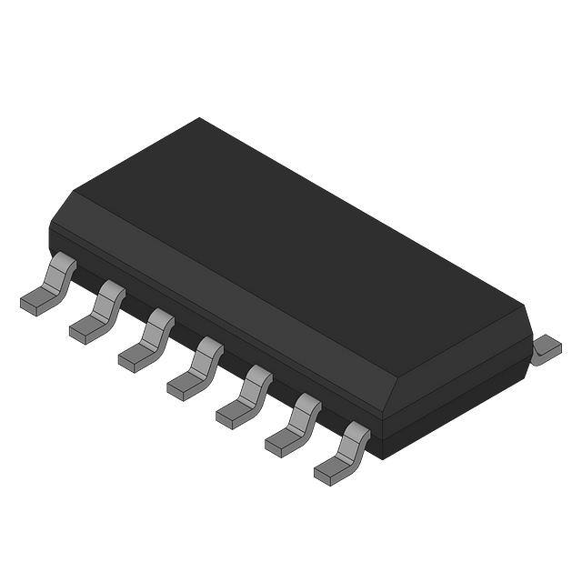
PG-SSOP-14
Analog Dimming feature to adjust average LED current
Internal 5 V Low Drop Out Voltage Regulator
Open Circuit Detection
Short to GND Protection
Output Overvoltage Protection
Internal Soft Start
Over Temperature Shutdown
Wide LED current range via simple adaptation of external components
300mV High Side Current Sense to ensure highest flexibility and LED current accuracy
Available in a small thermally enhanced PG-SSOP-14 package
Green Product (RoHS) Compliant
Description
The ILD1151 is a Multitopology High Power DC/DC Controller IC with built in protection features. The main
function of this device is to regulate a constant LED current. The constant current regulation is especially beneficial
for LED color accuracy and longer lifetime. The controller concept of the ILD1151 allows multiple configurations
such as Boost, Buck, Buck-Boost, SEPIC and Flyback by simply adjusting the external components. The ILD1151
offers the most flexible dimming options. Dimming can be achieved with analog or PWM input.The switching
frequency is adjustable in the range of 100 kHz to 500 kHz and can be synchronized to an external clock source.
The ILD1151 features an enable function reducing the shut-down current consumption to Iq_OFF < 10 µA. The
current mode regulation scheme of this device provides a stable regulation loop maintained by small external
compensation components. The integrated soft start feature limits the current peak as well as voltage overshoot
at start-up. This IC provides output overvoltage protection, device overtemperature shutdown and short circuit to
GND protection.
Type
Package
Marking
ILD1151
PG-SSOP-14
ILD1151
Datasheet
3
Rev. 1.1, 2012-04-11
�ILD1151
Overview
Applications
•
•
•
•
•
LED Controller for Industrial Applications
Universal Constant Current and Voltage Source
General Illumination e.g. Halogen Replacement
Residential Architectural and Industrial Commercial Lighting for in- and outdoor
Signal and Marker Lights for Orientation or Navigation (e.g. steps, exit ways, etc.)
For automotive and transportation applications, please refer to the Infineon® Auto LED products.
Datasheet
4
Rev. 1.1, 2012-04-11
�ILD1151
Block Diagram
2
Block Diagram
IN
14
LDO
13
2
SWO
4
SWCS
3
SGND
9
OVFB
6
FBH
7
FBL
5
PWMO
EN_INT/
PWM_INT
On/Off
Logic
Power Switch
Gate Driver
Soft
Start
Oscillator
FREQ / SYNC
IVCC
Power On
Reset
Internal
Supply
EN / PWMI
1
11
Slope
Comp.
PWM
Generator
Switch Current
Error Amplifier
Thermal
Protection
Leading Edge
Blanking
Open Load
+ Short to GND detection
Over Volage
Protection
SET
10
COMP
8
Reference
Current
Generation
Feedback Voltage
Error Amplifier
EN_INT/
PWM_INT
Dimming Switch
Gate Driver
12
GND
Figure 1
Datasheet
Block Diagram
5
Rev. 1.1, 2012-04-11
�ILD1151
Pin Configuration
3
Pin Configuration
3.1
Pin Assignment
IVCC
1
14
IN
SWO
2
13
EN/PWMI
SGND
3
12
GND
SWCS
4
11
FREQ/SYNC
PWMO
5
10
SET
FBH
6
9
OVFB
FBL
7
8
COMP
exposed
Pad
Figure 2
Pin Configuration
3.2
Pin Definitions and Functions
Pin
Symbol
Function
1
IVCC
Internal LDO Output;
Used for internal biasing and gate drive. Bypass with external capacitor close to
the pin. Pin must not be left open.
2
SWO
Switch Output;
Connect to gate of external switching MOSFET
3
SGND
Current Sense Ground;
Ground return for current sense switch
4
SWCS
Current Sense Input;
Detects the peak current through switch
5
PWMO
PWM Dimming Output;
Connect to gate of external MOSFET
6
FBH
Voltage Feedback Positive;
Non inverting Input (+)
7
FBL
Voltage Feedback Negative;
Inverting Input (-)
8
COMP
Compensation Input;
Connect R and C network to pin for stability
Datasheet
6
Rev. 1.1, 2012-04-11
�ILD1151
Pin Configuration
Pin
Symbol
Function
9
OVFB
Output Overvoltage Protection Feedback;
Connect to resistive voltage divider to set overvoltage threshold.
10
SET
Analog Dimming Input;
Load current adjustment Pin. Pin must not be left open. If analog dimming feature
is not used connect to IVCC pin.
11
FREQ / SYNC
Frequency Select or Synchronization Input;
Connect external resistor to GND to set frequency.
Or apply external clock signal for synchronization within frequency capture range.
12
GND
Ground;
Connect to system ground.
13
EN / PWMI
Enable or PWM Input;
Apply logic HIGH signal to enable device or PWM signal for dimming LED.
14
IN
Supply Input;
Supply for internal biasing.
EP
Datasheet
Exposed Pad;
Connect to external heatspreading GND Cu area (e.g. inner GND layer of
multilayer PCB with thermal vias).
7
Rev. 1.1, 2012-04-11
�ILD1151
General Product Characteristics
4
General Product Characteristics
4.1
Absolute Maximum Ratings
Absolute Maximum Ratings1)
Tj = -40 °C to +125 °C; all voltages with respect to ground, positive current flowing into pin
(unless otherwise specified)
Pos.
Parameter
Symbol
Limit Values
Min.
Max.
Unit Conditions
Voltages
4.1.1
IN
Supply Input
VIN
-0.3
45
V
–
4.1.2
EN / PWMI
Enable or PWM Input
VEN
-40
45
V
–
4.1.3
FBH-FBL
Feedback Error Amplifier Differential
VFBH-VFBL
-40
61
V
The maximum delta
must not exceed 61V
4.1.4
FBH
Feedback Error Amplifier Positive Input
VFBH
-40
61
V
The difference between
VFBH and VFBL must not
exceed 61V, refer to
Parameter 4.1.3
4.1.5
FBL
VFBL
Feedback Error Amplifier Negative Input
-40
61
V
The difference between
VFBH and VFBL must not
exceed 61V, refer to
Parameter 4.1.3
4.1.6
FBH and FBL current
IFBL,FBH
–
1
mA
t < 100ms,
VFBH - VFBL = 0.3V
4.1.7
OVFB
Over Voltage Feedback Input
VOVP
SWCS
Switch Current Sense Input
VSWCS
SWO
Switch Gate Drive Output
VSWO
4.1.13
SGND
Current Sense Switch GND
4.1.14
-0.3
5.5
V
–
-0.3
6.2
V
t < 10s
-0.3
5.5
V
–
-0.3
6.2
V
t < 10s
-0.3
5.5
V
–
-0.3
6.2
V
t < 10s
VSGND
-0.3
0.3
V
–
COMP
Compensation Input
VCOMP
-0.3
5.5
V
–
-0.3
6.2
V
t < 10s
FREQ / SYNC; Frequency and
Synchronization Input
VFREQ / SYNC -0.3
5.5
V
–
VPWMO
4.1.19
PWMO
PWM Dimming Output
4.1.20
SET
4.1.21
IVCC
Internal Linear Voltage Regulator Output
VSET
VIVCC
4.1.8
4.1.9
4.1.10
4.1.11
4.1.12
4.1.15
4.1.16
4.1.17
4.1.18
4.1.22
-0.3
6.2
V
t < 10s
-0.3
5.5
V
–
-0.3
6.2
V
t < 10s
-0.3
45
V
–
-0.3
5.5
V
–
-0.3
6.2
V
t < 10s
-40
150
°C
–
Temperatures
4.1.23
Junction Temperature
Datasheet
Tj
8
Rev. 1.1, 2012-04-11
�ILD1151
General Product Characteristics
Absolute Maximum Ratings1)
Tj = -40 °C to +125 °C; all voltages with respect to ground, positive current flowing into pin
(unless otherwise specified)
Pos.
4.1.24
Parameter
Symbol
Storage Temperature
Limit Values
Unit Conditions
Min.
Max.
Tstg
-55
150
°C
–
VESD,HBM
VESD,HBM
-2
2
kV
HBM2)
-4
4
kV
HBM2)
ESD Susceptibility
4.1.25
ESD Resistivity of all Pins
4.1.26
ESD Resistivity of IN, EN/PWMI, FBH,
FBL and SET pin to GND
1) Not subject to production test, specified by design.
2) ESD susceptibility, Human Body Model “HBM” according to ANSI/ESDA/JEDEC JS-001 (1.5kΩ, 100pF)
Note: Stresses above the ones listed here may cause permanent damage to the device. Exposure to absolute
maximum rating conditions for extended periods may affect device reliability.
Note: Integrated protection functions are designed to prevent IC destruction under fault conditions described in the
data sheet. Fault conditions are considered as “outside” normal operating range. Protection functions are
not designed for continuous repetitive operation.
4.2
Pos.
Functional Range
Parameter
4.2.1
Supply Voltage Range
4.2.2
Feedback Voltage Input
4.2.3
Junction Temperature
Symbol
VIN
VFBH;
VFBL
Tj
Limit Values
Unit
Conditions
Min.
Max.
4.5
451)
V
VIVCC > VIVCC,RTH,d
3
60
V
–
-40
125
°C
–
1) Not subject to production test, specified by design.
Note: Within the functional range the IC operates as described in the circuit description. The electrical
characteristics are specified within the conditions given in the related electrical characteristics table.
Datasheet
9
Rev. 1.1, 2012-04-11
�ILD1151
General Product Characteristics
4.3
Thermal Resistance
Note: This thermal data was generated in accordance with JEDEC JESD51 standards. For more information, go
to www.jedec.org.
Pos.
Parameter
4.3.1 Junction to Case
Symbol
1) 2)
4.3.2 Junction to Ambient
4.3.3
4.3.4
1) 3)
RthJC
RthJA
RthJA
RthJA
Limit Values
Unit
Conditions
–
Min.
Typ.
Max.
–
10
–
K/W
–
47
–
K/W
2s2p
–
54
–
K/W
1s0p + 600 mm2
–
64
–
K/W
1s0p + 300 mm2
1) Not subject to production test, specified by design.
2) Specified RthJC value is simulated at natural convection on a cold plate setup (all pins and the exposed pad are fixed to
ambient temperature). Ta=25°C; The IC is dissipating 1W.
3) Specified RthJA value is according to JEDEC 2s2p (JESD 51-7) + (JESD 51-5) and JEDEC 1s0p (JESD 51-3) + heatsink
area at natural convection on FR4 board; The device was simulated on a 76.2 x 114.3 x 1.5 mm board. The 2s2p board
has 2 outer copper layers (2 x 70µm Cu) and 2 inner copper layers (2 x 35µm Cu). A thermal via (diameter = 0.3 mm and
25 µm plating) array was applied under the exposed pad and connected the first outer layer (top) to the first inner layer and
second outer layer (bottom) of the JEDEC PCB. Ta=25°C; The IC is dissipating 1W.
Datasheet
10
Rev. 1.1, 2012-04-11
�ILD1151
Switching Regulator
5
Switching Regulator
5.1
Description
The ILD1151 regulator is suitable for Boost, Buck, Buck-Boost, SEPIC and Flyback configurations. The constant
output current is especially useful for light emitting diode (LED) applications. The regulator function is implemented
by a pulse width modulated (PWM) current mode controller.
The PWM current mode controller uses the peak current through the external power switch and error in the output
current to determine the appropriate pulse width duty cycle (on time) for constant output current. The current mode
controller provides a PWM signal to an internal gate driver which then outputs to an external n-channel
enhancement mode metal oxide field effect transistor (MOSFET) power switch.
The current mode controller also has built-in slope compensation to prevent sub-harmonic oscillations which is a
characteristic of current mode controllers operating at high duty cycles (>50% duty).
An additional built-in feature is an integrated soft start that limits the current through the inductor and external
power switch during initialization. The soft start function gradually increases the inductor and switch current over
tSS (Parameter 5.2.8) to minimize potential overvoltage at the output.
OV FB
H when
OVFB >1.25V
OVFB 9
VRef =
1.25V
High when
IVCC < 4.0V
COMP 8
FBH 6
x1
EA
FBL 7
OFF
when H
I EA
0 if SET < 1.6V
SET 10
0
VRef
Low when
T j > 175 °C
1
V
= VRef
Figure 3
Datasheet
R
&
Output Stage
OFF when
Low
R
Slope Comp
S
t
Clock
&
Q
INV
1
Q
S
I
&
Gate Driver
Supply
&
Q
Q
2 SWO
Current
Sense
PWM-FF
Error-FF
1 IVCC
Gate
Driver
0.3V
Oscillator
FREQ/
11
SYNC
Soft start
>
1
I SL O PE
(SET − 0.1V )
5
= VRef
4.0V
NOR
Current
Comp High when
l EA - I SLOPE - I CS > 0
gmEA
UV IVCC
NAND 2
&
I CS
4 SWCS
3 SGND
Switching Regulator Block Diagram
11
Rev. 1.1, 2012-04-11
�ILD1151
Switching Regulator
5.2
Electrical Characteristics
All parameters have been tested at 25°C, unless otherwise specified.
1)
Table 1
EC Switching Regulator
VIN = 24V; Tj = -40 °C to +125 °C, all voltages with respect to ground, positive current flowing into pin; (unless
otherwise specified)
Pos.
Parameter
Symbol
Limit Values
Min.
Typ.
Max.
Unit
Conditions
Regulator:
5.2.1
Feedback Reference Voltage
VREF
0.29
0.30
0.31
V
refer to Figure 29
VREF= VFBH -VFBL
VSET= 5V
ILED= 350 mA
5.2.2
Feedback Reference Voltage
VREF
0.057
0.06
0.063
V
refer to Figure 29
VREF= VFBH -VFBL
VSET= 0.4V
ILED= 70mA
5.2.3
Feedback Reference Voltage
Offset
VREF_offset –
–
5
mV
5.2.4
Voltage Load Regulation
(ΔVREF /
VREF) /
ΔIBO
–
–
5
%/A
5.2.5
Switch Peak Over Current
Threshold
VSWCS
130
150
170
mV
refer to Figure 17
and Figure 29
VREF= VFBH -VFBL
VSET= 0.1V
VOUT>VIN
refer to Figure 29
VSET = 5V;
ILED = 100 to 500mA
VFBH = VFBL = 5V
VCOMP = 3.5V
5.2.6
Maximum Duty Cycle
93
95
%
Fixed frequency mode
5.2.7
Maximum Duty Cycle
–
–
%
Synchronization mode
5.2.8
Soft Start Ramp
DMAX,fixed 91
DMAX,sync 88
tSS
350
1000
1500
µs
VFB rising from 5% to
95% of VFB, typ.
5.2.9
IFBH
Feedback High Input Current
IFBH
38
46
54
µA
VFBH - VFBL = 0.3V
5.2.10
IFBL
Feedback Low Input Current
IFBL
15
21
27
µA
VFBH - VFBL = 0.3V
5.2.11
Switch Current Sense Input
Current
ISWCS
10
50
100
µA
VSWCS = 150mV
5.2.12
Input Undervoltage Shutdown
3.5
–
4.5
V
5.2.13
Input Voltage Startup
VIN,off
VIN,on
–
–
4.85
V
VIN decreasing
VIN increasing
1) Not subject to production test, specified by design
Datasheet
12
Rev. 1.1, 2012-04-11
�ILD1151
Switching Regulator
Table 1
EC Switching Regulator
VIN = 24V; Tj = -40 °C to +125 °C, all voltages with respect to ground, positive current flowing into pin; (unless
otherwise specified)
Pos.
Parameter
Symbol
Limit Values
Min.
Typ.
Max.
Unit
Conditions
Gate Driver for external Switch
5.2.14
Gate Driver Peak Sourcing
Current
ISWO,SRC
–
380
–
mA
1)
VSWO = 1V to 4V
5.2.15
Gate Driver Peak Sinking
Current
ISWO,SNK
–
550
–
mA
1)
VSWO = 4V to 1V
5.2.16
Gate Driver Output Rise Time
tR,SWO
–
30
60
ns
1)
5.2.17
Gate Driver Output Fall Time
tF,SWO
–
20
40
ns
5.2.18
Gate Driver Output Voltage
VSWO
4.5
–
5.5
V
CL,SWO = 3.3nF;
VSWO = 1V to 4V
1)
CL,SWO = 3.3nF;
VSWO = 4V to 1V
1)
CL,SWO = 3.3nF;
1) Not subject to production test, specified by design
Datasheet
13
Rev. 1.1, 2012-04-11
�ILD1151
Oscillator and Synchronization
6
Oscillator and Synchronization
6.1
Description
The internal oscillator is used to determine the switching frequency of the boost regulator. The switching frequency
can be selected from 100 kHz to 500 kHz with an external resistor to GND. To set the switching frequency with an
external resistor the following formula can be applied.
R FREQ =
1
(141 × 10 [ ])× ( f
− 12
s
Ω
FREQ
[1s ])
(
) [Ω ]
− 3 . 5 × 10 3 [Ω ]
In addition, the oscillator is capable of changing from the frequency set by the external resistor to a synchronized
frequency from an external clock source. If an external clock source is provided on the pin FREQ/SYNC, then the
internal oscillator synchronizes to this external clock frequency and the boost regulator switches at the
synchronized frequency. The synchronization frequency capture range is 250 kHz to 500 kHz.
Oscillator
FREQ / SYNC
11
VCLK
Figure 4
Clock Frequency
Detector
RFREQ
PWM
Logic
Multiplexer
Gate
Driver
2
SWO
Oscillator and Synchronization Block Diagram and Simplified Application Circuit
TSYNC = 1 / fSYNC
VSYNC
tSYNC,TR
tSYNC,TR
tSYNC,PWH
4.5 V
VSYNC,H
VSYNC,L
0.5 V
t
Figure 5
Datasheet
Synchronization Timing Diagram
14
Rev. 1.1, 2012-04-11
�ILD1151
Oscillator and Synchronization
6.2
Electrical Characteristics
All parameters have been tested at 25°C, unless otherwise specified.
Table 2
EC Oscillator and Synchronization
VIN = 24V; Tj = -40 °C to +125 °C, all voltages with respect to ground, positive current flowing into pin; (unless
otherwise specified)
Pos.
Parameter
Symbol
Limit Values
Min.
Typ.
Max.
Unit
Conditions
RFREQ = 20kΩ
Oscillator:
fFREQ
fFREQ
250
300
350
kHz
100
–
500
kHz
FREQ / SYNC Supply
Current
IFREQ
–
–
-700
µA
VFREQ = 0V
Frequency Voltage
VFREQ
1.16
1.24
1.32
V
fFREQ = 100kHz
6.2.1
Oscillator Frequency
6.2.2
Oscillator Frequency
Adjustment Range
6.2.3
6.2.4
Synchronization
6.2.5
Synchronization Frequency
Capture Range
fSYNC
250
–
500
kHz
–
6.2.6
Synchronization Signal
High Logic Level Valid
VSYNC,H
3.0
–
–
V
1) 2)
6.2.7
Synchronization Signal
Low Logic Level Valid
VSYNC,L
–
–
0.8
V
1) 2)
6.2.8
Synchronization Signal
Logic High Pulse Width
tSYNC,PWH 200
–
–
ns
1) 2)
1) Synchronization of external PWM ON signal to falling edge
2) Not subject to production test, specified by design
Datasheet
15
Rev. 1.1, 2012-04-11
�ILD1151
Oscillator and Synchronization
Typical Performance Characteristics of Oscillator
Switching Frequency fSW versus
Frequency Select Resistor to GND RFREQ/SYNC
600
500
fFREQ [kHz]
400
T j = 25 °C
300
200
100
0
0
10 20
30
40 50
60 70
80
RFREQ/SYNC [kohm]
Datasheet
16
Rev. 1.1, 2012-04-11
�ILD1151
Enable and Dimming Function
7
Enable and Dimming Function
7.1
Description
The enable function powers ON or OFF the device. A valid logic LOW signal on enable pin EN/PWMI powers OFF
the device and current consumption is less than Iq_OFF (Parameter 7.2.14). A valid logic HIGH enable signal on
enable pin EN/PWMI powers on the device. The enable function features an integrated pull down resistor which
ensures that the IC is shut down and the power switch is OFF in case the enable pin EN is left open.
In addition to the enable function described above, the EN/PWMI pin detects a pulse width modulated (PWM) input
signal that is fed through to an internal gate driver. The internal gate driver outputs the same PWM signal on the
PWMO pin to an external N-channel enhancement mode MOSFET for PWM dimming an LED load. PWM dimming
an LED is a commonly practiced dimming method and can prevent color shift in an LED light source. Moreover
the PWM output function may also be used to drive other types of loads besides LED.
The enable and PWM input function share the same pin. Therefore a valid logic LOW signal at the EN/PWMI pin
needs to differentiate between an enable power OFF or an PWM dimming LOW signal. The device differentiates
between enable OFF and PWM dimming signal by requiring the enable OFF at the EN/PWMI pin to stay LOW for
the Enable Turn OFF Delay Time (tEN,OFF,DEL Parameter 7.2.6).
IN
14
Enable
Microcontroller
EN / PWMI
13
Enable / PWMI
Logic
LDO
Enable
Gate
Driver
PWMI
Figure 6
Datasheet
1
2
Gate
Driver
5
IVCC
SWO
PWMO
Block Diagram and Simplified Application Circuit Enable and LED Dimming
17
Rev. 1.1, 2012-04-11
�ILD1151
Enable and Dimming Function
tEN,START
TPWMI
tPWMI,H
tEN,OFF,DEL
VEN/PWMI
VEN/PWMI,ON
VEN/PWMI,OFF
t
VIVCC
VIVCC,ON
VIVCC,RTH
t
VPWMO
TFREQ =
VSWO
t
1
fFREQ
t
Power ON
Normal
Dim
Normal
Dim
Normal
SWO ON
PWMO OFF
SWO ON
PWMO OFF
SWO ON
PWMO ON
SWO OFF
PWMO ON
SWO OFF
PWMO ON
Figure 7
Timing Diagram Enable and LED Dimming
7.2
Electrical Characteristics
Power OFF Delay Time
Power OFF
Iq_OFF
All parameters have been tested at 25°C, unless otherwise specified.
Table 3
EC Enable and Dimming
VIN = 24V; Tj = -40 °C to +125 °C, all voltages with respect to ground, positive current flowing into pin; (unless
otherwise specified)
Pos.
Parameter
Symbol
Limit Values
Min.
Typ.
3.0
–
Unit
Conditions
V
–
V
–
Max.
Enable/PWM Input:
7.2.1
Enable/PWMI
Turn On Threshold
VEN/PWMI,ON
7.2.2
Enable/PWMI
Turn Off Threshold
VEN/PWMI,OFF –
Datasheet
–
18
0.8
Rev. 1.1, 2012-04-11
�ILD1151
Enable and Dimming Function
Table 3
EC Enable and Dimming
VIN = 24V; Tj = -40 °C to +125 °C, all voltages with respect to ground, positive current flowing into pin; (unless
otherwise specified)
Pos.
Parameter
Symbol
Limit Values
Min.
Unit
Conditions
Typ.
Max.
VEN/PWMI,HYS 50
IEN/PWMI,H
–
200
400
mV
1)
–
30
µA
VEN/PWMI = 16.0V
7.2.3
Enable/PWMI Hysteresis
7.2.4
Enable/PWMI
High Input Current
7.2.5
Enable/PWMI
Low Input Current
IEN/PWMI,L
–
0.1
1
µA
VEN/PWMI = 0.5V
7.2.6
Enable Turn Off
Delay Time
tEN,OFF,DEL
8
10
12
ms
–
7.2.7
PWMI Min Duty Time
4
–
–
µs
–
7.2.8
Enable Startup Time
tPWMI,H
tEN,START
100
–
–
µs
1)
Gate Driver for Dimming Switch:
7.2.9
PWMO Gate Driver Peak
Sourcing Current
IPWMO,SRC
–
230
–
mA
1)
VPWMO = 1V to 4V
7.2.10
PWMO Gate Driver Peak
Sinking Current
IPWMO,SNK
–
370
–
mA
1)
VPWMO = 4V to 1V
7.2.11
PWMO Gate Driver
Output Rise Time
tR,PWMO
–
50
100
ns
1)
CL,PWMO = 3.3nF;
7.2.12
PWMO Gate Driver
Output Fall Time
tF,PWMO
–
30
60
ns
7.2.13
PWMO Gate Driver
Output Voltage
VPWMO
4.5
–
5.5
V
VPWMO = 1V to 4V
1)
CL,PWMO = 3.3nF;
VPWMO = 4V to 1V
1)
CL,PWMO = 3.3nF;
Current Consumption
7.2.14
Current Consumption,
Shutdown Mode
Iq_OFF
–
–
10
µA
7.2.15
Current Consumption,
Active Mode2)
Iq_ON
–
–
7
mA
VEN/PWMI = 0.8 V;
Tj ≤ 105C; VIN = 16V
VEN/PWMI ≥ 4.75V;
IBO = 0mA;
VSWO = 0% Duty Cycle
1) Not subject to production test, specified by design
2) Dependency on switching frequency and gate charge of boost and dimming switch.
Datasheet
19
Rev. 1.1, 2012-04-11
�ILD1151
Linear Regulator
8
Linear Regulator
8.1
Description
The internal linear voltage regulator supplies the internal gate drivers with a typical voltage of 5V and current up
to ILIM,min (Parameter 8.2.2). An external output capacitor with ESR lower than RIVCC,ESR (Parameter 8.2.5) is
required on pin IVCC for stability and buffering transient load currents. During normal operation the external boost
and dimming MOSFET switches will draw transient currents from the linear regulator and its output capacitor.
Proper sizing of the output capacitor must be considered to supply sufficient peak current to the gate of the
external MOSFET switches.
Integrated undervoltage protection for the external switching MOSFET:
An integrated undervoltage reset threshold circuit monitors the linear regulator output voltage (VIVCC) and resets
the device in case the output voltage falls below the IVCC Undervoltage Reset switch OFF Threshold (VIVCC,RTH,d
Parameter 8.2.7). The Undervoltage Reset threshold for the IVCC pin helps to protect the external switches from
excessive power dissipation by ensuring the gate drive voltage is sufficient to enhance the gate of an external logic
level N-channel MOSFET.
IN
14
1
IVCC
Linear Regulator
EN / PWMI
Figure 8
Datasheet
13
Gate
Drivers
Voltage Regulator Block Diagram and Simplified Application Circuit
20
Rev. 1.1, 2012-04-11
�ILD1151
Linear Regulator
8.2
Electrical Characteristics
All parameters have been tested at 25°C, unless otherwise specified.
Table 4
EC Line Regulator
VIN = 24V; Tj = -40 °C to +125 °C, all voltages with respect to ground, positive current flowing into pin; (unless
otherwise specified)
Pos.
Parameter
Symbol
Limit Values
Min.
Typ.
Max.
Unit
Conditions
8.2.1
Output Voltage
VIVCC
4.85
5
5.15
V
6V ≤ VIN ≤ 45V
0.1mA ≤ IIVCC ≤ 50mA
8.2.2
Output Current Limitation
ILIM
51
–
90
mA
8.2.3
Drop out Voltage
VDR
–
–
0.5
V
VIN = 13.5V
VIVCC = 4.5V
VIN = 4.5V
IIVCC = 25mA
8.2.4
CIVCC
0.47
IVCC Buffer Capacitor ESR
RIVCC,ESR –
Undervoltage Reset Headroom VIVCC,HDRM 100
1
100
µF
1) 2)
–
0.5
Ω
1)
–
–
mV
8.2.5
IVCC Buffer Capacitor
8.2.7
IVCC Undervoltage Reset
switch OFF Threshold
VIVCC,RTH,d 3.6
–
4.0
V
VIVCC decreasing
VIVCC - VIVCC,RTH,d
3)
VIVCC decreasing.
8.2.8
IVCC Undervoltage Reset
switch ON Threshold
VIVCC,RTH,i
–
4.5
V
VIVCC increasing
8.2.6
–
1) Not subject to production test, specified by design
2) Minimum value given is needed for regulator stability; application might need higher capacitance than the minimum.
3) Selection of external switching MOSFET is crucial and the VIVCC,RTH,d min. as worst case VGS must be considered.
Datasheet
21
Rev. 1.1, 2012-04-11
�ILD1151
Protection and Diagnostic Functions
9
Protection and Diagnostic Functions
9.1
Description
The ILD1151 has integrated circuits to diagnose and protect against output overvoltage, open load, open feedback
and overtemperature faults. Additionally the FBH and FBL potential is monitored and in case the LED load short
circuits to GND (see description Figure 15) the regulator stops the operation and protects the system. In case any
of the six fault conditions occur the PWMO and IVCC signal will change to an active logic LOW signal to
communicate that a fault has occurred (detailed overview in Figure 9 and Figure 10 below). Figure 11 illustrates
the various open load and open feedback conditions. In case of an overtemperature condition the integrated
thermal shutdown function turns off the gate drivers and internal linear voltage regulator. The typical junction
shutdown temperature is 175°C (Tj,SD Parameter 9.2.2). After cooling down the IC will automatically restart.
Thermal shutdown is an integrated protection function designed to prevent IC destruction and is not intended for
continuous use in normal operation (Figure 13). To calculate the proper overvoltage protection resistor values an
example is given in Figure 14.
Input
Protection and
Diagnostic Circuit
Output
Output
Overvoltage
Open Load
OR
SWO and PWMO
Gate Driver Off
Short to GND
Open Feedback
Overtemperature
Linear Regualtor
Off
OR
Input
Undervoltage
Figure 9
Datasheet
Protection and Diagnostic Function Block Diagram
22
Rev. 1.1, 2012-04-11
�ILD1151
Protection and Diagnostic Functions
Input
Condition
Overvoltage @
Output
Level*
False
True
False
True
False
True
False
True
False
True
False
True
Open Load
Short to GND @ LED
chain
Open Feedback
Overtemperature
Undervoltage @
Input
SWO
Sw*
L
Sw*
L
Sw*
L
Sw*
L
Sw*
L
Sw*
L
Output
PWMO
IVCC
H or Sw *
Active
L
Active
H or Sw *
Active
L
Active
H or Sw *
Active
L
Active
H or Sw *
Active
L
Active
H or Sw *
Active
L
Shutdown
H or Sw *
Active
L
Shutdown
*Note:
Sw = Switching
False = Condition does not exist
True = Condition does exist
Diagnosis Truth Table
VBO
Open Circuit 3
Open Circuit 1
ROVH
OVFB
Open Circuit 2
9
VOVFB,TH
D1
ROVL
D2
Open Circuit
Condition
Fault Condition
Fault Threshold Voltage
VREF
1
Open FBH
-20 to -100 mV
2
Open FBL
0.5 to 1.0 V
3
Open VBO
-20 to -100 mV
4
Open PWMO
Detected by overvoltage
D3
Feedback Voltage
Error Amplifier
FBH
FBL
VREF
D4
6
7
D5
+
VREF
-
D6
Max Threshold = 1.0 V
D7
D8
Min Threshold = 0.5 V
D9
D10
Typical V REF = 0.3 V
Open Circuit 4
TDIM
PWMO
Figure 11
Datasheet
Open FBL
Overvoltage
Compartor
RFB
Output Open Circuit Conditions
Max Threshold = -20 mV
Min Threshold = -100 mV
5
Open FBH
Open VBO
Figure 10
Open Load and Open Feedback Conditions
23
Rev. 1.1, 2012-04-11
�ILD1151
Protection and Diagnostic Functions
Startup
Normal
VIVCC
Thermal
Shutdown
Overvoltage
Open Load /
Feedback
1
2
3
Shutdown
VIVCC,RTH,i
VIVCC,RTH,d
Tj
t
Tj,SD,HYST
1
Tj,SD
VBO
VOVFB,HYS
t
2
VOVFB ≥ VOVFB,TH
VIN
3
VFBH-VFBL
t
VREF,2
tSS
tSS
0.3 V Typ
t
VREF,1
VPWMO
t
Figure 12
Datasheet
Open load, Overvoltage and Overtemperature Timing Diagram
24
Rev. 1.1, 2012-04-11
�ILD1151
Protection and Diagnostic Functions
VEN/PWMI
H
L
t
Tj
TjSD
ΔΤ
TjSO
t
Ta
VSWO
t
ILED
Ipeak
t
VPWMO
t
VIVCC
5V
t
Device
OFF
Figure 13
Datasheet
Normal Operation
Overtemp
Fault
ON
Overtemp
ON
Fault
Overtemp
ON
Fault
Overtemp
Fault
Device overtemperature protection behavior
25
Rev. 1.1, 2012-04-11
�ILD1151
Protection and Diagnostic Functions
VOVFB
example: VOUT,max=40V
VOVP,max
1.25mA
OVFB
Overvoltage Protection
ACTIVE
40V
≅ 33.2kΩ
1.25mA
ROVH
VOVFB,TH
9
ROVL
GND
1kΩ 1.25V
1.25V
Overvoltage Protection is
disabled
12
t
Figure 14
Overvoltage Protection description
Short to GND protection for Highside Return Applications (B2B) from Figure 23
The FBH and FBL pins features a Short to GND detection threshold (VFBL,FBH_S2G). If the potential on those pins is
below this threshold the Device stops his operation. This means that the PWMO signal changes to inactive state
(LOW potential) and the corresponding p-channel (TDIM2) is switched OFF accordingly and protects the LED chain.
For the B2B application some external components are needed to ensure a LOW potential during a short circuit
event. D1 and D2 are low power diodes (BAS16-03W) and the resistor Rlim (10kOhm) is needed to limit the current
through this path. The diode D3 should be a high power diode and is needed to protect the RFB and the FBH and
FBL pins in case of an short circuit to GND event. This short circuit detection and protection concept considers
potential faults for LED chains (LED Modules) which are separated from the ECU via two wires (at the beginning
and at the end of the LED chain). If the short circuit condition disappears, the device will re-start with a soft start.
CBO
Vbb
wire
harness
RFB
CIN
VFBL,FBH
D2
D1 Rlim
LED Module
Dn
D3
60V
Short to GND
wire
harness
TDIM2
D1
Normal Operation
Short to GND
LBO
TDIM1
DBO ILED
ISW
PWMO
TSW
SWO
SWCS
FBH
FBL
IN
Figure 15
Datasheet
VOUT
4.5V
VFBL,FBH_S2G
SGND
Device working with parameter
deviations
Short Circuit detected on
FBH/FBL
t
Short Circuit to GND Protection
26
Rev. 1.1, 2012-04-11
�ILD1151
Protection and Diagnostic Functions
9.2
Electrical Characteristics
All parameters have been tested at 25°C, unless otherwise specified.
Table 5
EC Protection and Diagnosis
VIN = 24V; Tj = -40 °C to +125 °C, all voltages with respect to ground, positive current flowing into pin; (unless
otherwise specified)
Pos.
Parameter
Symbol
Limit Values
Min.
Typ.
Max.
–
2
Unit
Conditions
Short Circuit Protection
9.2.1
FBH and FBL Short-Circuit fault VFBL,FBH_S2G 1.5
sensing common mode range
V
refer to Figure 15
VFBH=VFBL
decreasing
Temperature Protection:
9.2.2
Over Temperature Shutdown
9.2.3
Over Temperature Shutdown
Hystereses
Tj,SD
Tj,SD,HYST
160
175
190
°C
1)
–
15
–
°C
1)
refer to Figure 13
Overvoltage Protection:
9.2.4
Output Over Voltage Feedback
Threshold Increasing
VOVFB,TH
1.21
1.25
1.29
V
refer to Figure 14
9.2.5
Output Over Voltage Feedback
Hysteresis
VOVFB,HYS
50
–
150
mV
1)
9.2.6
Over Voltage Reaction Time
tOVPRR
2
–
10
µs
Output Voltage
decreasing
9.2.7
Over Voltage Feedback Input
Current
IOVFB
-1
0.1
1
µA
VOVFB = 1.25V
Output Voltage
decreasing
Open Load and Open Feedback Diagnostics
9.2.8
Open Load/Feedback
Threshold
VREF,1,3
-100
–
-20
mV
refer to Figure 11
VREF = VFBH - VFBL
Open Circuit 1 or 3
9.2.9
Open Feedback Threshold
VREF,2
0.5
–
1
V
VREF = VFBH - VFBL
Open Circuit 2
1) Specified by design; not subject to production test.
Note: Integrated protection functions are designed to prevent IC destruction under fault conditions described in the
data sheet. Fault conditions are considered as “outside” normal operating range. Protection functions are
not designed for continuous repetitive operation.
Datasheet
27
Rev. 1.1, 2012-04-11
�ILD1151
Analog Dimming
10
Analog Dimming
This pin is influencing the Feedback Voltage Error Amplifier by generating an internal current accordingly to an
external reference voltage (VSET). If the analog dimming feature is not needed this pin must be connected to IVCC
or external > 1.6V supply. Different application scenarios are described in Figure 18. This pin can also go outside
of the ECU for instance if a thermistor is connected on a separated LED Module and the Analog Dimming Input is
used to thermally protect the LEDs. For reverse battery protection of this pin an external series resistor should be
placed to limit the current.
10.1
Purpose of Analog Dimming:
1) It is difficult for LED manufacturers to deliver LEDs which have the same Brightness, Colorpoint and Forward
Voltage Class. Due to this relatively wide spread of the crucial LED parameters customers order LEDs from one
or maximum two different colorpoint classes. The LED manufacturer must preselect the LEDs to deliver the
requested colorpoint class. Those preselected LEDs are matched in terms of the colorpoint but a variation of the
brightness remains. To correct the brightness deviation an analog dimming feature is needed. The mean LED
current can be adjusted by applying an external voltage VSET at the SET pin.
2) If the DC/DC application is separated from the LED loads the ECU manufacturers aim is to develop one
hardware which should be able to handle different load current conditions (e.g. 80mA to 400mA) to cover different
applications. To achieve this average LED current adjustment the analog dimming is a crucial feature.
10.2
Description
Application Example:
Desired LED current = 400mA. For the calculation of the correct Feedback Resistor RFB the following equation can
be used: This formula is valid if the analog dimming feature is disabled and VSET > 1.6V.
I LED =
V
VREF
0.3V
--> RFB = REF --> R
= 750mΩ
FB =
I LED
RFB
400mA
A decrease of the average LED current can be achieved by controlling the voltage at the SET pin (VSET) between
0V and 1.6V. The mathematical relation is given in the formula below:
I
LED
=
V
− 0 ,1 V
5 * R FB
SET
If VSET is 100mV the LED current is only determined by the internal offset voltages of the comparators. For this
example ILED = 0A if VSET < 100mV. Refer to the concept drawing in Figure 17.
Datasheet
28
Rev. 1.1, 2012-04-11
�ILD1151
Analog Dimming
VREF
[V]
typ. 300mV
[V]
Analog Dimming
Disabled
Analog Dimming Feature Enabled
V − 0.1V
I LED = SET
5 * RFB
Figure 16
VSET
1.6V
100 mV
I LED =
VREF
RFB
Voltage VSET versus LED current
VREF
VOUT
RFB
ILED
FBL
FBH
7
6
IFBL
IFBH
R2
R1
Vint
VBandgap = 1.6V
VREF_offset
+
+
+
-
-
Feedback Voltage
Error Amplifier
ISET
SET
10
VSET
ISET
n*ISET
R3
100mV
COMP
GND
8
12
CCOMP
RCOMP
Figure 17
Datasheet
Concept Drawing Analog Dimming
29
Rev. 1.1, 2012-04-11
�ILD1151
Analog Dimming
Multi-purpose usage of the Analog dimming feature
1) A µC integrated digital analog converter (DAC) output or a stand alone DAC can be used to supply the SET pin
of the ILD1151. The integrated voltage Regulator (VIVCC) can be used to supply the µC or external components if
the current consumption does not exceed 25mA.
2) The analog dimming feature is directly connected to the input voltage of the system. In this configuration the
LED current is reduced if the input voltage VIN is decreasing. The DC/DC boost converter is changing (increasing)
the switching duty cycle if VIN drops to a lower potential. This is causing an increase of the input current
consumption. If applications require a decrease of the LED current in respect to VIN variations this setup can be
choosen.
3) The usage of an external resistor divider connected between IVCC (integrated 5V regulator output and gate
buffer pin) SET and GND can be choosen for systems without µC on board. The concept allows to control the LED
current via placing cheap low power resistors. Furthermore a temperature sensitive resistor (Thermistor) to protect
the LED loads from thermal destruction can be connected additionally.
4) If the analog dimming feature is not needed the SET pin must be connected directly to >1.6V potential (e.g.
IVCC potential)
5) Instead of an DAC the µC can provide a PWM signal and an external R-C filter is producing a constant voltage
for the analog dimming. The voltage level is depending on the PWM frequency (fPWM) and duty cycle (DC) which
can be controlled by the µc software after reading the coding resistor placed at the LED module.
Datasheet
30
Rev. 1.1, 2012-04-11
�ILD1151
Analog Dimming
.
+5V
1
2
CIVCC
D/A-Output
µC
10
Vbb
1
14
IVCC
IN
RSET2
SET
10
SET
VSET
VSET RSET1
GND
Cfilter
GND
12
12
3
4
VIVCC = +5V
1
RSET2
Rfilter
CIVCC
10
VSET RSET1
VIVCC = +5V
IVCC
GND
VSET ~ VIVCC
12
IVCC
10
SET
CIVCC
SET
Cfilter
1
Cfilter
GND
12
5
+5V
1
IVCC
10
SET
CIVCC
PWM
PWM output
Rfilter
µC
(e.g. XC866)
Cfilter
VSET
GND
12
Figure 18
Datasheet
Analog Dimming in various applications
31
Rev. 1.1, 2012-04-11
�ILD1151
Analog Dimming
10.3
Electrical Characteristics
All parameters have been tested at 25°C, unless otherwise specified.
Table 6
EC Analog Dimming
VIN = 24V; Tj = -40 °C to +125 °C, all voltages with respect to ground, positive current flowing into pin; (unless
otherwise specified)
Pos.
Parameter
Symbol
Limit Values
Min.
Typ.
Max.
0
–
1.6
Unit
Conditions
V
1)
Analog Dimming Range
10.3.1
SET programming range
VSET
refer to Figure 16
1) Specified by design; not subject to production test.
Datasheet
32
Rev. 1.1, 2012-04-11
�ILD1151
Application Information
11
Application Information
Note: The following information is given as a hint for the implementation of the device only and shall not be
regarded as a description or warranty of a certain functionality, condition or quality of the device.
LBO
VIN
VIN = 4.5V to 45V
DBO
CIN
TDIM2
CBO
S
DZ
IN
TSW
SWO
2
SWCS
4
RFB
RCS
PWM
IC2
Microcontroller
(e.g. XC866)
VSET
10
Rfilter
SET
IC1
ILD1151
Cfilter
PWMI
Digital Dimming
13
EN / PWMI
Spread
STATUS Spectrum
11
FREQ / SYNC
8
COMP
SGND
3
OVFB
9
VREF
RDIM1
VCC or VIVCC
Analog Dimming
ILED
G
RDIM2
14
D
R OVH
Short
to
GND
R OVL
FBH
IVCC
1
D4
D5
R POL
DPOL
D6
D7
FBL
7
D8
PWMO
PWMO
RCOMP
D2
D3
6
CIVCC
CCOMP
R FREQ
D1
TDIM1
5
D9
GND
D10
12
LED load
seperated via wire
harness
Figure 19
Boost to Ground Application Circuit - B2G + Short Circuit protection (Boost configuration)
Reference
Designator
Value
Manufacturer
Part
Number
Type
Quantity
D1 - 10
White
Osram
LUW H9GP
LED
10
DBO
Schottky , 3 A, 100 VR
Vishay
SS3H10
Diode
1
DZ
5V or 10V
Vishay
ZENER
Diode
1
DPOL
80V Diode
Infineon
BAS1603W
Diode
1
CIN, CBO
100 uF, 50V
Panasonic
EEEFK1H101GP
Capacitor
2
CCOMP
10 nF
EPCOS
X7R
Capacitor
1
CIVCC
1uF , 6.3V
EPCOS
MLCC CCNPZC105KBW X7R
Capacitor
1
IC1
--
Infineon
ILD1151
IC
1
IC2
--
Infineon
XC866
IC
1
LBO
100 uH
Coilcraft
MSS1278T-104ML
Inductor
1
RDIM1+2, RCOMP ,
RPOL
10 kΩ, 1%
Panasonic
ERJ3EKF1002V
Resistor
4
RFB
820 mΩ, 1%
Panasonic
ERJ14BQFR82U
Resistor
1
RFREQ
20 kΩ, 1%
Panasonic
ERJ3EKF2002V
Resistor
1
ROVH
33.2 kΩ, 1%
Panasonic
ERJ3EKF3322V
Resistor
1
ROVL
1 kΩ, 1%
Panasonic
ERJ3EKF1001V
Resistor
1
RCS
50 mΩ, 1%
Panasonic
ERJB1CFR05U
Resistor
1
TSW
100V N-ch, 35A
Infineon
IPG20N10S4L-22
Transistor
1
TDIM 1, TDIM2
60V Dual N-ch (3.1A) and
P-ch. enh. (2A)
Infineon
BSO615CG
Transistor
1
alternativ: 100V N-ch (0.37A),
Infineon
BSP123
Transistor
1
alternativ: 60V P-ch (1.9A)
Infineon
BSP171P
Transistor
1
Figure 20
Datasheet
Bill of Materials for B2G Application Circuit
33
Rev. 1.1, 2012-04-11
�ILD1151
Application Information
L1
DBO
CSEPIC
VIN
VIN = 4.5V to 45V
CIN
ISW
RFB
L2
14
IN
TSW
SWO
2
SWCS
4
VREF
CBO
ILED
RCS
VCC or VIVCC
PWM
VSET
Analog Dimming
10
Rfilter
IC2
Microcontroller
(e.g. XC866)
SET
SGND
3
OVFB
9
D2
D3
IC1
ILD1151
Cfilter
PWMI
Digital Dimming
13
EN / PWMI
Spread
STATUS Spectrum
11
FREQ / SYNC
8
COMP
D1
R OVH
R OVL
D4
D5
D6
Number of LEDs could be
variable independent from VIN:
Æ BUCK-BOOST operation
D7
FBH
6
FBL
7
IVCC
1
CCOMP
DPOL
RPOL
Dn
C IVCC
RFREQ
RCOMP
PWMO
PWMO
TDIM
5
GND
12
Figure 21
SEPIC Application Circuit (Buck-Boost configuration)
Reference
Designator
Value
Manufacturer
Part
Number
D1 - n
White
Osram
DBO
Schottky, 3 A, 100 VR
Vishay
Type
Quantity
LUW H9GP
LED
variable
SS3H10
Diode
1
DPOL
80V Diode
Infineon
BAS1603W
Diode
1
CSEPIC
3.3 uF, 20V
EPCOS
X7R, Low ESR
Capacitor
1
CIN , CBO
100 uF, 50V
Panasonic
EEEFK1H101GP
Capacitor
2
CCOMP
10 nF
EPCOS
X7R
Capacitor
1
CIVCC
1uF , 6.3V
EPCOS
X7R
Capacitor
1
IC1
--
Infineon
ILD1151
IC
1
IC2
--
Infineon
XC866
IC
1
L1 , L2
47 uH
Coilcraft
MSS1278T-473ML
Inductor
2
alternativ: 22uH coupled
inductor
Coilcraft
MSD1278-223MLD
Inductor
1
RCOMP, RPOL
10 kΩ, 1%
Panasonic
ERJ3EKF1002V
Resistor
2
RFB
820 mΩ, 1%
Panasonic
ERJ14BQFR82U
Resistor
1
RFREQ
20 kΩ, 1%
Panasonic
ERJ3EKF2002V
Resistor
1
ROVH
33.2 kΩ, 1%
Panasonic
ERJ3EKF3322V
Resistor
1
ROVL
1 kΩ, 1%
Panasonic
ERJ3EKF1001V
Resistor
1
RCS
50 mΩ, 1%
Panasonic
ERJB1CFR05U
Resistor
1
TDIM,TSW
Dual N-ch enh. (60V, 20A)
Infineon
IPG20N06S4L-26
Transistor
1
alternativ: 100V N-ch, 35A
Infineon
IPD35N10S3L-26
Transistor
2
alternativ : 60V N-ch, 2.6A
Infineon
BSP318S
Transistor
2
Figure 22
Datasheet
Bill of Materials for SEPIC Application Circuit
34
Rev. 1.1, 2012-04-11
�ILD1151
Application Information
DBO
VIN
VIN = 4.5V to 45V
L1
CIN
ISW
RFB
L2
14
IN
TSW
SWO
2
SWCS
4
VREF
CBO
ILED
RCS
VCC or VIVCC
PWM
VSET
Analog Dimming
10
Rfilter
IC2
Microcontroller
(e.g. XC866)
SET
3
OVFB
9
ROVH
PWMI
13
EN / PWMI
Output
11
FREQ / SYNC
8
COMP
D1
D2
IC1
ILD1151
Cfilter
Digital Dimming
STATUS
SGND
D3
ROVL
D4
D5
D6
FBH
6
FBL
7
IVCC
1
Number of LEDs could be
variable independent from VIN:
Æ BUCK-BOOST operation
D7
CCOMP
DPOL
RPOL
Dn
CIVCC
RFREQ
RCOMP
PWMO
PWMO
12
Figure 23
TDIM
5
GND
Flyback Application Circuit (Buck-Boost configuration)
Reference
Designator
Value
Manufacturer
Part
Number
Type
Quantity
D1 - n
White
Osram
LUW H9GP
LED
variable
DBO
Schottky, 3 A, 100 VR
Vishay
SS3H10
Diode
1
CBO
3.3 uF, 50V (100V)
EPCOS
X7R, Low ESR
Capacitor
1
CIN
100 uF, 50V
Panasonic
EEEFK1H101GP
Capacitor
1
CCOMP
47 nF
EPCOS
X7R
Capacitor
1
CIVCC
1 uF , 6.3V
EPCOS
X7R
Capacitor
1
IC1
--
Infineon
ILD1151
IC
1
IC2
--
Infineon
XC866
IC
1
L1 , L2
1 µH / 9 uH
EPCOS
Transformer EHP 16
Inductor
1
RCOMP, RPOL
10 kΩ, 1%
Panasonic
ERJ3EKF1002V
Resistor
2
DPOL
80 V Diode
Infineon
BAS1603W
Diode
1
RFB
820 mΩ, 1%
Isabellenhütte
SMS – Power Resistor
Resistor
1
RFREQ
10 kΩ, 1%
Panasonic
ERJ3EKF1002V
Resistor
1
ROVH
56.2 kΩ, 1%
Panasonic
ERJ3EKF5622V
Resistor
1
ROVL
1.24 kΩ, 1%
Panasonic
ERJ3EKF1241V
Resistor
1
RCS
5 mΩ, 1%
Isabellenhütte
SMS - Power Resistor
Resistor
1
TDIM,TSW
Dual N-ch enh. (60V, 20A)
Infineon
IPG20N06S4L-26
Transistor
1
alternativ: 100V N-ch, 35A
Infineon
IPG20N10S4L-22
Transistor
2
alternativ : 60V N-ch, 2.6A
Infineon
BSP318S
Transistor
2
Figure 24
Datasheet
Bill of Materials for Flyback Application Circuit
35
Rev. 1.1, 2012-04-11
�ILD1151
Application Information
C BO
DSC1:
Low Power Diode
Rlim:10kΩ
range
DSC2:
Low Power Diode
RFB
TDIM2
VIN = 4.5V to 45V
CIN
D3
Power
Schottky
Diode
Dn
DZ
D1
Short to GND
Short to GND
RDIM1
LBO
DBO
TDIM1
VOUT
5
VCC or V IVCC
PWM
Analog Dimming
STATUS
PWMO
6
FBH
7
FBL
14
IN
10
SET
VSET
Rfilter
I LED
I SW
PWMO
IC2
Microcontroller
(e.g. XC866)
RDIM2
Number of LEDs could be variable!
Æ BUCK-BOOST configfuration
SWO
2
SWCS
4
SGND
3
OVFB
9
TSW
RCS
ROVH
IC1
ILD1151
Cfilter
PWMI
Digital Dimming
13
EN / PWMI
Spread Spectrum
11
FREQ / SYNC
ROVL
COMP
8
IVCC
1
CCOMP
CIVCC
GND
RFREQ
Figure 25
RCOMP
12
Boost to Battery Application Circuit - B2B + Short Circuit protection (Buck-Boost config.)
Reference
Designator
Value
Manufacturer
Part
Number
Type
Quantity
D1 - n
White
Osram
LUW H9GP
Diode
variable
DBO , D3
Schottky, 3 A, 100 VR
Vishay
SS3H10
Diode
2
DSC1 , DSC2
Low Power Diode
Infineon
BAS16-03W
Diode
2
DZ
Zener Diode
--
--
Diode
1
CBO
100 uF, 80V
Panasonic
EEVFK1K101Q
Capacitor
1
CIN
100 uF, 50V
Panasonic
EEEFK1H101GP
Capacitor
1
CCOMP
10 nF
EPCOS
X7R
Capacitor
1
CIVCC
1 uF, 6.3V
EPCOS
MLCC CCNPZC105KBW X7R
Capacitor
1
IC1
--
Infineon
ILD1151
IC
1
IC2
--
Infineon
XC866
IC
1
LBO
100 uH
Coilcraft
MSS1278T-104ML_
Inductor
1
RCOMP , RDIM1, RDIM2, Rlim
10 kΩ, 1%
Panasonic
ERJ3EKF1002V
Resistor
4
RFB
820 mΩ, 1%
Panasonic
ERJ14BQFR82U
Resistor
1
RFREQ
20 kΩ, 1%
Panasonic
ERJ3EKF2002V
Resistor
1
ROVH
33.2 kΩ, 1%
Panasonic
ERJP06F5102V
Resistor
1
ROVL
1 kΩ, 1%
Panasonic
ERJ3EKF1001V
Resistor
1
RCS
50 mΩ, 1%
Panasonic
ERJB1CFR05U
Resistor
1
TDIM1,TDIM2
60V Dual N-ch (3.1A) and P-ch. enh. (2A)
Infineon
BSO615CG
Transistor
1
alternativ: 100V N-ch (0.37A),
Infineon
BSP123
Transistor
1
alternativ: 60V P-ch (1.9A)
Infineon
BSP171P
Transistor
1
N-ch, OptiMOS-T2 100V, 35A
Infineon
IPD35N10S3L-26
Applicationdrawing _plus_BOM_B2B_IL
Transistor
1
D1151 _April2012 .vsd
alternativ: 60V N-ch, 30A
Infineon
IPD30N06S4L-23
Transistor
1
alternativ : 60V N-ch, 2.6A
Infineon
BSP318S
Transistor
1
TSW
Figure 26
Datasheet
Bill of Materials for B2B Application Circuit
36
Rev. 1.1, 2012-04-11
�ILD1151
Application Information
D BO
D1
C BO
TDIM2
VIN = 4.5V to 45V
C IN
14
S
DZ
RDIM2
BUCK Setup:
VIN > VOUT
PWMO
PWM
Rfilter
IC1
ILD1151
PWMI
Digital Dimming
13
Spread Spectrum
STATUS
EN / PWMI
11
FREQ / SYNC
8
COMP
R FREQ
LBO
RFB
FBH
6
FBL
7
IVCC
1
R COMP
TDIM1
C IVCC
R POL
R POL
TSW
SWO
SWCS
2
SGND
3
OVFB
9
4
RCS
C COMP
PWMO
5
SET
C filter
IC2
Microcontroller
(e.g. XC866)
PWMO
VSET
10
VREF
RDIM1
IN
VCC or VIVCC
Analog Dimming
D2
ILED
GND
12
Figure 27
Buck Application Circuit + Short Circuit protection
Reference
Designator
Value
Manufacturer
Part
Number
Type
Quantity
D1 -2
White
Osram
LE UW Q9WP
LED
2
DBO
Schottky, 3 A, 100 VR
Vishay
SS3H10
Diode
1
DZ
10V
Vishay
Zener Diode
Diode
1
DPOL
80V Diode
Infineon
BAS1603W
Diode
1
CBO
4.7 uF, 50V
EPCOS
X7R
Capacitor
1
CIN
100 uF, 50V
Panasonic
EEEFK 1H101GP
Capacitor
1
CCOMP
47 nF
EPCOS
X7R
Capacitor
1
CIVCC
1 uF , 6.3V
EPCOS
MLCC CCNPZC105KBW X7R
Capacitor
1
IC1
--
Infineon
ILD1151
IC
1
IC2
--
Infineon
XC866
IC
1
L1
22 µH
Coilcraft
MSS1278T
Inductor
1
RDIM1+2, RCOMP,
RPOL
10 kΩ, 1%
Panasonic
ERJ3EKF1002V
Resistor
4
RFB
820 mΩ, 1%
Isabellenhütte
SMS – Power Resistor
Resistor
1
RFREQ
20 kΩ, 1%
Panasonic
ERJ3EKF2002V
Resistor
1
RCS
50 mΩ, 1%
Isabellenhütte
SMS - Power Resistor
Resistor
1
TDIM1
60V, 0.28A
Infineon
BSS138
Transistor
1
TDIM2
-60V, -1.9A
Infineon
BSP171
Transistor
1
TSW
30V, 22A
Infineon
IPB22N03S4L-15
Transistor
1
alternativ : 60V N-ch, 2.6A
Infineon
BSP318S
Transistor
1
Figure 28
Datasheet
Bill of Materials for Buck Application Circuit
37
Rev. 1.1, 2012-04-11
�ILD1151
Application Information
I BO
VIN
VIN = 4.5V to 45V
LBO
DBO
CIN
ILoad
VBO
CBO
ISW
constant
VOUT
RL
14
CIVCC
1
SWO
2
SWCS
4
TSW
IN
IVCC
RCS
VCC or V IVCC
SGND
3
OVFB
9
ROVH
PWM
Analog Dimming
10
Rfilter
IC2
Microcontroller
(e.g. XC866)
Cfilter
SET
VSET
Digital Dimming
Output
IC1
ILD1151
5
PWMO
13
EN / PWMI
11
FREQ / SYNC
8
COMP
RFB 1
FBH
FBL
RCOMP
6
RFB2
C COMP
R FREQ
ROVL
VREF
7
RFB 3
GND
12
Figure 29
Boost Voltage Application Circuit
Reference
Designator
Value
Manufacturer
Part
Number
Type
Quantity
DBO
Schottky, 3 A, 100 VR
Vishay
SS3H10
Diode
1
CBO
100 uF, 80V
Panasonic
EEVFK1K101Q
Capacitor
1
CIN
100 uF, 50V
Panasonic
EEEFK1H101GP
Capacitor
1
CCOMP
10 nF
TBD
TBD
Capacitor
1
CIVCC
1 uF, 6.3V
Panasonic
MLCC CCNPZC105KBW X7R
Capacitor
1
IC1
--
Infineon
ILD1151
IC
1
IC2
--
Infineon
XC886
IC
1
LBO
100 uH
Coilcraft
MSS1278T-104ML_
Inductor
1
RCOMP
10 kΩ
TBD
TBD
Resistor
1
RFB1,RFB3
51 kΩ, 1%
Panasonic
ERJ3EKF5102V
Resistor
1
RFB2
1 kΩ, 1%
Panasonic
ERJ3EKF1001V
Resistor
1
RFREQ
20 kΩ, 1%
Panasonic
ERJ3EKF2002V
Resistor
2
ROVH
51 kΩ, 1%
Panasonic
ERJP06F5102V
Resistor
1
ROVL
1 kΩ, 1%
Panasonic
ERJ3EKF1001V
Resistor
1
RCS
50 mΩ, 1%
Panasonic
ERJB1CFR05U
Resistor
1
TSW
N-ch, 75 V, 65 mΩ
Infineon
IPD22N08S2L-50
Transistor
1
Figure 30
Bill of Materials for Boost Voltage Application Circuit
Note: This is a very simplified example of an application circuit. The function must be verified in the real application.
Datasheet
38
Rev. 1.1, 2012-04-11
�ILD1151
Application Information
11.1
•
•
Further Application Information
For further information you may contact http://www.infineon.com/
Application Note: ILD1150 / ILD1151 DC-DC Multitopology Controller IC for Industrial Applications
“Dimensioning and Stability Guideline - Theory and Practice”
Datasheet
39
Rev. 1.1, 2012-04-11
�ILD1151
Package Outlines
12
Package Outlines
0.19 +0.06
0.08 C
0.15 M C A-B D 14x
0.64 ±0.25
1
8
1
7
0.2
M
D 8x
Bottom View
3 ±0.2
A
14
6 ±0.2
D
Exposed
Diepad
B
0.1 C A-B 2x
14
7
8
2.65 ±0.2
0.25 ±0.05 2)
0.1 C D
8˚ MAX.
C
0.65
3.9 ±0.11)
1.7 MAX.
Stand Off
(1.45)
0 ... 0.1
0.35 x 45˚
4.9 ±0.11)
Index Marking
1) Does not include plastic or metal protrusion of 0.15 max. per side
2) Does not include dambar protrusion
PG-SSOP-14-1,-2,-3-PO V02
PG-SSOP-14
Figure 31
PG-SSOP-14
Green Product (RoHS compliant)
To meet the world-wide customer requirements for environmentally friendly products and to be compliant with
government regulations the device is available as a green product. Green products are RoHS-Compliant (i.e
Pb-free finish on leads and suitable for Pb-free soldering according to IPC/JEDEC J-STD-020).
For further package information, please visit our website:
http://www.infineon.com/packages.
Datasheet
40
Dimensions in mm
Rev. 1.1, 2012-04-11
�ILD1151
Revision History
13
Revision History
Revision
Date
Changes
1.0
2011-02-10
Initial Datasheet
1.1
2012-04-11
Page 3: RoHS Logo update
Page 3: Topology update
Application Information chapter update
Datasheet
41
Rev. 1.1, 2012-04-11
�Edition 2012-04-11
Published by
Infineon Technologies AG
81726 Munich, Germany
© 2012 Infineon Technologies AG
All Rights Reserved.
Legal Disclaimer
The information given in this document shall in no event be regarded as a guarantee of conditions or
characteristics. With respect to any examples or hints given herein, any typical values stated herein and/or any
information regarding the application of the device, Infineon Technologies hereby disclaims any and all warranties
and liabilities of any kind, including without limitation, warranties of non-infringement of intellectual property rights
of any third party.
Information
For further information on technology, delivery terms and conditions and prices, please contact the nearest
Infineon Technologies Office (www.infineon.com).
Warnings
Due to technical requirements, components may contain dangerous substances. For information on the types in
question, please contact the nearest Infineon Technologies Office.
Infineon Technologies components may be used in life-support devices or systems only with the express written
approval of Infineon Technologies, if a failure of such components can reasonably be expected to cause the failure
of that life-support device or system or to affect the safety or effectiveness of that device or system. Life support
devices or systems are intended to be implanted in the human body or to support and/or maintain and sustain
and/or protect human life. If they fail, it is reasonable to assume that the health of the user or other persons may
be endangered.
�