IM818-MCC Datasheet
CIPOS™ Maxi IM818
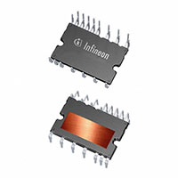
IM818-MCC
Description
The CIPOS™ Maxi IM818 product group offers the chance for integrating various power and control
components to increase reliability, optimize PCB size and system costs. It is designed to control three phase AC
motors and permanent magnet motors in variable speed drives applications such as low power motor drives (GPI,
Servo drives), pumps, fan drives and active filter for HVAC (Heating, Ventilation, and Air Conditioning). The
product concept is specially adapted to power applications, which need good thermal performance and
electrical isolation as well as EMI save control and overload protection.
Three phase inverter with 1200V TRENCHSTOP™ IGBTs and Emitter Controlled diodes are combined with an
optimized 6-channel SOI gate driver for excellent electrical performance.
Features
• Fully isolated Dual In-Line molded module
• 1200V TRENCHSTOP™ IGBT4
• Rugged 1200V SOI gate driver technology with stability
against transient and negative voltage
• Allowable negative VS potential up to -11 V
for signal transmission at VBS = 15 V
• Integrated bootstrap functionality
• Over current shutdown
• Built-in NTC thermistor for temperature monitor
• Under-voltage lockout at all channels
• Low side emitter pins accessible for phase
current monitoring (open emitter)
• Anti cross-conduction
• All of 6 switches turn off during protection
• Programmable fault clear timing and enable input
• Lead-free terminal plating; RoHS compliant
Potential applications
Fan drives and active filter for HVAC, pumps, and low power motor drives (GPI, Servo Drives)
Product validation
Qualified for industrial applications according to the relevant tests of JEDEC47/20/22.
Table 1
Product Information
Product Name
Package Type
IM818-MCC
DIP 36x23D
Datasheet
www.infineon.com
Standard Pack
Form
MOQ
14 pcs / tube
280
Please read the Important Notice and Warnings at the end of this document
page 1 of 21
Remark
V 2.3
2022-02-23
�CIPOS™ Maxi IM818
IM818-MCC
Table of Contents
Table of Contents
Description .................................................................................................................................... 1
Features ........................................................................................................................................ 1
Potential applications ..................................................................................................................... 1
Product validation .......................................................................................................................... 1
Table of Contents ........................................................................................................................... 2
1
Internal Electrical Schematic ................................................................................................... 3
2
2.1
2.2
Pin Configuration ................................................................................................................... 4
Pin Assignment ........................................................................................................................................ 4
Pin Description ........................................................................................................................................ 5
3
3.1
3.2
3.3
Absolute Maximum Ratings ..................................................................................................... 7
Module Section ........................................................................................................................................ 7
Inverter Section ....................................................................................................................................... 7
Control Section........................................................................................................................................ 7
4
Thermal Characteirstics .......................................................................................................... 8
5
Recommended Operation Conditions ....................................................................................... 9
6
6.1
6.2
Static Parameters ................................................................................................................. 10
Inverter Section ..................................................................................................................................... 10
Control Section...................................................................................................................................... 10
7
7.1
7.2
Dynamic Parameters ............................................................................................................. 11
Inverter Section ..................................................................................................................................... 11
Control Section...................................................................................................................................... 11
8
Thermistor Characteristics ..................................................................................................... 12
9
Mechanical Characteristics and Ratings ................................................................................... 13
10
Qualification Information....................................................................................................... 14
11
Diagrams and Tables ............................................................................................................. 15
11.1
TC Measurement Point ........................................................................................................................... 15
11.2
Backside Curvature Measurement Point .............................................................................................. 15
11.3
Switching Time Definition ..................................................................................................................... 16
12
Application Guide .................................................................................................................. 17
12.1
Typical Application Schematic ............................................................................................................. 17
12.2
Performance Charts .............................................................................................................................. 18
13
Package Outline .................................................................................................................... 19
Revision history............................................................................................................................. 20
Datasheet
2 of 21
V 2.3
2022-02-23
�CIPOS™ Maxi IM818
IM818-MCC
Internal Electrical Schematic
1
Internal Electrical Schematic
P (24)
(1) VS(U)
(2) VB(U)
VB1
HO1
RBS1
VS1
U (23)
(3) VS(V)
(4) VB(V)
VB2
RBS2
HO2
VS2
V (22)
(5) VS(W)
(6) VB(W)
VB3
RBS3
(7) HIN(U)
HIN1
(8) HIN(V)
HIN2
(9) HIN(W)
HIN3
(10) LIN(U)
LIN1
(11) LIN(V)
LIN2
(12) LIN(W)
LIN3
(13) VDD
VDD
(14) RFE
RFE
(15) ITRIP
ITRIP
(16) VSS
VSS
HO3
VS3
W (21)
LO1
NU (20)
LO2
NV (19)
LO3
NW (18)
(17) VTH
Thermistor
Figure 1
Datasheet
Internal electrical schematic
3 of 21
V 2.3
2022-02-23
�CIPOS™ Maxi IM818
IM818-MCC
Pin Configuration
2
Pin Configuration
2.1
Pin Assignment
Bottom view
(24) P
(1) VS(U)
(2) VB(U)
(3) VS(V)
(4) VB(V)
(23) U
(5) VS(W)
(6) VB(W)
(22) V
(7) HIN(U)
(8) HIN(V)
(9) HIN(W)
(10) LIN(U)
(11) LIN(V)
(12) LIN(W)
(13) VDD
(14) RFE
(15) ITRIP
(16) VSS
(17) VTH
Figure 2
(21) W
(20) NU
(19) NV
(18) NW
Module pinout
Table 2
Pin Assignment
Pin Number
Pin name
Pin Description
1
VS(U)
U-phase high side floating IC supply offset voltage
2
VB(U)
U-phase high side floating IC supply voltage
3
VS(V)
V-phase high side floating IC supply offset voltage
4
VB(V)
V-phase high side floating IC supply voltage
5
VS(W)
W-phase high side floating IC supply offset voltage
6
VB(W)
W-phase high side floating IC supply voltage
7
HIN(U)
U-phase high side gate driver input
8
HIN(V)
V-phase high side gate driver input
9
HIN(W)
W-phase high side gate driver input
10
LIN(U)
U-phase low side gate driver input
11
LIN(V)
V-phase low side gate driver input
12
LIN(W)
W-phase low side gate driver input
13
VDD
Low side control supply
Datasheet
4 of 21
V 2.3
2022-02-23
�CIPOS™ Maxi IM818
IM818-MCC
Pin Configuration
Pin Number
Pin name
Pin Description
14
RFE
Programmable fault clear time, fault output, enable input
15
ITRIP
Over current shutdown input
16
VSS
Low side control negative supply
17
VTH
Thermistor
18
NW
W-phase low side emitter
19
NV
V-phase low side emitter
20
NU
U-phase low side emitter
21
W
Motor W-phase output
22
V
Motor V-phase output
23
U
Motor U-phase output
24
P
Positive bus input voltage
2.2
Pin Description
It is not recommended for proper work to provide
input pulse-width lower than 1 µs.
HIN (U, V, W) and LIN (U, V, W) (Low side and high
side control pins, Pin 7 - 12)
The integrated gate driver provides additionally a
shoot through prevention capability which avoids
the simultaneous on-state of two gate drivers of the
same leg (i.e. HO1 and LO1, HO2 and LO2, HO3 and
LO3). When two inputs of a same leg are activated,
only former activated one is activated so that the leg
is kept steadily in a safe state.
These pins are positive logic and they are
responsible for the control of the integrated IGBTs.
The schmitt-trigger input thresholds of them are
such to guarantee LSTTL and CMOS compatibility
down to 3.3 V controller outputs. Pull-down resistor
of about 5 k is internally provided to pre-bias
inputs during supply start-up. Input schmitt-trigger
and noise filter provide beneficial noise rejection to
short input pulses.
A minimum deadtime insertion of typically 360 ns is
also provided by driver IC, in order to reduce crossconduction of the external power switches.
The noise filter suppresses control pulses which are
below the filter time tFIL,IN. The filter acts according to
Figure 4.
RFE (Fault / Fault clear time / Enable, Pin 14)
The RFE pin conbines three functions in one pin:
programmable fault clear time by RC-network, faultout and enable input.
CIPOSTM
Schmitt-Trigger
HINx
LINx
5k
VSS
Figure 3
a)
The programmable fault-clear time can be adjusted
by RC network, which is external pull-up resistor and
capacitor. For example, typical value is about 1ms at
INPUT NOISE
FILTER
SWITCH LEVEL
VIH; VIL
1 MΩ and 2 nF.
Input pin structure
tFIL,IN
b)
The fault-out indicates a module failure in case of
under voltage at pin VDD or in case of triggered over
current detection at ITRIP.
tFIL,IN
HIN
LIN
HIN
LIN
The microcontroller can pull this pin low to disable
the IPM functionality. This is enable function.
high
HO
LO
Figure 4
Datasheet
low
HO
LO
Input filter timing diagram
5 of 21
V 2.3
2022-02-23
�CIPOS™ Maxi IM818
IM818-MCC
Pin Configuration
The IC shuts down all the gate drivers power outputs,
when the VDD supply voltage is below VDDUV- = 11.2 V.
This prevents the external power switches from
critically low gate voltage levels during on-state and
therefore from excessive power dissipation.
CIPOS
Bi-direction
Schmitt-Trigger
NOISE FILTER
RFE
VSS
Figure 5
1
RON,FLT
From ITRIP - Latch
From UV detection
VB (U, V, W) and VS (U, V, W) (High side supplies,
Pin 1 - 6)
Internal circuit at pin RFE
VB to VS is the high side supply voltage. The high side
circuit can float with respect to VSS following the
external high side power device emitter voltage.
VTH (Thermistor, Pin 17)
The VTH pin provides direct access to the NTC,
which is referenced to VSS. An external pull-up
resistor connected to +5 V ensures that the resulting
voltage can be directly connected to the
microcontroller.
Due to the low power consumption, the floating
driver stage is supplied by integrated bootstrap
circuit.
The under-voltage detection operates with a rising
supply threshold of typical VBSUV+ = 11.2 V and a
falling threshold of VBSUV- = 10.2 V.
ITRIP (Over current detection function, Pin 15)
IM818 provides an over current detection function
by connecting the ITRIP input with the IGBT
collector current feedback. The ITRIP comparator
threshold (typ. 0.5 V) is referenced to VSS ground. An
input noise filter (tITRIP = typ. 500 ns) prevents the
driver to detect false over-current events.
VS(U, V, W) provide a high robustness against
negative voltage in respect of VSS of -50 V transiently.
This ensures very stable designs even under rough
conditions.
NW, NV, NU (Low side emitter, Pin 18 - 20)
Over current detection generates a shutdown of all
outputs of the gate driver after the shutdown
propagation delay of typically 1µs.
The low side emitters are available for current
measurements of each phase leg. It is
recommended to keep the connection to pin VSS as
short as possible in order to avoid unnecessary
inductive voltage drops.
Fault-clear time is set to typical 1.1ms at RRCIN = 1 M
Ω and CRCIN = 2 nF.
W, V, U (High side emitter and low side collector,
Pin 21 - 23)
VDD, VSS (Low side control supply and
reference, Pin 13, 16)
These pins are motor U, V, W input pins.
VDD is the control supply and it provides power both
to input logic and to output power stage. Input logic
is referenced to VSS ground.
P (Positive bus input voltage, Pin 24)
The high side IGBTs are connected to the bus
voltage. It is noted that the bus voltage does not
exceed 900 V.
The under-voltage circuit enables the device to
operate at power on when a supply voltage of at
least a typical voltage of VDDUV+ = 12.2 V is present.
Datasheet
6 of 21
V 2.3
2022-02-23
�CIPOS™ Maxi IM818
IM818-MCC
Absolute Maximum Ratings
3
Absolute Maximum Ratings
(VDD = 15V and TJ = 25°C, if not stated otherwise)
3.1
Module Section
Description
Symbol
Storage temperature range
TSTG
Operating case temperature
TC
Operating junction temperature
TJ
Isolation test voltage
VISO
3.2
Refer to Figure 6
1min, RMS, f = 60Hz
Value
Unit
-40 ~ 125
°C
-40 ~ 125
°C
-40 ~150
°C
2500
V
Value
Unit
1200
V
Inverter Section
Description
Symbol
Max. blocking voltage
Condition
VCES/VRRM
DC link supply voltage of P-N
VPN
Applied between P-N
900
V
VPN(surge)
Applied between P-N
1000
V
TC = 25°C, TJ < 150°C
±16
TC = 80°C, TJ < 150°C
±10
TC = 25°C, tp < 1 ms
±20
A
67.5
W
10
µs
Value
Unit
VS
1200
V
Repetitive peak reverse voltage of
bootstrap diode
VRRM
1200
V
Module control supply voltage
VDD
-1 ~ 20
V
High side floating supply voltage
(VB reference to VS)
VBS
-1 ~ 20
V
Input voltage (LIN, HIN, ITRIP, RFE)
VIN
-1 ~ VDD + 0.3
V
DC link supply voltage (surge) of P-N
DC collector current
IC
Peak collector current
ICP
Power dissipation per IGBT
Ptot
Short circuit withstand time
1
3.3
tSC
VDC ≤ 800 V, TJ = 150°C
A
Control Section
Description
High Side offset voltage
1
Condition
Symbol
Condition
Allowed number of short circuits: < 1000; Time between short circuits: > 1 s.
Datasheet
7 of 21
V 2.3
2022-02-23
�CIPOS™ Maxi IM818
IM818-MCC
Thermal Characteirstics
4
Thermal Characteirstics
Description
Symbol
Condition
Value
Min.
Typ.
Max.
Unit
Single IGBT thermal
resistance, junction-case
RthJC
High side V-phase IGBT
-
-
1.85
K/W
Single diode thermal
resistance, junction-case
RthJC,D
High side V-phase diode
-
-
2.50
K/W
Datasheet
8 of 21
V 2.3
2022-02-23
�CIPOS™ Maxi IM818
IM818-MCC
Recommended Operation Conditions
5
Recommended Operation Conditions
All voltages are absolute voltages referenced to VSS -potential unless otherwise specified.
Description
Symbol
Value
Min.
Typ.
Max.
Unit
DC link supply voltage of P-N
VPN
350
600
800
V
Low side supply voltage
VDD
13.5
15
18.5
V
High side floating supply voltage (VB vs. VS)
VBS
12.5
-
18.5
V
Logic input voltages LIN, HIN, ITRIP, RFE
VIN
0
-
5
V
PWM carrier frequency
FPWM
-
-
20
kHz
External dead time between HIN & LIN
DT
0.5
-
-
µs
VCOMP
-5
-
5
V
PWIN(ON)
PWIN(OFF)
1
-
-
µs
ΔVBS,
ΔVDD
-1
-1
-
1
1
V/µs
Voltage between VSS - N (including surge)
Minimum input pulse width
Control supply variation
Datasheet
9 of 21
V 2.3
2022-02-23
�CIPOS™ Maxi IM818
IM818-MCC
Static Parameters
6
Static Parameters
(VDD = 15V and TJ = 25°C, if not stated otherwise)
6.1
Inverter Section
Description
Collector-Emitter saturation voltage
Collector-Emitter leakage current
Diode forward voltage
6.2
Symbol
Condition
Value
Unit
Min.
Typ.
Max.
VCE(sat)
IC = 10 A
TJ = 25°C
150°C
-
2.0
2.6
2.4
-
V
ICES
VCE = 1200 V
-
-
1
mA
VF
IF = 10 A
TJ = 25°C
150°C
-
1.75
1.75
2.25
-
V
Control Section
Description
Symbol
Condition
Value
Min.
Typ.
Max.
Unit
Logic "1" input voltage (LIN, HIN)
VIH
-
1.9
2.3
V
Logic "0" input voltage (LIN, HIN)
VIL
0.7
0.9
-
V
ITRIP positive going threshold
VIT,TH+
475
500
525
mV
ITRIP input hysteresis
VIT,HYS
-
55
-
mV
VDD and VBS supply under voltage
positive going threshold
VDDUV+
VBSUV+
11.5
10.5
12.2
11.2
13.0
12.0
V
VDD / VBS supply under voltage negative
going threshold
VDDUVVBSUV-
10.5
9.5
11.2
10.2
12.0
11.0
V
VDD / VBS supply under voltage lockout
hysteresis
VDDUVH
VBSUVH
-
1
-
V
Quiescent VBx supply current (VBx only)
IQBS
HIN = 0 V
-
175
-
µA
Quiescent VDD supply current (VDD only)
IQDD
LIN = 0 V, HINX = 5 V
-
1
-
mA
Input bias current for LIN, HIN
IIN+
VIN = 5 V
-
1
-
mA
IITRIP+
VITRIP = 5 V
-
30
100
µA
Input bias current for RFE
IRFE
VRFE = 5 V,
VITRIP = 0 V
-
-
5
µA
RFE output voltage
VRFE
IRFE = 10 mA,
VITRIP = 1 V
-
0.4
-
V
Input bias current for ITRIP
VRFE positive going threshold
VRFE,TH+
-
1.9
2.3
V
VRFE negative going threshold
VRFE,TH-
0.7
0.9
-
V
Bootstrap diode forward voltage
VF_BSD
IF = 0.3 mA
-
0.9
-
V
Bootstrap diode resistance
RBSD
Between VF = 4 V
and VF = 5 V
-
120
-
Ω
Datasheet
10 of 21
V 2.3
2022-02-23
�CIPOS™ Maxi IM818
IM818-MCC
Dynamic Parameters
7
Dynamic Parameters
(VDD = 15V and TJ = 25°C, if not stated otherwise)
7.1
Inverter Section
Description
Symbol
Turn-on propagation delay time
ton
Turn-on rise time
tr
Turn-on switching time
tc(on)
Reverse recovery time
trr
Turn-off propagation delay time
toff
Turn-off fall time
tf
Condition
VLIN, HIN = 5 V,
IC = 10 A,
VDC = 600 V
VLIN, HIN = 0 V,
IC = 10 A,
VDC = 600 V
Value
Typ.
Max.
-
800
-
ns
-
45
-
ns
-
230
-
ns
-
420
-
ns
-
960
-
ns
-
100
-
ns
-
200
-
ns
-
1200
-
ns
Turn-off switching time
tc(off)
Short circuit propagation delay time
tSCP
From VIT,TH+ to 10%
ISC
Eon
VDC = 600 V,
IC = 10 A
TJ = 25°C
150°C
-
1.1
1.6
-
Eoff
VDC = 600 V,
IC = 10 A
TJ = 25°C
150°C
-
0.6
0.9
-
Erec
VDC = 600 V,
IC = 10 A
TJ = 25°C
150°C
-
0.3
0.6
-
IGBT turn-on energy (includes
reverse recovery of diode)
IGBT turn-off energy
Diode recovery energy
7.2
Unit
Min.
mJ
mJ
mJ
Control Section
Description
Symbol
Condition
Value
Unit
Min.
Typ.
Max.
Input filter time ITRIP
tITRIP
VITRIP = 1 V
-
500
-
ns
Input filter time at LIN, HIN for
turn on and off
tFIL,IN
VLIN, HIN = 0 V or 5 V
-
350
-
ns
1.1
-
ms
-
650
900
ns
300
-
-
ns
-
-
130
ns
VITRIP = 1V,
Fault clear time after ITRIP-fault
tFLT,CLR
Vpull-up = 5V
(RRFE = 1 MΩ, CRFE = 2 nF)
ITRIP to Fault propagation delay
tFLT
Internal deadtime
DTIC
Matching propagation delay
time (On & Off) all channels
MT
Datasheet
VLIN, HIN = 0 or 5 V,
VITRIP = 1V
VIN = 0 or VIN = 5 V
External dead time > 500ns
11 of 21
V 2.3
2022-02-23
�CIPOS™ Maxi IM818
IM818-MCC
Thermistor Characteristics
8
Thermistor Characteristics
Description
Condition
Resistor
Symbol
Unit
Min.
Typ.
Max.
RNTC
-
85
-
kΩ
B (25/100)
-
4092
-
K
TNTC = 25°C
B-constant of NTC
(Negative Temperature Coefficient)
Value
3500
2500
2000
1500
30
Thermistor resistance [kΩ ]
Thermistor resistance [kΩ ]
35
3000
Min.
Typ.
Max.
25
20
15
10
5
0
50 55 60 65 70 75 80 85 90 95 100 105 110 115 120 125 130
1000
Thermistor temperature [℃]
500
0
-40 -30 -20 -10 0
Figure 6
10 20 30 40 50 60 70 80 90 100 110 120 130
Thermistor temperature [℃]
Thermistor resistance – temperature curve and table
(For more information, please refer to the application note ‘AN2019-16 CIPOS™ Maxi IM818 application note’)
Datasheet
12 of 21
V 2.3
2022-02-23
�CIPOS™ Maxi IM818
IM818-MCC
Mechanical Characteristics and Ratings
9
Mechanical Characteristics and Ratings
Description
Comparative Tracking Index (CTI)
Mounting torque
Backside Curvature
Weight
Datasheet
Condition
M3 screw and washer
Refer to Figure 8
13 of 21
Value
Min.
600
0.49
0
-
Typ.
7.1
Max.
0.78
150
-
Unit
Nm
µm
g
V 2.3
2022-02-23
�CIPOS™ Maxi IM818
IM818-MCC
Qualification Information
10
Qualification Information
UL Certification
File number E314539
Moisture sensitivity level
(SOP package only)
-
RoHS Compliant
Yes (Lead-free terminal plating)
ESD (Electrostatic
Discharge)
Datasheet
HBM (Human body model)
Class as per JESD22-A114
2 (>2000V to < 4000V)
CDM (Charged Device model)
Class as per JESD22-C101
C3 (>=1000V)
14 of 21
V 2.3
2022-02-23
�CIPOS™ Maxi IM818
IM818-MCC
Diagrams and Tables
11
Diagrams and Tables
11.1
TC Measurement Point
Figure 7
11.2
Figure 8
TC measurement point1
Backside Curvature Measurement Point
Backside curvature measurement position
Any measurement except for the specified point in Figure 7 is not relevant for the temperature verification and
brings wrong or different information.
1
Datasheet
15 of 21
V 2.3
2022-02-23
�CIPOS™ Maxi IM818
IM818-MCC
Diagrams and Tables
11.3
Switching Time Definition
HINx
LINx
2.1V
0.9V
trr
toff
ton
10%
iCx
90%
90%
tf
10%
tr
10%
10%
10%
vCEx
tc(on)
tc(off)
Figure 9
Datasheet
Switching times definition
16 of 21
V 2.3
2022-02-23
�CIPOS™ Maxi IM818
IM818-MCC
Application Guide
12
Application Guide
12.1
Typical Application Schematic
P (24)
(1) VS(U)
(2) VB(U)
HO1
VB1
RBS1
VS1
U (23)
(3) VS(V)
#4
(4) VB(V)
VB2
RBS2
HO2
VS2
V (22)
3-ph AC
Motor
(5) VS(W)
(6) VB(W)
VB3
RBS3
HO3
VS3
W (21)
#5
#1
(7) HIN(U)
(8) HIN(V)
(9) HIN(W)
(10) LIN(U)
(11) LIN(V)
Micro
Controller
HIN1
LO1
HIN2
NU (20)
HIN3
LIN1
LIN2
LO2
(12) LIN(W)
#6
LIN3
#7
NV (19)
(13) VDD
VDD line
(14) RFE
#2
(15) ITRIP
(16) VSS
(17) VT H
#3.2
Temperature monitor
RFE
ITRIP
LO3
NW (18)
VSS
Thermistor
#3.1
5 or
3.3V line
Control
GND line
5 or
3.3V line
Power
GND line
VDD
U-phase current sensing
V-phase current sensing
W-phase current sensing
Figure 10
Typical application circuit
1.
Input circuit
- To reduce input signal noise by high speed switching, the RIN and CIN filter circuit should be mounted. (100 Ω, 1 nF)
- CIN should be placed as close to VSS pin as possible.
2. Itrip circuit
- To prevent protection function errors, CITRIP should be placed as close to Itrip and VSS pins as possible.
3. RFE circuit
3.1 Pull-up resistor (RRFE) and pull-down capacitor (CRFE)
- RFE output is an open drain output. This signal line should be pulled up to the positive side of the 5 V / 3.3 V control
power supply voltage (VCTR) with a proper resistor RFE.
- The fault-clear time is adjusted by RC network of RRFE and CRFE and pull-up voltage.
4.
5.
6.
7.
◼ tFLTCLR = -RRFE ∙ CRFE ∙ ln(1- VRFE,TH+/VCTR) + internal fault-clear time 160 s
◼ tFLTCLR = -1 M x 2 nF x ln(1 - 1.9 / 5 V) + 160s 1.1ms at RRFE = 1 M, CRFE = 2 nF and VCTR = 5 V
◼ A pull-up resistor is limited to max. 2 M
◼ In case of VCTR is higher than 5 V, the RRFE needs to be at least 200 k to limit the IC power dissipation
3.2 RC filter
- It is recommended that RC filter be placed as close to the controller as possible.
VB-VS circuit
- Capacitor for high side floating supply voltage should be placed as close to VB and VS pins as possible.
Snubber capacitor
- The wiring between IM818 and snubber capacitor including shunt resistor should be as short as possible.
Shunt resistor
- The shunt resistor of SMD type should be used for reducing its stray inductance.
Ground pattern
- Ground pattern should be separated at only one point of shunt resistor as short as possible.
Datasheet
17 of 21
V 2.3
2022-02-23
�CIPOS™ Maxi IM818
IM818-MCC
Application Guide
12.2
Performance Charts
IM818-MCC
Maximum Output Current, IO [Arms]
10
9
8
7
FSW=5kHz
FSW=15kHz
6
5
4
3
VDC=600V, VDD=VBS=15V, SVPWM
2
TJ ≤150℃, TC ≤125oC, M.I.=0.8, P.F.=0.8
1
0
0
10
20
30
40
50
60
70
80
90
100
110
120
130
140
Case Temperature, TC [℃]
Figure 11
Maximum operating current SOA1
This maximum operating current SOA is just one of example based on typical characteristics for this product. It
can be changed by each user’s actual operating conditions.
1
Datasheet
18 of 21
V 2.3
2022-02-23
�CIPOS™ Maxi IM818
IM818-MCC
Package Outline
13
Datasheet
Package Outline
19 of 21
V 2.3
2022-02-23
�CIPOS™ Maxi IM818
IM818-MCC
Revision history
Revision history
Document
version
Date of release
Description of changes
2.0
2018-06-25
Initial release
2.1
2018-08-20
Minor change - Figure7, section 4(thermal resistance), section
10(qualification information), section 13(package outline)
2.2
2019-06-07
Corrected typo section 7.1(HINx, LINx = 0 V)
Minor change – Table 1 and reference document (AN) number in figure 6
2.3
2022-02-23
Update notes (3.1) in section 12.1
Datasheet
20 of 21
V 2.3
2022-02-23
�Trademarks
All referenced product or service names and trademarks are the property of their respective owners.
Edition 2022-02-23
Published by
Infineon Technologies AG
81726 München, Germany
© 2022 Infineon Technologies AG.
All Rights Reserved.
Do you have a question about this
document?
Email: erratum@infineon.com
Document reference
ifx1
IMPORTANT NOTICE
The information given in this document shall in no
event be regarded as a guarantee of conditions or
characteristics (“Beschaffenheitsgarantie”) .
With respect to any examples, hints or any typical
values stated herein and/or any information
regarding the application of the product, Infineon
Technologies hereby disclaims any and all
warranties and liabilities of any kind, including
without limitation warranties of non-infringement of
intellectual property rights of any third party.
In addition, any information given in this document
is subject to customer’s compliance with its
obligations stated in this document and any
applicable legal requirements, norms and standards
concerning customer’s products and any use of the
product of Infineon Technologies in customer’s
applications.
The data contained in this document is exclusively
intended for technically trained staff. It is the
responsibility of customer’s technical departments
to evaluate the suitability of the product for the
intended application and the completeness of the
product information given in this document with
respect to such application.
For further information on the product, technology,
delivery terms and conditions and prices please
contact your nearest Infineon Technologies office
(www.infineon.com).
Please note that this product is not qualified
according to the AEC Q100 or AEC Q101 documents
of the Automotive Electronics Council.
WARNINGS
Due to technical requirements products may contain
dangerous substances. For information on the types
in question please contact your nearest Infineon
Technologies office.
Except as otherwise explicitly approved by Infineon
Technologies in a written document signed by
authorized
representatives
of
Infineon
Technologies, Infineon Technologies’ products may
not be used in any applications where a failure of the
product or any consequences of the use thereof can
reasonably be expected to result in personal injury.
�