IPB033N10N5LF
MOSFET
OptiMOSTM�5�Linear�FET,�100�V
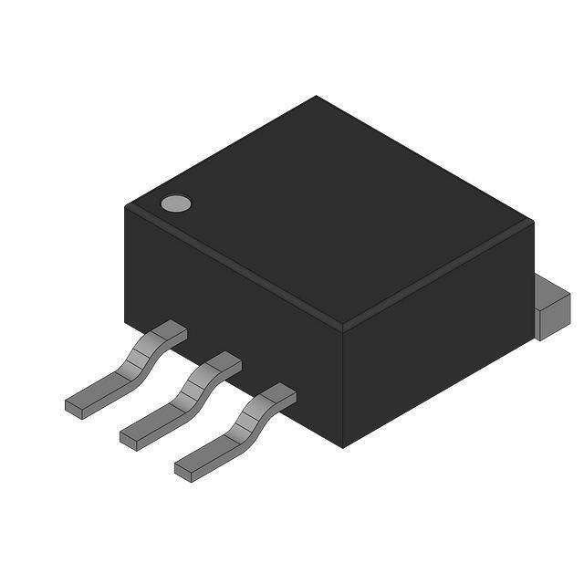
D²PAK
Features
•�Ideal�for�hot-swap�and�e-fuse�applications
•�Very�low�on-resistance��RDS(on)
•�Wide�safe�operating�area�SOA
•�N-channel,�normal�level
•�100%�avalanche�tested
•�Pb-free�plating;�RoHS�compliant
•�Qualified�according�to�JEDEC1)��for�target�applications
•�Halogen-free�according�to�IEC61249-2-21
Table�1�����Key�Performance�Parameters
Parameter
Value
Unit
VDS
100
V
RDS(on),max
3.3
mΩ
ID�(silicon�limited)
170
A
ID�(package�limited)
120
A
Ipulse�(VDS=56�V,�tp=10
7
ms)
Gate
Pin 1
Source
Pin 3
A
Type�/�Ordering�Code
Package
IPB033N10N5LF
PG-TO 263-3
1)
Drain
Pin 2, Tab
Marking
033N10LF
Related�Links
-
J-STD20 and JESD22
Final Data Sheet
1
Rev.�2.1,��2017-02-16
�OptiMOSTM�5�Linear�FET,�100�V
IPB033N10N5LF
Table�of�Contents
Description . . . . . . . . . . . . . . . . . . . . . . . . . . . . . . . . . . . . . . . . . . . . . . . . . . . . . . . . . . . . . . . . . . . . . . . . . . . . . 1
Maximum ratings . . . . . . . . . . . . . . . . . . . . . . . . . . . . . . . . . . . . . . . . . . . . . . . . . . . . . . . . . . . . . . . . . . . . . . . . 3
Thermal characteristics . . . . . . . . . . . . . . . . . . . . . . . . . . . . . . . . . . . . . . . . . . . . . . . . . . . . . . . . . . . . . . . . . . . . 3
Electrical characteristics . . . . . . . . . . . . . . . . . . . . . . . . . . . . . . . . . . . . . . . . . . . . . . . . . . . . . . . . . . . . . . . . . . . 4
Electrical characteristics diagrams . . . . . . . . . . . . . . . . . . . . . . . . . . . . . . . . . . . . . . . . . . . . . . . . . . . . . . . . . . . 6
Package Outlines . . . . . . . . . . . . . . . . . . . . . . . . . . . . . . . . . . . . . . . . . . . . . . . . . . . . . . . . . . . . . . . . . . . . . . . 10
Revision History . . . . . . . . . . . . . . . . . . . . . . . . . . . . . . . . . . . . . . . . . . . . . . . . . . . . . . . . . . . . . . . . . . . . . . . . 11
Trademarks . . . . . . . . . . . . . . . . . . . . . . . . . . . . . . . . . . . . . . . . . . . . . . . . . . . . . . . . . . . . . . . . . . . . . . . . . . . 11
Disclaimer . . . . . . . . . . . . . . . . . . . . . . . . . . . . . . . . . . . . . . . . . . . . . . . . . . . . . . . . . . . . . . . . . . . . . . . . . . . . 11
Final Data Sheet
2
Rev.�2.1,��2017-02-16
�OptiMOSTM�5�Linear�FET,�100�V
IPB033N10N5LF
1�����Maximum�ratings
at�TA=25�°C,�unless�otherwise�specified
Table�2�����Maximum�ratings
Parameter
Symbol
Continuous drain current
Values
Unit
Note�/�Test�Condition
120
108
23
A
VGS=10�V,�TC=25�°C
VGS=10�V,�TC=100�°C
VGS=10�V,�TC=25�°C,�RthJA�=40�K/W1)
-
480
A
TC=25�°C
-
-
273
mJ
ID=100�A,�RGS=25�Ω
VGS
-20
-
20
V
-
Power dissipation
Ptot
-
-
179
W
TC=25�°C
Operating and storage temperature
Tj,�Tstg
-55
-
150
°C
IEC climatic category;
DIN IEC 68-1: 55/150/56
Unit
Note�/�Test�Condition
Min.
Typ.
Max.
ID
-
-
Pulsed drain current2)
ID,pulse
-
Avalanche energy, single pulse3)
EAS
Gate source voltage
2�����Thermal�characteristics
Table�3�����Thermal�characteristics
Parameter
Symbol
Thermal resistance, junction - case
Values
Min.
Typ.
Max.
RthJC
-
0.45
0.7
K/W
-
Device on PCB,
minimal footprint
RthJA
-
-
62
K/W
-
Device on PCB,
6 cm² cooling area1)
RthJA
-
-
40
K/W
-
1)
Device on 40 mm x 40 mm x 1.5 mm epoxy PCB FR4 with 6 cm2 (one layer, 70 µm thick) copper area for drain
connection. PCB is vertical in still air.
2)
See Diagram 3 for more detailed information
3)
See Diagram 13 for more detailed information
Final Data Sheet
3
Rev.�2.1,��2017-02-16
�OptiMOSTM�5�Linear�FET,�100�V
IPB033N10N5LF
3�����Electrical�characteristics
Table�4�����Static�characteristics
Parameter
Symbol
Drain-source breakdown voltage
Values
Unit
Note�/�Test�Condition
-
V
VGS=0�V,�ID=1�mA
3.3
4.1
V
VDS=VGS,�ID=150�µA
-
1
10
10
100
µA
VDS=100�V,�VGS=0�V,�Tj=25�°C
VDS=100�V,�VGS=0�V,�Tj=125�°C
IGSS
-
2
-2
5
-5
µA
VGS=20�V,�VDS=0�V
VGS=-10�V,�VDS=0�V
RDS(on)
-
2.7
3.3
mΩ
VGS=10�V,�ID=100�A
Gate resistance
RG
-
40
60
Ω
-
Transconductance
gfs
23
46
-
S
|VDS|>2|ID|RDS(on)max,�ID=100�A
Unit
Note�/�Test�Condition
Min.
Typ.
Max.
V(BR)DSS
100
-
Gate threshold voltage
VGS(th)
2.5
Zero gate voltage drain current
IDSS
Gate-source leakage current
Drain-source on-state resistance
1)
Table�5�����Dynamic�characteristics1)�
Parameter
Symbol
Input capacitance
Values
Min.
Typ.
Max.
Ciss
-
350
460
pF
VGS=0�V,�VDS=50�V,�f=1�MHz
Output capacitance
Coss
-
1100
1400
pF
VGS=0�V,�VDS=50�V,�f=1�MHz
Reverse transfer capacitance
Crss
-
13
-
pF
VGS=0�V,�VDS=50�V,�f=1�MHz
Turn-on delay time
td(on)
-
8
-
ns
VDD=50�V,�VGS=10�V,�ID=50�A,
RG,ext=1.6�Ω
Rise time
tr
-
32
-
ns
VDD=50�V,�VGS=10�V,�ID=50�A,
RG,ext=1.6�Ω
Turn-off delay time
td(off)
-
64
-
ns
VDD=50�V,�VGS=10�V,�ID=50�A,
RG,ext=1.6�Ω
Fall time
tf
-
48
-
ns
VDD=50�V,�VGS=10�V,�ID=50�A,
RG,ext=1.6�Ω
Unit
Note�/�Test�Condition
Table�6�����Gate�charge�characteristics2)�
Parameter
Symbol
Values
Min.
Typ.
Max.
Qgs
-
3
-
nC
VDD=50�V,�ID=100�A,�VGS=0�to�10�V
Qgd
-
72
-
nC
VDD=50�V,�ID=100�A,�VGS=0�to�10�V
Gate charge total
Qg
-
102
-
nC
VDD=50�V,�ID=100�A,�VGS=0�to�10�V
Gate plateau voltage
Vplateau
-
6.9
-
V
VDD=50�V,�ID=100�A,�VGS=0�to�10�V
Qoss
-
116
-
nC
VDD=50�V,�VGS=0�V
Gate to source charge
1)
Gate to drain charge
1)
1)
Output charge
1)
2)
Defined by design. Not subject to production test.
See ″Gate charge waveforms″ for parameter definition
Final Data Sheet
4
Rev.�2.1,��2017-02-16
�OptiMOSTM�5�Linear�FET,�100�V
IPB033N10N5LF
Table�7�����Reverse�diode
Parameter
Symbol
Diode continuous forward current
Diode pulse current
Diode forward voltage
1)
Reverse recovery time
1)
Reverse recovery charge
1)
Values
Unit
Note�/�Test�Condition
120
A
TC=25�°C
-
480
A
TC=25�°C
-
0.93
1.2
V
VGS=0�V,�IF=100�A,�Tj=25�°C
trr
-
58
-
ns
VR=50�V,�IF=50A,�diF/dt=100�A/µs
Qrr
-
94
-
nC
VR=50�V,�IF=50A,�diF/dt=100�A/µs
Min.
Typ.
Max.
IS
-
-
IS,pulse
-
VSD
Defined by design. Not subject to production test.
Final Data Sheet
5
Rev.�2.1,��2017-02-16
�OptiMOSTM�5�Linear�FET,�100�V
IPB033N10N5LF
4�����Electrical�characteristics�diagrams
Diagram�1:�Power�dissipation
Diagram�2:�Drain�current
200
200
limited by package
limited by silicon
160
150
ID�[A]
Ptot�[W]
120
100
80
50
40
0
0
25
50
75
100
125
150
0
175
0
25
50
TC�[°C]
75
100
125
150
175
TC�[°C]
Ptot=f(TC)
ID=f(TC);�VGS≥10�V
Diagram�3:�Safe�operating�area
Diagram�4:�Max.�transient�thermal�impedance
3
100
10
1 µs
0.5
10 µs
0.2
10 ms
2
10
10
1 ms
ID�[A]
0.1
ZthJC�[K/W]
100 µs
-1
DC
101
0.05
0.02
0.01
10-2
single pulse
100
10-1
100
101
102
103
10-3
10-6
10-5
10-4
VDS�[V]
10-2
10-1
100
tp�[s]
ID=f(VDS);�TC=25�°C;�D=0;�parameter:�tp
Final Data Sheet
10-3
ZthJC=f(tp);�parameter:�D=tp/T
6
Rev.�2.1,��2017-02-16
�OptiMOSTM�5�Linear�FET,�100�V
IPB033N10N5LF
Diagram�5:�Typ.�output�characteristics
Diagram�6:�Typ.�drain-source�on�resistance
70
4.0
3.5
60
10 V
3.0
50
8V
2.5
RDS(on)��[mΩ]
ID�[A]
40
8V
30
6V
20
10
10 V
2.0
1.5
5.5 V
1.0
5V
0.5
4.5 V
0
0
1
2
3
4
0.0
5
0
20
40
VDS�[V]
60
80
ID=f(VDS);�Tj=25�°C,�tp=30�µs;�parameter:�VGS
RDS(on)=f(ID);�Tj=25�°C;�parameter:�VGS
Diagram�7:�Typ.�transfer�characteristics
Diagram�8:�Typ.�forward�transconductance
60
60
50
50
40
40
gfs�[S]
ID�[A]
100
ID�[A]
30
20
30
20
10
10
150 °C
25 °C
0
0
1
2
3
4
5
6
7
0
0
20
VGS�[V]
60
80
100
120
ID�[A]
ID=f(VGS);�VDS=10�V;�parameter:�Tj
Final Data Sheet
40
gfs=f(ID);�Tj=25�°C
7
Rev.�2.1,��2017-02-16
�OptiMOSTM�5�Linear�FET,�100�V
IPB033N10N5LF
Diagram�9:�Normalized�drain-source�on-state�resistance
Diagram�10:�Typ.�gate�threshold�voltage
2.00
4
1.75
1500 µA
3
150 µA
1.25
VGS(th)�[V]
RDS(on),�normalized�to�25�°C
1.50
1.00
2
0.75
0.50
1
0.25
0.00
-80
-40
0
40
80
120
0
-60
160
-20
20
60
Tj�[°C]
100
140
180
Tj�[°C]
RDS(on)=f(Tj),�ID=100�A,�VGS=10�V
VGS(th)=f(Tj);�VGS=VDS
Diagram�11:�Typ.�capacitances
Diagram�12:�Forward�characteristics�of�reverse�diode
4
103
10
25 °C
25 °C, max
150 °C
150 °C, max
Coss
IF�[A]
102
C�[pF]
103
Ciss
102
101
101
Crss
0
20
40
60
80
100
100
0.0
0.5
VDS�[V]
1.5
2.0
2.5
VSD�[V]
C=f(VDS);�VGS=0�V;�f=1�MHz
Final Data Sheet
1.0
IF=f(VSD);�parameter:�Tj
8
Rev.�2.1,��2017-02-16
�OptiMOSTM�5�Linear�FET,�100�V
IPB033N10N5LF
Diagram�13:�Avalanche�characteristics
Diagram�14:�Typ.�gate�charge
3
10
12
10
20 V
102
50 V
8
80 V
VGS�[V]
IAV�[A]
25 °C
100 °C
101
6
4
125 °C
2
100
100
101
102
103
0
0
25
tAV�[µs]
50
75
100
125
Qgate�[nC]
IAS=f(tAV);�RGS=25�Ω;�parameter:�Tj(start)
VGS=f(Qgate);�ID=100�A�pulsed,�resistive�load;�parameter:�VDD
Diagram�15:�Drain-source�breakdown�voltage
Gate charge waveforms
110
VBR(DSS)�[V]
105
100
95
-60
-20
20
60
100
140
180
Tj�[°C]
VBR(DSS)=f(Tj);�ID=1�mA
Final Data Sheet
9
Rev.�2.1,��2017-02-16
�OptiMOSTM�5�Linear�FET,�100�V
IPB033N10N5LF
5�����Package�Outlines
Figure�1�����Outline�PG-TO�263-3,�dimensions�in�mm/inches
Final Data Sheet
10
Rev.�2.1,��2017-02-16
�OptiMOSTM�5�Linear�FET,�100�V
IPB033N10N5LF
Revision�History
IPB033N10N5LF
Revision:�2017-02-16,�Rev.�2.1
Previous Revision
Revision
Date
Subjects (major changes since last revision)
2.0
2016-12-15
Release of final version
2.1
2017-02-16
Update technology heading
Trademarks�of�Infineon�Technologies�AG
AURIX™,�C166™,�CanPAK™,�CIPOS™,�CoolGaN™,�CoolMOS™,�CoolSET™,�CoolSiC™,�CORECONTROL™,�CROSSAVE™,�DAVE™,�DI-POL™,�DrBlade™,
EasyPIM™,�EconoBRIDGE™,�EconoDUAL™,�EconoPACK™,�EconoPIM™,�EiceDRIVER™,�eupec™,�FCOS™,�HITFET™,�HybridPACK™,�Infineon™,
ISOFACE™,�IsoPACK™,�i-Wafer™,�MIPAQ™,�ModSTACK™,�my-d™,�NovalithIC™,�OmniTune™,�OPTIGA™,�OptiMOS™,�ORIGA™,�POWERCODE™,
PRIMARION™,�PrimePACK™,�PrimeSTACK™,�PROFET™,�PRO-SIL™,�RASIC™,�REAL3™,�ReverSave™,�SatRIC™,�SIEGET™,�SIPMOS™,�SmartLEWIS™,
SOLID�FLASH™,�SPOC™,�TEMPFET™,�thinQ�™,�TRENCHSTOP™,�TriCore™.
Trademarks�updated�August�2015
Other�Trademarks
All�referenced�product�or�service�names�and�trademarks�are�the�property�of�their�respective�owners.
We�Listen�to�Your�Comments
Any�information�within�this�document�that�you�feel�is�wrong,�unclear�or�missing�at�all?�Your�feedback�will�help�us�to�continuously
improve�the�quality�of�this�document.�Please�send�your�proposal�(including�a�reference�to�this�document)�to:
erratum@infineon.com
Published�by
Infineon�Technologies�AG
81726�München,�Germany
©�2017�Infineon�Technologies�AG
All�Rights�Reserved.
Legal�Disclaimer
The�information�given�in�this�document�shall�in�no�event�be�regarded�as�a�guarantee�of�conditions�or�characteristics�
(“Beschaffenheitsgarantie”)�.
With�respect�to�any�examples,�hints�or�any�typical�values�stated�herein�and/or�any�information�regarding�the�application�of�the
product,�Infineon�Technologies�hereby�disclaims�any�and�all�warranties�and�liabilities�of�any�kind,�including�without�limitation
warranties�of�non-infringement�of�intellectual�property�rights�of�any�third�party.
In�addition,�any�information�given�in�this�document�is�subject�to�customer’s�compliance�with�its�obligations�stated�in�this
document�and�any�applicable�legal�requirements,�norms�and�standards�concerning�customer’s�products�and�any�use�of�the
product�of�Infineon�Technologies�in�customer’s�applications.
The�data�contained�in�this�document�is�exclusively�intended�for�technically�trained�staff.�It�is�the�responsibility�of�customer’s
technical�departments�to�evaluate�the�suitability�of�the�product�for�the�intended�application�and�the�completeness�of�the�product
information�given�in�this�document�with�respect�to�such�application.
Information
For�further�information�on�technology,�delivery�terms�and�conditions�and�prices�please�contact�your�nearest�Infineon
Technologies�Office�(www.infineon.com).
Warnings
Due�to�technical�requirements,�components�may�contain�dangerous�substances.�For�information�on�the�types�in�question,
please�contact�the�nearest�Infineon�Technologies�Office.
The�Infineon�Technologies�component�described�in�this�Data�Sheet�may�be�used�in�life-support�devices�or�systems�and/or
automotive,�aviation�and�aerospace�applications�or�systems�only�with�the�express�written�approval�of�Infineon�Technologies,�if�a
failure�of�such�components�can�reasonably�be�expected�to�cause�the�failure�of�that�life-support,�automotive,�aviation�and
aerospace�device�or�system�or�to�affect�the�safety�or�effectiveness�of�that�device�or�system.�Life�support�devices�or�systems�are
intended�to�be�implanted�in�the�human�body�or�to�support�and/or�maintain�and�sustain�and/or�protect�human�life.�If�they�fail,�it�is
reasonable�to�assume�that�the�health�of�the�user�or�other�persons�may�be�endangered.
Final Data Sheet
11
Rev.�2.1,��2017-02-16
�