IPB90R340C3
CoolMOS™ Power Transistor
Product Summary
Features
• Lowest figure-of-merit RON x Qg
• Extreme dv/dt rated
VDS @ TJ=25°C
900
V
RDS(on),max @TJ=25°C
0.34
W
94
nC
Qg,typ
• High peak current capability
• Qualified according to JEDEC1) for industrial applications
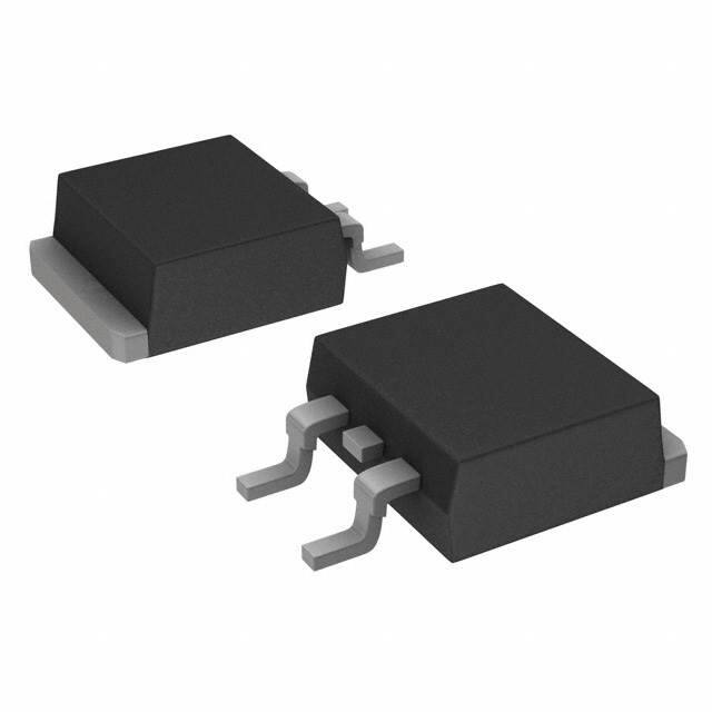
PG-TO263
• Pb-free lead plating; RoHS compliant
• Ultra low gate charge
CoolMOS™ 900V is designed for:
• Quasi Resonant Flyback / Forward topologies
• SMPS
• PC Silverbox
• Lighting
• Solar
Type
Package
Marking
IPB90R340C3
PG-TO263
9R340C
Maximum ratings, at T J=25 °C, unless otherwise specified
Parameter
Symbol Conditions
Continuous drain current
ID
Value
T C=25 °C
15
T C=100 °C
9.5
Pulsed drain current 2)
I D,pulse
T C=25 °C
34
Avalanche energy, single pulse
E AS
I D=3.1 A, V DD=50 V
678
Avalanche energy, repetitive t AR 2),3)
E AR
I D=3.1 A, V DD=50 V
1
Avalanche current, repetitive t AR 2),3)
I AR
MOSFET dv /dt ruggedness
dv /dt
Gate source voltage
V GS
Power dissipation
P tot
Operating and storage temperature
T J, T stg
Rev. 2.0
Unit
A
mJ
3.1
A
V DS=0...400 V
50
V/ns
static
±20
V
AC (f>1 Hz)
±30
T C=25 °C
208
W
-55 ... 150
°C
page 1
2012-04-16
�IPB90R340C3
Maximum ratings, at T J=25 °C, unless otherwise specified
Parameter
Symbol
Continuous diode forward current
IS
Diode pulse current 2)
Reverse diode dv /dt
4)
Parameter
Value
Conditions
Unit
9.2
A
T C=25 °C
I S,pulse
34
dv /dt
4
V/ns
Values
Unit
Symbol
Conditions
min.
typ.
max.
-
-
0.6
-
-
62
-
35
-
-
-
260
°C
V
Thermal characteristics
Thermal resistance, junction - case
R thJC
R thJA
Thermal resistance, junction ambient
R thJA
SMD version, device
on PCB: at minimum
footprint
SMD version, device
on PCB: at 6 cm²
cooling area
Soldering temperature, only reflow
soldering allowed; part not qualified
for direct wave soldering but bottom
side PCB wave soldering is allowed
T sold
K/W
5)
reflow MSL1
Electrical characteristics, at T J=25 °C, unless otherwise specified
Static characteristics
Drain-source breakdown voltage
V (BR)DSS V GS=0 V, I D=250 µA
900
-
-
Gate threshold voltage
V GS(th)
V DS=V GS, I D=1 mA
2.5
3
3.5
Zero gate voltage drain current
I DSS
V DS=900 V, V GS=0 V,
T j=25 °C
-
-
2
V DS=900 V, V GS=0 V,
T j=150 °C
-
20
-
µA
Gate-source leakage current
I GSS
V GS=20 V, V DS=0 V
-
-
100
nA
Drain-source on-state resistance
R DS(on)
V GS=10 V, I D=9.2 A,
T j=25 °C
-
0.28
0.34
W
V GS=10 V, I D=9.2 A,
T j=150 °C
-
0.76
-
f =1 MHz, open drain
-
1.3
-
Gate resistance
Rev. 2.0
RG
page 2
W
2012-04-16
�IPB90R340C3
Parameter
Values
Symbol Conditions
Unit
min.
typ.
max.
-
2400
-
-
120
-
-
71
-
-
280
-
-
70
-
-
20
-
-
400
-
Dynamic characteristics
Input capacitance
C iss
Output capacitance
C oss
Effective output capacitance, energy
C o(er)
related 6)
V GS=0 V, V DS=100 V,
f =1 MHz
V GS=0 V, V DS=0 V
to 500 V
pF
Effective output capacitance, time
related 7)
C o(tr)
Turn-on delay time
t d(on)
Rise time
tr
Turn-off delay time
t d(off)
Fall time
tf
-
25
-
Gate to source charge
Q gs
-
11
-
Gate to drain charge
Q gd
-
41
-
Gate charge total
Qg
-
94
-
Gate plateau voltage
V plateau
-
4.6
-
V
-
0.8
1.2
V
-
510
-
ns
-
11
-
µC
-
41
-
A
V DD=400 V,
V GS=10 V, I D=9.2A,
R G=23.1 W
ns
Gate Charge Characteristics
V DD=400 V, I D=9.2 A,
V GS=0 to 10 V
nC
Reverse Diode
Diode forward voltage
V SD
Reverse recovery time
t rr
Reverse recovery charge
Q rr
Peak reverse recovery current
I rrm
V GS=0 V, I F=9.2 A,
T j=25 °C
V R=400 V, I F=I S,
di F/dt =100 A/µs
1)
J-STD20 and JESD22
2)
Pulse width t p limited by T J,max
3)
Repetitive avalanche causes additional power losses that can be calculated as P AV=E AR*f.
4)
ISD≤ID, di/dt≤200A/µs, VDClink=400V, Vpeak