IPBE65R230CFD7AATMA1

IPBE65R230CFD7AATMA1

  • 厂商:

    EUPEC(英飞凌)

  • 封装:

    TO-263-7(D2PAK)

  • 描述:

  • 详情介绍
  • 数据手册
  • 价格&库存
IPBE65R230CFD7AATMA1 数据手册
IPBE65R230CFD7A MOSFET 650VCoolMOSªCFD7ASJPowerDevice D²-PAK7pin 650VCoolMOS™CFD7AisInfineon'slatestgenerationofmarketleading automotivequalifiedhighvoltageCoolMOS™MOSFETs.Inadditiontothe well-knownattributesofhighqualityandreliabilityrequiredbythe automotiveindustry,thenewCoolMOS™CFD7Aseriesprovidesforan integratedfastbodydiodeandcanbeusedforPFCandresonant switchingtopologiesliketheZVSphase-shiftfull-bridgeandLLC. tab 1 Features 2 3 45 6 7 •Latest650Vautomotivequalifiedtechnologywithintegratedfastbody diodeonthemarketfeaturingultralowQrr •LowestFOMRDS(on)*QgandRDS(on)*Eoss •100%avalanchetested •Kelvinsourcecontactavailable •Best-in-classRDS(on)inSMDandTHDpackages Drain tab Gate Pin 1 Benefits *1 *2 •Optimizedforhigherbatteryvoltagesupto475Vthankstofurther improvedrobustness •Lowerswitchinglossesenablinghigherswitchingfrequencies •Highqualityandreliability •Advancedcontrollabilityduetokelvinsource •Increasedpackagecreepagedistance •Increasedefficiencyinlightloadandfullloadconditions *1: Internal body diode *2: Integrated ESD diode Power Source Pin 3-7 Driver Source Pin 2 Potentialapplications SuitableforPFCandDC-DCstagesfor: •UnidirectionalandbidirectionalDC-DCconverters, •On-BoardbatteryChargers Productvalidation QualifiedaccordingtoAECQ101 Pleasenote:Thesourceandsensesourcepinsarenotexchangeable. Theirexchangemightleadtomalfunction.Forproductionpartapproval process(PPAP)releaseweproposetoshareapplicationrelated informationduringanearlydesignphasetoavoiddelaysinPPAPrelease. PleasecontactInfineonsalesoffice. Table1KeyPerformanceParameters Parameter Value Unit VDS 650 V RDS(on),max 230 mΩ Qg,typ 23 nC ID,pulse 44 A Eoss @ 400V 3.0 µJ Body diode diF/dt 1300 A/µs Type/OrderingCode Package IPBE65R230CFD7A PG-TO263-7-11 Final Data Sheet 1 Marking RelatedLinks 65A230F7 see Appendix A Rev.2.2,2021-11-24 650VCoolMOSªCFD7ASJPowerDevice IPBE65R230CFD7A TableofContents Description . . . . . . . . . . . . . . . . . . . . . . . . . . . . . . . . . . . . . . . . . . . . . . . . . . . . . . . . . . . . . . . . . . . . . . . . . . . . . 1 Maximum ratings . . . . . . . . . . . . . . . . . . . . . . . . . . . . . . . . . . . . . . . . . . . . . . . . . . . . . . . . . . . . . . . . . . . . . . . . 3 Thermal characteristics . . . . . . . . . . . . . . . . . . . . . . . . . . . . . . . . . . . . . . . . . . . . . . . . . . . . . . . . . . . . . . . . . . . . 4 Electrical characteristics . . . . . . . . . . . . . . . . . . . . . . . . . . . . . . . . . . . . . . . . . . . . . . . . . . . . . . . . . . . . . . . . . . . 5 Electrical characteristics diagrams . . . . . . . . . . . . . . . . . . . . . . . . . . . . . . . . . . . . . . . . . . . . . . . . . . . . . . . . . . . 7 Test Circuits . . . . . . . . . . . . . . . . . . . . . . . . . . . . . . . . . . . . . . . . . . . . . . . . . . . . . . . . . . . . . . . . . . . . . . . . . . . 11 Package Outlines . . . . . . . . . . . . . . . . . . . . . . . . . . . . . . . . . . . . . . . . . . . . . . . . . . . . . . . . . . . . . . . . . . . . . . . 12 Appendix A . . . . . . . . . . . . . . . . . . . . . . . . . . . . . . . . . . . . . . . . . . . . . . . . . . . . . . . . . . . . . . . . . . . . . . . . . . . . 13 Revision History . . . . . . . . . . . . . . . . . . . . . . . . . . . . . . . . . . . . . . . . . . . . . . . . . . . . . . . . . . . . . . . . . . . . . . . . 14 Trademarks . . . . . . . . . . . . . . . . . . . . . . . . . . . . . . . . . . . . . . . . . . . . . . . . . . . . . . . . . . . . . . . . . . . . . . . . . . . 14 Disclaimer . . . . . . . . . . . . . . . . . . . . . . . . . . . . . . . . . . . . . . . . . . . . . . . . . . . . . . . . . . . . . . . . . . . . . . . . . . . . 14 Final Data Sheet 2 Rev.2.2,2021-11-24 650VCoolMOSªCFD7ASJPowerDevice IPBE65R230CFD7A 1Maximumratings atTj=25°C,unlessotherwisespecified Table2Maximumratings Parameter Symbol Continuous drain current1) Values Unit Note/TestCondition 11 7 A TC=25°C TC=100°C - 44 A TC=25°C - - 52 mJ ID=3.0A; VDD=50V; see table 10 IAS - - 3.0 A - MOSFET dv/dt ruggedness dv/dt - - 120 V/ns VDS=0...400V Gate source voltage (static) VGS -20 - 20 V static; Gate source voltage (dynamic) VGSk,pulse -30 - 30 V frepetition
IPBE65R230CFD7AATMA1
物料型号:IPBE65R230CFD7A

器件简介: - 650V CoolMOS™ CFD7A是英飞凌最新一代的汽车级高电压CoolMOS™ MOSFET。 - 集成了快速体二极管,适用于PFC和ZVS移相全桥、LLC等谐振开关拓扑。
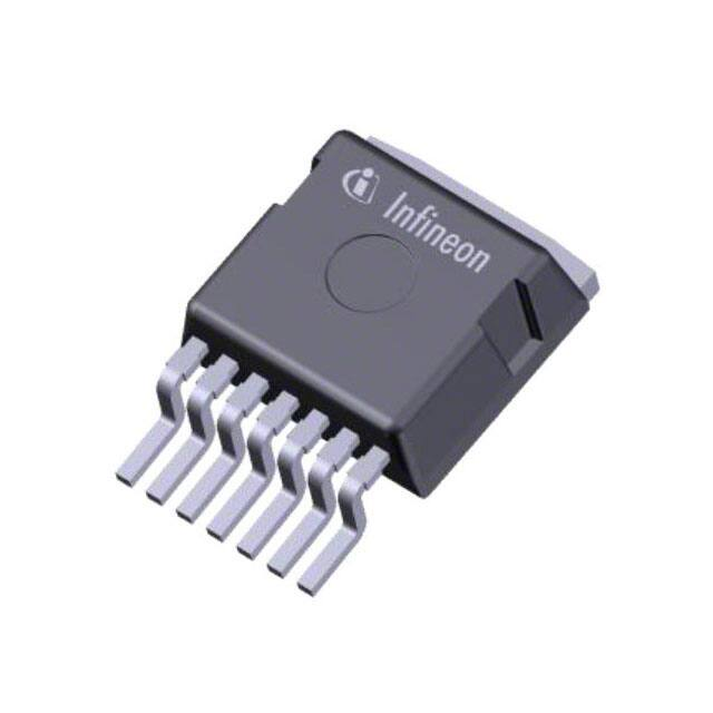
引脚分配: - 采用D-PAK 7pin封装,包括Kelvin源接触,引脚2为源极,引脚3-7为漏极。

参数特性: - 100%雪崩测试,优化用于高达475V的更高电池电压。 - 降低开关损耗,提高开关频率,提高轻载和满载条件下的效率。

功能详解: - 适用于PFC和DC-DC阶段,包括单向和双向DC-DC转换器、车载电池充电器。

应用信息: - 根据AEC Q101标准进行认证,注意源极和感应源极引脚不可交换。

封装信息: - 封装类型为PG-TO263-7-11,标记为65A230F7。

关键性能参数: - 漏源电压(VDs):650V - 导通电阻(Ros(on).max):230mΩ - 栅极电荷(Qg.typ):23nC - 脉冲漏极电流(Io.pulse):44A - 漏极-源极偏置电压下的输出电荷(Eoss @ 400V):3.0FJ - 体二极管di/dt:1300A/s

最大额定值: - 连续漏极电流:10A至117A - 脉冲漏极电流:44A - 雪崩能量:52mJ - MOSFET dv/dt耐量:120V/ns

热特性: - 结-壳热阻:1.99°C/W - 允许的焊接温度:260°C

电气特性: - 漏源击穿电压:650V - 栅极阈值电压:3.5V至4.5V - 栅极-源极漏电流:最大1A - 导通电阻:最小0.196mΩ,典型值0.230mΩ

动态特性: - 输入电容:典型值1044pF - 输出电容:典型值17pF - 导通延迟时间:典型值13ns - 上升时间:典型值3ns

门极电荷特性: - 门极-源极电荷:典型值6nC - 门极-漏极电荷:典型值7nC - 总门极电荷:典型值23nC

反向二极管特性: - 二极管正向电压:典型值1.1V - 反向恢复时间:典型值91ns - 反向恢复电荷:典型值0.4uC

测试电路和封装轮廓也包含在文档中,提供了详细的测试条件和布局建议。

修订历史: - 最终数据手册的修订日期为2021年11月24日,版本号为Rev.2.2。

免责声明: - 文档中的信息不构成对条件或特性的保证,且不承担任何明示或暗示的保证,包括对第三方知识产权的非侵权保证。
IPBE65R230CFD7AATMA1 价格&库存

很抱歉,暂时无法提供与“IPBE65R230CFD7AATMA1”相匹配的价格&库存,您可以联系我们找货

免费人工找货
IPBE65R230CFD7AATMA1

    库存:0

    IPBE65R230CFD7AATMA1
    •  国内价格
    • 1+27.98640
    • 200+23.32200
    • 500+18.65760
    • 1000+15.54800

    库存:0

    IPBE65R230CFD7AATMA1
    •  国内价格 香港价格
    • 1+37.362141+4.79210
    • 10+24.4965910+3.14195
    • 100+17.18430100+2.20407
    • 500+14.30720500+1.83506

    库存:975

    IPBE65R230CFD7AATMA1
    •  国内价格 香港价格
    • 1000+13.061221000+1.67524
    • 2000+12.218942000+1.56721
    • 3000+11.789903000+1.51219
    • 5000+11.688825000+1.49922

    库存:975