MOSFET
Metal�Oxide�Semiconductor�Field�Effect�Transistor
OptiMOS™�Power-Transistor,�120V
OptiMOS™�3�Power-Transistor
IPD_S110N12N3�G
Data�Sheet
Rev.�2.4
Final
Industrial�&�Multimarket
�IPD110N12N3 G
IPS110N12N3 G
OptiMOSTM3Power-Transistor
Product Summary
Features
• N-channel, normal level
• Excellent gate charge x R DS(on) product (FOM)
VDS
120
V
RDS(on),max
11
mΩ
ID
75
A
• Very low on-resistance R DS(on)
• 175 °C operating temperature
• Pb-free lead plating; RoHS compliant
• Qualified according to JEDEC1) for target application
• Halogen free according to IEC61249-2-21 *
• Ideal for high-frequency switching and synchronous rectification
Type
IPS110N12N3 G
IPD110N12N3 G
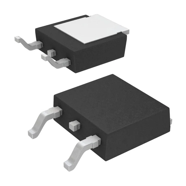
Package
PG-TO251-3
PG-TO252-3
Marking
110N12N
110N12N
Maximum ratings, at T j=25 °C, unless otherwise specified
Parameter
Symbol Conditions
Continuous drain current
ID
Value
T C=25 °C
75
T C=100 °C
54
Unit
A
Pulsed drain current2)
I D,pulse
T C=25 °C
300
Avalanche energy, single pulse
E AS
I D=75 A, R GS=25 Ω
120
mJ
Gate source voltage3)
V GS
±20
V
136
W
-55 ... 175
°C
P tot
Operating and storage temperature
T C=25 °C
T j, T stg
IEC climatic category; DIN IEC 68-1
1)
55/175/56
J-STD20 and JESD22
2)
see figure 3
3)
Tjmax=150°C and duty cycle D=0.01 for Vgs2|I D|R DS(on)max,
I D=75 A
4)
Device on 40 mm x 40 mm x 1.5 mm epoxy PCB FR4 with 6 cm 2 (one layer, 70 µm thick) copper area for drain
connection. PCB is vertical in still air.
Rev. 2.4
page 2
2015-06-24
�IPD110N12N3 G
IPS110N12N3 G
Parameter
Values
Symbol Conditions
Unit
min.
typ.
max.
-
3240
4310
-
408
543
Dynamic characteristics6)
Input capacitance
C iss
Output capacitance
C oss
Reverse transfer capacitance
C rss
-
22
-
Turn-on delay time
t d(on)
-
16
-
Rise time
tr
-
16
-
Turn-off delay time
t d(off)
-
24
-
Fall time
tf
-
8
-
Gate to source charge
Q gs
-
18
-
Gate to drain charge
Q gd
-
12
-
-
20
-
V GS=0 V, V DS=60 V,
f =1 MHz
V DD=60 V, V GS=10 V,
I D=75 A, R G,ext=1.6 Ω
pF
ns
Gate Charge Characteristics5)
V DD=60 V, I D=75 A,
V GS=0 to 10 V
nC
Switching charge
Q sw
Gate charge total6)
Qg
-
49
65
Gate plateau voltage
V plateau
-
5.6
-
Output charge6)
Q oss
-
56
75
nC
-
-
75
A
-
-
300
-
1
1.2
-
90
ns
-
249
nC
V DD=60 V, V GS=0 V
V
Reverse Diode
Diode continous forward current
IS
Diode pulse current
I S,pulse
Diode forward voltage
V SD
t rr
Reverse recovery charge
Q rr
5)
See figure 16 for gate charge parameter definition
6)
Defined by design. Not subject to production test
Rev. 2.4
T C=25 °C
V GS=0 V, I F=75 A,
T j=25 °C
V R=60 V, I F=I S,
di F/dt =100 A/µs
page 3
V
2015-06-24
�IPD110N12N3 G
IPS110N12N3 G
1 Power dissipation
2 Drain current
P tot=f(T C)
I D=f(T C); V GS≥10 V
140
80
70
120
60
100
ID [A]
Ptot [W]
50
80
40
60
30
40
20
20
10
0
0
0
50
100
150
200
0
50
TC [°C]
100
150
200
TC [°C]
3 Safe operating area
4 Max. transient thermal impedance
I D=f(V DS); T C=25 °C; D =0
Z thJC=f(t p)
parameter: t p
parameter: D =t p/T
103
101
1 µs
10 µs
102
100 µs
100
DC
101
0.5
ZthJC [K/W]
ID [A]
1 ms
10 ms
0.2
0.1
10-1
0.05
0.02
100
0.01
single pulse
10-1
10-2
10-1
100
101
102
103
VDS [V]
Rev. 2.4
10-5
10-4
10-3
10-2
10-1
100
tp [s]
page 4
2015-06-24
�IPD110N12N3 G
IPS110N12N3 G
5 Typ. output characteristics
6 Typ. drain-source on resistance
I D=f(V DS); T j=25 °C
R DS(on)=f(I D); T j=25 °C
parameter: V GS
parameter: V GS
250
30
10 V
8V
4.5 V
7V
5V
25
200
20
RDS(on) [mΩ]
5.5 V
150
ID [A]
6.5 V
100
6V
15
6V
10
10 V
5.5 V
50
5
5V
4.5 V
0
0
0
1
2
3
4
5
0
20
VDS [V]
40
60
80
60
80
ID [A]
7 Typ. transfer characteristics
8 Typ. forward transconductance
I D=f(V GS); |V DS|>2|I D|R DS(on)max
g fs=f(I D); T j=25 °C
parameter: T j
200
100
80
150
gfs [S]
ID [A]
60
100
40
175 °C
50
25 °C
20
0
0
0
2
4
6
8
VGS [V]
Rev. 2.4
0
20
40
ID [A]
page 5
2015-06-24
�IPD110N12N3 G
IPS110N12N3 G
9 Drain-source on-state resistance
10 Typ. gate threshold voltage
R DS(on)=f(T j); I D=75 A; V GS=10 V
V GS(th)=f(T j); V GS=V DS
parameter: I D
25
4
3.5
20
830 µA
3
VGS(th) [V]
RDS(on) [mΩ]
83 µA
2.5
15
98 %
typ
10
2
1.5
1
5
0.5
0
0
-60
-20
20
60
100
140
180
-60
-20
20
Tj [°C]
60
100
140
180
Tj [°C]
11 Typ. capacitances
12 Forward characteristics of reverse diode
C =f(V DS); V GS=0 V; f =1 MHz
I F=f(V SD)
parameter: T j
104
103
Ciss
25 °C
175 °C
103
175 °C, 98%
102
IF [A]
C [pF]
Coss
102
25 °C, 98%
101
Crss
101
100
0
20
40
60
80
100
VDS [V]
Rev. 2.4
0
0.5
1
1.5
2
VSD [V]
page 6
2015-06-24
�IPD110N12N3 G
IPS110N12N3 G
13 Avalanche characteristics
14 Typ. gate charge
I AS=f(t AV); R GS=25 Ω
V GS=f(Q gate); I D=67 A pulsed
parameter: T j(start)
parameter: V DD
103
10
96 V
8
60 V
102
24 V
VGS [V]
IAS [A]
6
25 °C
4
100 °C
150 °C
101
2
100
0
100
101
102
0
103
10
tAV [µs]
20
30
40
50
Qgate [nC]
15 Drain-source breakdown voltage
16 Gate charge waveforms
V BR(DSS)=f(T j); I D=1 mA
135
V GS
Qg
130
VBR(DSS) [V]
125
120
V g s(th)
115
110
Q g (th)
Q sw
Q gs
105
-60
-20
20
60
100
140
Q gate
Q gd
180
Tj [°C]
Rev. 2.4
page 7
2015-06-24
�IPD110N12N3 G
IPS110N12N3 G
PG-TO-251SL : Outline
Rev. 2.4
page 8
2015-06-24
�IPD110N12N3 G
IPS110N12N3 G
PG-TO252-3: Outline
Rev. 2.4
page 9
2015-06-24
�OptiMOS™�3�Power-Transistor
IPD_S110N12N3�G
Revision�History
IPD_S110N12N3 G
Revision:�2015-07-16,�Rev.�2.4
Previous Revision
Revision
Date
Subjects (major changes since last revision)
2.4
2015-07-16
Update VGS(th) and package outline TO252-3
We�Listen�to�Your�Comments
Any�information�within�this�document�that�you�feel�is�wrong,�unclear�or�missing�at�all?�Your�feedback�will�help�us�to�continuously
improve�the�quality�of�this�document.�Please�send�your�proposal�(including�a�reference�to�this�document)�to:
erratum@infineon.com
Published�by
Infineon�Technologies�AG
81726�München,�Germany
©�2015�Infineon�Technologies�AG
All�Rights�Reserved.
Legal�Disclaimer
The�information�given�in�this�document�shall�in�no�event�be�regarded�as�a�guarantee�of�conditions�or�characteristics.�With
respect�to�any�examples�or�hints�given�herein,�any�typical�values�stated�herein�and/or�any�information�regarding�the�application
of�the�device,�Infineon�Technologies�hereby�disclaims�any�and�all�warranties�and�liabilities�of�any�kind,�including�without
limitation,�warranties�of�non-infringement�of�intellectual�property�rights�of�any�third�party.
Information
For�further�information�on�technology,�delivery�terms�and�conditions�and�prices�please�contact�your�nearest�Infineon
Technologies�Office�(www.infineon.com).
Warnings
Due�to�technical�requirements,�components�may�contain�dangerous�substances.�For�information�on�the�types�in�question,
please�contact�the�nearest�Infineon�Technologies�Office.
The�Infineon�Technologies�component�described�in�this�Data�Sheet�may�be�used�in�life-support�devices�or�systems�and/or
automotive,�aviation�and�aerospace�applications�or�systems�only�with�the�express�written�approval�of�Infineon�Technologies,�if�a
failure�of�such�components�can�reasonably�be�expected�to�cause�the�failure�of�that�life-support,�automotive,�aviation�and
aerospace�device�or�system�or�to�affect�the�safety�or�effectiveness�of�that�device�or�system.�Life�support�devices�or�systems�are
intended�to�be�implanted�in�the�human�body�or�to�support�and/or�maintain�and�sustain�and/or�protect�human�life.�If�they�fail,�it�is
reasonable�to�assume�that�the�health�of�the�user�or�other�persons�may�be�endangered.
11
Rev.�2.4,��2015-07-16
�
很抱歉,暂时无法提供与“IPD110N12N3GBUMA1”相匹配的价格&库存,您可以联系我们找货
免费人工找货