IPD65R660CFDA
MOSFET
650V�CoolMOSª�CFDA�Power�Transistor
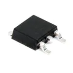
DPAK
CoolMOS™�is�a�revolutionary�technology�for�high�voltage�power
MOSFETs,�designed�according�to�the�superjunction�(SJ)�principle�and
pioneered�by�Infineon�Technologies.�650V�CoolMOS™�CFDA�series
combines�the�experience�of�the�leading�SJ�MOSFET�supplier�with�high
class�innovation.�The�resulting�devices�provide�all�benefits�of�a�fast
switching�SJ�MOSFET�while�offering�an�extremely�fast�and�robust�body
diode.�This�combination�of�extremely�low�switching,�commutation�and
conduction�losses�together�with�highest�robustness�make�especially
resonant�switching�applications�more�reliable,�more�efficient,�lighter,�and
cooler.
tab
1
2
3
Features
•�Ultra-fast�body�diode
•�Very�high�commutation�ruggedness
•�Extremely�low�losses�due�to�very�low�FOM�Rdson*Qg�and�Eoss
•�Easy�to�use/drive
•�Qualified�according�to�AEC�Q101
•�Green�package�(RoHS�compliant),�Pb-free�plating,�halogen�free�for�mold
compound
Drain
Pin 2
Gate
Pin 1
Source
Pin 3
Applications
650V�CoolMOS™�CFDA�is�designed�for�switching�applications.
Table�1�����Key�Performance�Parameters
Parameter
Value
Unit
VDS
650
V
RDS(on),max
0.66
Ω
Qg,typ
20
nC
ID,pulse
17
A
Eoss @ 400V
1.8
µJ
Body diode di/dt
900
A/µs
Qrr
0.2
µC
trr
65
ns
Irrm
4.5
A
Type�/�Ordering�Code
Package
Marking
Related�Links
IPD65R660CFDA
PG-TO 252
65F660A
-
Final Data Sheet
1
Rev.�2.2,��2016-04-18
�650V�CoolMOSª�CFDA�Power�Transistor
IPD65R660CFDA
Table�of�Contents
Description . . . . . . . . . . . . . . . . . . . . . . . . . . . . . . . . . . . . . . . . . . . . . . . . . . . . . . . . . . . . . . . . . . . . . . . . . . . . . 1
Table of Contents . . . . . . . . . . . . . . . . . . . . . . . . . . . . . . . . . . . . . . . . . . . . . . . . . . . . . . . . . . . . . . . . . . . . . . . . 2
Maximum ratings . . . . . . . . . . . . . . . . . . . . . . . . . . . . . . . . . . . . . . . . . . . . . . . . . . . . . . . . . . . . . . . . . . . . . . . . 3
Thermal characteristics . . . . . . . . . . . . . . . . . . . . . . . . . . . . . . . . . . . . . . . . . . . . . . . . . . . . . . . . . . . . . . . . . . . . 4
Electrical characteristics . . . . . . . . . . . . . . . . . . . . . . . . . . . . . . . . . . . . . . . . . . . . . . . . . . . . . . . . . . . . . . . . . . . 5
Electrical characteristics diagrams . . . . . . . . . . . . . . . . . . . . . . . . . . . . . . . . . . . . . . . . . . . . . . . . . . . . . . . . . . . 7
Test Circuits . . . . . . . . . . . . . . . . . . . . . . . . . . . . . . . . . . . . . . . . . . . . . . . . . . . . . . . . . . . . . . . . . . . . . . . . . . . 11
Package Outlines . . . . . . . . . . . . . . . . . . . . . . . . . . . . . . . . . . . . . . . . . . . . . . . . . . . . . . . . . . . . . . . . . . . . . . . 12
Revision History . . . . . . . . . . . . . . . . . . . . . . . . . . . . . . . . . . . . . . . . . . . . . . . . . . . . . . . . . . . . . . . . . . . . . . . . 13
Trademarks . . . . . . . . . . . . . . . . . . . . . . . . . . . . . . . . . . . . . . . . . . . . . . . . . . . . . . . . . . . . . . . . . . . . . . . . . . . 13
Disclaimer . . . . . . . . . . . . . . . . . . . . . . . . . . . . . . . . . . . . . . . . . . . . . . . . . . . . . . . . . . . . . . . . . . . . . . . . . . . . 13
Final Data Sheet
2
Rev.�2.2,��2016-04-18
�650V�CoolMOSª�CFDA�Power�Transistor
IPD65R660CFDA
1�����Maximum�ratings
at�Tj�=�25°C,�unless�otherwise�specified
Table�2�����Maximum�ratings
Parameter
Symbol
Continuous drain current1)
I�D
Values
Min.
Typ.
Max.
6
Unit
Note�/�Test�Condition
A
TC�=�25°C
TC�=�100°C
3.8
Pulsed drain current2)
I�D‚pulse
17
A
TC�=�25°C
Avalanche energy, single pulse
EAS
115
mJ
ID�=�1.2A,�VDD�=�50V
(see table 10)
Avalanche energy, repetitive
EAR
0.21
mJ
ID�=�1.2A,�VDD�=�50V
Avalanche current, repetitive
I�AR
1.2
A
MOSFET dv/dt ruggedness
dv/dt
50
V/ns
VDS�=�0�...�400V
Gate source voltage
VGS
-20
20
V
static
-30
30
Power dissipation (SMD)
DPAK
Ptot
Operating and storage temperature
Tj‚Tstg
Continuous diode forward current
AC (f > 1 Hz)
TC�=�25°C
62.5
W
150
°C
I�S
6
A
TC�=�25°C
Diode pulse current
I�S‚pulse
17
A
TC�=�25°C
Reverse diode dv/dt3)
dv/dt
50
V/ns
Maximum diode commutation speed
dif/dt
900
-40
VDS�=�0�...�400V,�ISD�≤�ID,
Tj�=�25°C
A/µs
(see table 8)
1)
Limited by Tj max.
Pulse width tp limited by Tj max
3)
Identical low side and high side switch with identical RG
2)
Final Data Sheet
3
Rev.�2.2,��2016-04-18
�650V�CoolMOSª�CFDA�Power�Transistor
IPD65R660CFDA
2�����Thermal�characteristics
Table�3�����Thermal�characteristics�DPAK
Parameter
Symbol
Thermal resistance, junction - case
RthJC
Values
Min.
Typ.
Thermal resistance, junction - ambient1) RthJA
Max.
Unit
2
K/W
62
K/W
Tsold
SMD version, device on PCB,
minimal footprint
SMD version, device on PCB, 6cm²
cooling area
35
Soldering temperature, wave- &
reflowsoldering allowed
Note�/�Test�Condition
260
°C
reflow MSL
1)
Device on 40mm*40mm*1.5mm one layer epoxy PCB FR4 with 6cm² copper area (thickness 70µm) for drain connection. PCB
is vertical without air stream cooling.
Final Data Sheet
4
Rev.�2.2,��2016-04-18
�650V�CoolMOSª�CFDA�Power�Transistor
IPD65R660CFDA
3�����Electrical�characteristics
at�Tj�=�25°C,�unless�otherwise�specified
Table�4�����Static�characteristics
Values
Parameter
Symbol
Drain-source breakdown voltage1)
V(BR)DSS
650
Gate threshold voltage
VGS(th)
3.5
Zero gate voltage drain current
I�DSS
Min.
Typ.
4
Unit
Note�/�Test�Condition
V
VGS�=�0V,�ID�=�1mA
4.5
V
VDS�=�VGS,�ID�=�0.2mA
1
µA
VDS�=�650V,�VGS�=�0V,�Tj�=�25°C
Max.
VDS�=�650V,�VGS�=�0V,�Tj�=�150°C
100
Gate-source leakage current
I�GSS
Drain-source on-state resistance
RDS(on)
0.594
100
nA
VGS�=�20V,�VDS�=�0V
0.66
Ω
VGS�=�10V,�ID�=�3.2A,�Tj�=�25°C
VGS�=�10V,�ID�=�3.2A,�Tj�=�150°C
1.54
Gate resistance
RG
6.5
Ω
f�=�1MHz,�open�drain
Unit
Note�/�Test�Condition
VGS�=�0V,�VDS�=�100V,�f�=�1MHz
Table�5�����Dynamic�characteristics
Values
Parameter
Symbol
Input capacitance
Ciss
543
pF
Output capacitance
Coss
32
pF
Effective output capacitance, energy
related2)
Co(er)
24
pF
VGS�=�0V,�VDS�=�0�...�400V
Effective output capacitance, time
related3)
Co(tr)
97
pF
ID�=�constant,�VGS�=�0V,
VDS�=�0�...�400V
Turn-on delay time
td(on)
9
ns
Rise time
tr
8
ns
Turn-off delay time
td(off)
40
ns
Fall time
tf
10
ns
Min.
Typ.
Max.
VDD�=�400V,�VGS�=�13V,�ID�=�3.2A,
RG�=�6.8Ω
(see table 9)
Table�6�����Gate�charge�characteristics
Parameter
Symbol
Gate to source charge
Qgs
Gate to drain charge
Values
Unit
Note�/�Test�Condition
3.5
nC
Qgd
11
nC
VDD�=�480V,�ID�=�3.2A,
VGS�=�0�to�10V
Gate charge total
Qg
20
nC
Gate plateau voltage
Vplateau
6.4
V
Min.
Typ.
Max.
1)
For applications with applied blocking voltage > 65% of the specified blocking voltage, we recommend to evaluate
the impact of the cosmic radiation effect in early design phase. For assessment please contact local Infineon sales
office.
2)
Co(er) is a fixed capacitance that gives the same stored energy as Coss while VDS is rising from 0 to 400V
3)
Co(tr) is a fixed capacitance that gives the same charging time as Coss while VDS is rising from 0 to 400V
Final Data Sheet
5
Rev.�2.2,��2016-04-18
�650V�CoolMOSª�CFDA�Power�Transistor
IPD65R660CFDA
Table�7�����Reverse�diode�characteristics
Parameter
Symbol
Diode forward voltage
VSD
Reverse recovery time
Values
Unit
Note�/�Test�Condition
0.9
V
VGS�=�0V,�IF�=�3.2A,�Tj�=�25°C
trr
65
ns
Reverse recovery charge
Qrr
0.2
µC
VR�=�400V,�IF�=�3.2A,
diF/dt�=�100A/µs
(see table 8)
Peak reverse recovery current
I�rrm
4.5
A
Final Data Sheet
Min.
6
Typ.
Max.
Rev.�2.2,��2016-04-18
�650V�CoolMOSª�CFDA�Power�Transistor
IPD65R660CFDA
4�����Electrical�characteristics�diagrams
Max.�transient�thermal�impedance
Typ.�output�characteristics
1
10
20
20 V
18
10 V
16
8V
7V
14
0
10
ZthJC�[K/W]
6V
ID�[A]
0.5
0.2
0.1
10-1
12
5.5 V
10
5V
4.5 V
8
0.05
6
0.02
10-2
10-5
10-4
10-3
0.01
4
single pulse
2
10-2
0
10-1
0
5
10
tp�[s]
15
20
VDS�[V]
ZthJC�=f(tP);�parameter:�D=tp/T
ID=f(VDS);�Tj=25�°C;�parameter:�VGS
Typ.�output�characteristics
Typ.�drain-source�on-state�resistance
20
3.0
20 V
18
10 V
16
8V
2.5
7V
14
5V
5.5 V
7V
12
5.5 V
10
5V
RDS(on)�[Ω]
ID�[A]
6V
4.5 V
8
2.0
6V
6.5 V
10 V
6
1.5
4
2
0
0
5
10
15
20
VDS�[V]
0
2
4
6
8
10
ID�[A]
ID=f(VDS);�Tj=125�°C;�parameter:�VGS
Final Data Sheet
1.0
RDS(on)=f(ID);�Tj=125�°C;�parameter:�VGS
7
Rev.�2.2,��2016-04-18
�650V�CoolMOSª�CFDA�Power�Transistor
IPD65R660CFDA
Power�dissipation
Diagram�18:�Safe�operating�area
102
80
70
60
1 µs
10
1
10 µs
100 µs
ID�[A]
Ptot�[W]
50
40
1 ms
10 ms
30
100
20
10
0
0
50
100
10-1
150
100
101
TC�[°C]
102
103
VDS�[V]
Ptot=f(TC)
ID=f(VDS);�TC=25�°C;�D=0;�for�Vgs>7.5V;�parameter:�tp
Diagram�7:�Safe�operating�area
Typ.�drain-source�on-state�resistance
2
10
2.0
1.5
1 µs
101
RDS(on)�[mΩ]
10 µs
ID�[A]
100 µs
10 ms
1 ms
1.0
100
typ
0.5
10-1
100
101
102
103
0.0
-60
-20
20
VDS�[V]
ID=f(VDS);�TC=80�°C;�D=0;�for�Vgs>7.5V;�parameter:�D=tp/T
Final Data Sheet
60
100
140
180
Tj�[°C]
RDS(on)=f(Tj);�ID=3.2�A;�VGS=10�V
8
Rev.�2.2,��2016-04-18
�650V�CoolMOSª�CFDA�Power�Transistor
IPD65R660CFDA
Typ.�transfer�characteristics
Typ.�forward�characteristics�of�reverse�diode
102
18
16
150 °C
125 °C
25 °C
25 °C
14
101
10
IF�[A]
ID�[A]
12
8
100
6
4
2
0
0
2
4
6
8
10-1
10
0.0
0.5
1.0
VGS�[V]
ID=f(VGS);�|VDS|>2|ID|RDS(on)max;�parameter:�Tj
IF=f(VSD);�parameter:�Tj
Typ.�gate�charge
Avalanche�energy
10
2.0
2.5
100
125
150
1200
1100
9
1000
8
7
120 V
900
480 V
800
EAS�[mJ]
6
VGS�[V]
1.5
VSD�[V]
5
4
700
600
500
400
3
300
2
200
1
0
100
0
5
10
15
20
25
0
25
50
Qgate�[nC]
Tj�[°C]
VGS=f(Qgate);�ID=19.2�A�pulsed;�parameter:�VDD
Final Data Sheet
75
EAS=f(Tj);�ID=6.6�A;�VDD=50�V
9
Rev.�2.2,��2016-04-18
�650V�CoolMOSª�CFDA�Power�Transistor
IPD65R660CFDA
Drain-source�breakdown�voltage
Typ.�capacitances
105
760
Ciss
740
Coss
720
Crss
104
700
103
660
C�[pF]
VBR(DSS)�[V]
680
640
102
620
600
101
580
560
540
-40
0
40
80
120
160
100
0
100
200
Tj�[°C]
300
400
500
600
VDS�[V]
VBR(DSS)=f(Tj);�ID=0.25�mA
C=f(VDS);�VGS=0�V;�f=1�MHz
Typ.�Coss�stored�energy
4
Eoss�[µJ]
3
2
1
0
0
100
200
300
400
500
600
VDS�[V]
Eoss=f(VDS)
Final Data Sheet
10
Rev.�2.2,��2016-04-18
�650V�CoolMOSª�CFDA�Power�Transistor
IPD65R660CFDA
5�����Test�Circuits
Table�8�����Diode�characteristics
Test circuit for diode characteristics
Diode recovery waveform
V ,I
Rg1
VDS( peak)
VDS
VDS
VDS
trr
IF
Rg 2
tF
tS
dIF / dt
IF
QF
IF
dIrr / dt trr =tF +tS
Qrr = QF + QS
Irrm
Rg1 = Rg 2
t
10 %Irrm
QS
Table�9�����Switching�times
Switching times test circuit for inductive load
Switching times waveform
VDS
90%
VDS
VGS
VGS
10%
td(on)
ton
tr
td(off)
tf
toff
Table�10�����Unclamped�inductive�load
Unclamped inductive load test circuit
Unclamped inductive waveform
V(BR)DS
ID
VDS
VDS
Final Data Sheet
11
ID
VDS
Rev.�2.2,��2016-04-18
�650V�CoolMOSª�CFDA�Power�Transistor
IPD65R660CFDA
6�����Package�Outlines
Figure�1�����Outline�PG-TO�252,�dimensions�in�mm/inches
Final Data Sheet
12
Rev.�2.2,��2016-04-18
�650V�CoolMOSª�CFDA�Power�Transistor
IPD65R660CFDA
Revision�History
IPD65R660CFDA
Revision:�2016-04-18,�Rev.�2.2
Previous Revision
Revision
Date
Subjects (major changes since last revision)
2.0
2012-07-12
Preliminary
2.1
2014-11-19
Correction of Marking Code
2.2
2016-04-18
Updated: SOA diagrams, Idss at 150C, Rdson vs. Tj.
Trademarks�of�Infineon�Technologies�AG
AURIX™,�C166™,�CanPAK™,�CIPOS™,�CoolGaN™,�CoolMOS™,�CoolSET™,�CoolSiC™,�CORECONTROL™,�CROSSAVE™,�DAVE™,�DI-POL™,�DrBlade™,
EasyPIM™,�EconoBRIDGE™,�EconoDUAL™,�EconoPACK™,�EconoPIM™,�EiceDRIVER™,�eupec™,�FCOS™,�HITFET™,�HybridPACK™,�Infineon™,
ISOFACE™,�IsoPACK™,�i-Wafer™,�MIPAQ™,�ModSTACK™,�my-d™,�NovalithIC™,�OmniTune™,�OPTIGA™,�OptiMOS™,�ORIGA™,�POWERCODE™,
PRIMARION™,�PrimePACK™,�PrimeSTACK™,�PROFET™,�PRO-SIL™,�RASIC™,�REAL3™,�ReverSave™,�SatRIC™,�SIEGET™,�SIPMOS™,�SmartLEWIS™,
SOLID�FLASH™,�SPOC™,�TEMPFET™,�thinQ�™,�TRENCHSTOP™,�TriCore™.
Trademarks�updated�August�2015
Other�Trademarks
All�referenced�product�or�service�names�and�trademarks�are�the�property�of�their�respective�owners.
Disclaimer
We�Listen�to�Your�Comments
Any�information�within�this�document�that�you�feel�is�wrong,�unclear�or�missing�at�all?�Your�feedback�will�help�us�to�continuously
improve�the�quality�of�this�document.�Please�send�your�proposal�(including�a�reference�to�this�document)�to:
erratum@infineon.com
Published�by
Infineon�Technologies�AG
81726�München,�Germany
©�2016�Infineon�Technologies�AG
All�Rights�Reserved.
Legal�Disclaimer
The�information�given�in�this�document�shall�in�no�event�be�regarded�as�a�guarantee�of�conditions�or�characteristics
(“Beschaffenheitsgarantie”).�With�respect�to�any�examples�or�hints�given�herein,�any�typical�values�stated�herein�and/or�any
information�regarding�the�application�of�the�device,�Infineon�Technologies�hereby�disclaims�any�and�all�warranties�and�liabilities
of�any�kind,�including�without�limitation�warranties�of�non-infringement�of�intellectual�property�rights�of�any�third�party.
Information
For�further�information�on�technology,�delivery�terms�and�conditions�and�prices�please�contact�your�nearest�Infineon
Technologies�Office�(www.infineon.com).
Warnings
Due�to�technical�requirements�components�may�contain�dangerous�substances.�For�information�on�the�types�in�question�please
contact�your�nearest�Infineon�Technologies�Office.
Infineon�Technologies�Components�may�only�be�used�in�life-support�devices�or�systems�with�the�express�written�approval�of
Infineon�Technologies,�if�a�failure�of�such�components�can�reasonably�be�expected�to�cause�the�failure�of�that�life-support
device�or�system,�or�to�affect�the�safety�or�effectiveness�of�that�device�or�system.�Life�support�devices�or�systems�are�intended
to�be�implanted�in�the�human�body,�or�to�support�and/or�maintain�and�sustain�and/or�protect�human�life.
If�they�fail,�it�is�reasonable�to�assume�that�the�health�of�the�user�or�other�persons�may�be�endangered.
Final Data Sheet
13
Rev.�2.2,��2016-04-18
�