IPDD60R170CFD7
MOSFET
600V�CoolMOS™�CFD7�Power�Transistor
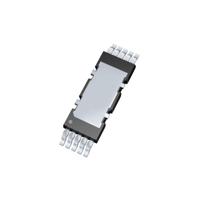
PG-HDSOP-10-1
CoolMOS™�is�a�revolutionary�technology�for�high�voltage�power
MOSFETs,�designed�according�to�the�superjunction�(SJ)�principle�and
pioneered�by�Infineon�Technologies.�The�latest�CoolMOS™�CFD7�is�the
successor�to�the�CoolMOS™�CFD2�series�and�is�an�optimized�platform
tailored�to�target�soft�switching�applications�such�as�phase-shift�full-bridge
(ZVS)�and�LLC.�Resulting�from�reduced�gate�charge�(Qg),�best-in-class
reverse�recovery�charge�(Qrr)�and�improved�turn�off�behavior�CoolMOS™
CFD7�offers�highest�efficiency�in�resonant�topologies.�As�part�of�Infineon’s
fast�body�diode�portfolio,�this�new�product�series�blends�all�advantages�of
a�fast�switching�technology�together�with�superior�hard�commutation
robustness,�without�sacrificing�easy�implementation�in�the�design-in
process.
10
6
tab
Pin 1
5
Drain
Pin 6-10, tab
Features
•�Ultra-fast�body�diode
•�Low�gate�charge
•�Best-in-class�reverse�recovery�charge�(Qrr)
•�Improved�MOSFET�reverse�diode�dv/dt�and�diF/dt�ruggedness
•�Lowest�FOM�RDS(on)*Qg�and�RDS(on)*Eoss
•�Best-in-class�RDS(on)�in�SMD�and�THD�packages
Gate
Pin 1
Driver
Source
Pin 2
Power
Source
Pin 3,4,5
Benefits
•�Excellent�hard�commutation�ruggedness
•�Highest�reliability�for�resonant�topologies
•�Highest�efficiency�with�outstanding�ease-of-use�/�performance�tradeoff
•�Enabling�increased�power�density�solutions
Potential�applications
Suitable�for�Soft�Switching�topologies
Optimized�for�phase-shift�full-bridge�(ZVS),�LLC�Applications�–�Server,
Telecom,�EV�Charging
Product�validation
Fully�qualified�according�to�JEDEC�for�Industrial�Applications
Please�note:�The�source�and�sense�source�pins�are�not�exchangeable.
Their�exchange�might�lead�to�malfunction.�For�paralleling�4pin�MOSFET
devices�the�placement�of�the�gate�resistor�is�generally�recommended�to�be
on�the�Driver�Source�instead�of�the�Gate.
Table�1�����Key�Performance�Parameters
Parameter
Value
Unit
VDS @ Tj,max
650
V
RDS(on),max
170
mΩ
Qg,typ
23
nC
ID,pulse
42
A
Eoss @ 400V
2.6
µJ
Body diode diF/dt
1300
A/µs
Type�/�Ordering�Code
Package
IPDD60R170CFD7
PG-HDSOP-10
Final Data Sheet
Marking
60R170F7
1
Related�Links
see Appendix A
Rev.�2.0,��2020-09-16
�600V�CoolMOS™�CFD7�Power�Transistor
IPDD60R170CFD7
Table�of�Contents
Description . . . . . . . . . . . . . . . . . . . . . . . . . . . . . . . . . . . . . . . . . . . . . . . . . . . . . . . . . . . . . . . . . . . . . . . . . . . . . 1
Maximum ratings . . . . . . . . . . . . . . . . . . . . . . . . . . . . . . . . . . . . . . . . . . . . . . . . . . . . . . . . . . . . . . . . . . . . . . . . 3
Thermal characteristics . . . . . . . . . . . . . . . . . . . . . . . . . . . . . . . . . . . . . . . . . . . . . . . . . . . . . . . . . . . . . . . . . . . . 4
Electrical characteristics . . . . . . . . . . . . . . . . . . . . . . . . . . . . . . . . . . . . . . . . . . . . . . . . . . . . . . . . . . . . . . . . . . . 5
Electrical characteristics diagrams . . . . . . . . . . . . . . . . . . . . . . . . . . . . . . . . . . . . . . . . . . . . . . . . . . . . . . . . . . . 7
Test Circuits . . . . . . . . . . . . . . . . . . . . . . . . . . . . . . . . . . . . . . . . . . . . . . . . . . . . . . . . . . . . . . . . . . . . . . . . . . . 11
Package Outlines . . . . . . . . . . . . . . . . . . . . . . . . . . . . . . . . . . . . . . . . . . . . . . . . . . . . . . . . . . . . . . . . . . . . . . . 12
Appendix A . . . . . . . . . . . . . . . . . . . . . . . . . . . . . . . . . . . . . . . . . . . . . . . . . . . . . . . . . . . . . . . . . . . . . . . . . . . . 13
Revision History . . . . . . . . . . . . . . . . . . . . . . . . . . . . . . . . . . . . . . . . . . . . . . . . . . . . . . . . . . . . . . . . . . . . . . . . 14
Trademarks . . . . . . . . . . . . . . . . . . . . . . . . . . . . . . . . . . . . . . . . . . . . . . . . . . . . . . . . . . . . . . . . . . . . . . . . . . . 14
Disclaimer . . . . . . . . . . . . . . . . . . . . . . . . . . . . . . . . . . . . . . . . . . . . . . . . . . . . . . . . . . . . . . . . . . . . . . . . . . . . 14
Final Data Sheet
2
Rev.�2.0,��2020-09-16
�600V�CoolMOS™�CFD7�Power�Transistor
IPDD60R170CFD7
1�����Maximum�ratings
at�Tj�=�25°C,�unless�otherwise�specified
Table�2�����Maximum�ratings
Parameter
Symbol
Continuous drain current1)
Values
Unit
Note�/�Test�Condition
19
12
A
TC=25°C
TC=100°C
-
42
A
TC=25°C
-
-
49
mJ
ID=3.3A; VDD=50V; see table 10
EAR
-
-
0.24
mJ
ID=3.3A; VDD=50V; see table 10
Avalanche current, single pulse
IAS
-
-
3.3
A
-
MOSFET dv/dt ruggedness
dv/dt
-
-
120
V/ns
VDS=0...400V
Gate source voltage (static)
VGS
-20
-
20
V
static;
Gate source voltage (dynamic)
VGS
-30
-
30
V
AC (f>1 Hz)
Power dissipation
Ptot
-
-
137
W
TC=25°C
Storage temperature
Tstg
-55
-
150
°C
-
Operating junction temperature
Tj
-55
-
150
°C
-
-
-
-
n.a.
Ncm -
IS
-
-
19
A
TC=25°C
Diode pulse current
IS,pulse
-
-
42
A
TC=25°C
Reverse diode dv/dt3)
dv/dt
-
-
70
V/ns
VDS=0...400V,�ISD