Data Sheet No.PD 60155H
IPS511/IPS511S
FULLY PROTECTED HIGH SIDE POWER MOSFET SWITCH
Features
•
•
•
•
•
•
•
Product Summary
Over temperature protection (with auto-restart)
Short-circuit protection (current limit )
Active clamp
E.S.D protection
Status feedback
Open load detection
Logic ground isolated from power ground
Rds(on)
135mΩ (max)
V clamp
50V
I Limit
5A
V open load
3V
Description
The IPS511/IPS511S are fully protected five terminal
high side switches with built in short circuit, over-temperature, ESD protection, inductive load capability
and diagnostic feedback. The output current is controlled when it reaches I lim value. The current
limitation is activated until the thermal protection
acts. The over-temperature protection turns off the
high side switch if the junction temperature exceeds
Tshutdown. It will automatically restart after the junction has cooled 7 oC below Tshutdown. A diagnostic
pin is provided for status feedback of short-circuit,
over-temperature and open load detection. The double
level shifter circuitry allows large offsets between the
logic ground and the load ground.
Typical Connection
Truth Table
Op. Conditions
Normal
Normal
Open load
Open load
Over current
Over current
Over-temperature
Over-temperature
In
Out
H
H
L
L
H
H
L
H
H L (limiting)
L
L
H L (cycling)
L
L
Dg
H
L
H
H
L
L
L
L
Packages
+ VCC
+ 5v
15K
Status
feedback
Output pull-up resistor
Vcc
Dg
Logic
Rdg
Rin
Logic
signal
www.irf.com
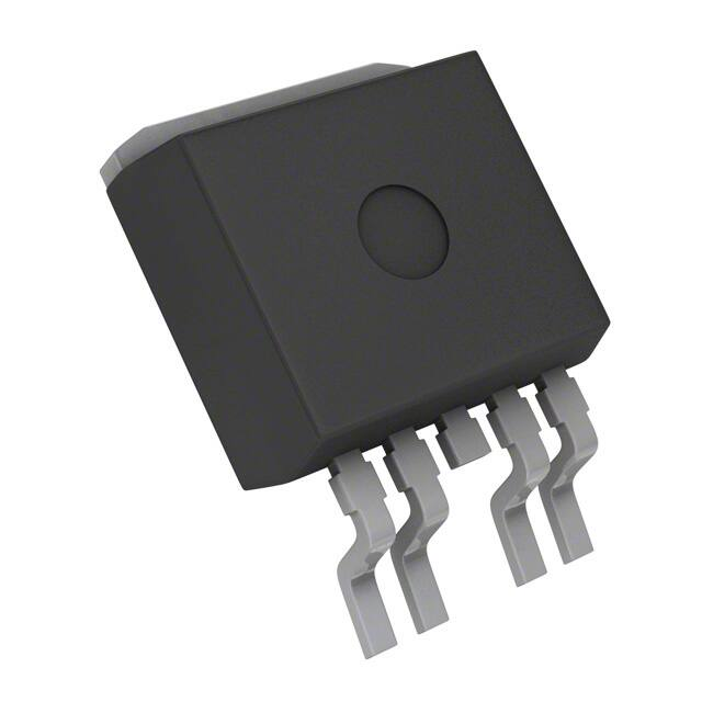
5 Lead
D2Pak (SMD220
IPS511S
control
Out
In
Gnd
Load
Logic Gnd
Load Gnd
5 Lead
TO220
IPS511
1
�IPS511/IPS511S
Absolute Maximum Ratings
Absolute maximum ratings indicate sustained limits beyond which damage to the device may occur. All voltage parameters
are referenced to GROUND lead. (Tj = 25oC unless otherwise specified).
Symbol Parameter
Min.
Vcc-50
Maximum logic ground to load ground offset Vcc-50
Max.
Units
Vout
Voffset
Maximum output voltage
Vin
Vcc max
Iin, max.
Maximum Input voltage
-0.3
5.5
Maximum Vcc voltage
Maximum IN current
—
-5
50
10
mA
Vdg
Idg, max
Maximum diagnostic output voltage
-0.3
5.5
V
mA
Test Conditions
Vcc+0.3
Vcc+0.3
Maximum diagnostic output current
Isd cont. Diode max. permanent current (1)
Isd pulsed Diode max. pulsed current (1)
-1
10
—
2.2
—
10
ESD1
Electrostatic discharge voltage (Human Body)
—
4
ESD2
Electrostatic discharge voltage (Machine Model)
—
0.5
V
A
C=100pF, R=1500Ω,
kV
C=200pF, R=0Ω, L=10µH
(1)
Pd
Maximum power dissipation
(TC=25oC) IPS511
(rth=80 oC/W) IPS511S
—
25
—
1.56
Tj max.
Max. storage & operating junction temp.
-40
+150
Tlead
Lead temperature (soldering 10 seconds)
—
300
Min.
Typ.
—
—
—
—
—
#
W
o
C
Thermal Characteristics
Symbol Parameter
Rth
Rth
Rth
Rth
Rth
1
2
1
2
3
Thermal
Thermal
Thermal
Thermal
Thermal
resistance
resistance
resistance
resistance
resistance
junction to case
junction to ambient
with standard footprint
with 1" square footprint
junction to case
$�
60
40
#
Max. Units Test Conditions
—
—
—
—
—
TO-220
o
C/W
D2PAK (SMD220)
(1) Limited by junction temperature (pulsed current limited also by internal wiring)
2
www.irf.com
�IPS511/IPS511S
Recommended Operating Conditions
These values are given for a quick design. For operation outside these conditions, please consult the application notes.
Symbol Parameter
Min.
Max.
Vcc
VIH
VIL
Iout
5.5
4
-0.3
35
5.5
0.9
—
—
4
10
1.7
1.5
6
20
Continuous Vcc voltage
High level input voltage
Low level input voltage
Continuous output current
Tamb=85 oC
(TAmbient = 85oC, Tj = 125oC, Rth < 60oC/W) IPS511
(TAmbient = 85oC, Tj = 125oC, Rth = 80oC/W) IPS511
Rin
Recommended resistor in series with IN pin
Rdg
Recommended resistor in series with DG pin
Units
V
A
kΩ
Static Electrical Characteristics
(Tj = 25oC, Vcc = 14V unless otherwise specified.)
Symbol Parameter
Min.
Typ.
ON state resistance Tj = 25oC
—
110
135
ON state resistance @ Vcc = 6V
—
110
135
ON state resistance Tj = 150oC
—
200
—
Vcc oper.
V clamp 1
V clamp 2
Vf
Icc off
Icc on
Icc ac
Vdgl
Ioh
Iol
Idg
Operating voltage range
Vcc to OUT clamp voltage 1
Vcc to OUT clamp voltage 2
Body diode forward voltage
Supply current when OFF
Supply current when ON
Ripple current when ON (AC RMS)
Low level diagnostic output voltage
Output leakage current
Output leakage current
5.5
50
—
—
—
—
—
—
—
0
—
56
58
0.9
16
0.7
20
0.15
60
—
35
—
65
1.2
50
2
—
0.4
110
25
leakage
Diagnostic output leakage current
IN high threshold voltage
IN low threshold voltage
On state IN positive current
Input hysteresis
—
—
1
—
0.1
—
2.3
1.95
70
0.25
10
3
—
200
0.5
Rds(on)
Max. Units Test Conditions
Vin = 5V, Iout = 2.5A
@Tj=25o C
Rds(on)
(V cc=6V)
Rds(on)
mΩ
Vin = 5V, Iout = 1A
Vin = 5V, Iout = 2.5A
@Tj=150oC
Vih
Vil
Iin, on
In hyst.
www.irf.com
V
µA
mA
µA
V
µA
Id = 10mA (see Fig.1 & 2)
Id = Isd (see Fig.1 & 2)
Id = 2.5A, Vin = 0V
Vin = 0V, Vout = 0V
Vin = 5V
Vin = 5V
Idg = 1.6 mA
Vout = 6V
Vout = 0V
Vdg = 5.5V
V
µA
V
Vin = 5V
3
�IPS511/IPS511S
Switching Electrical Characteristics
Vcc = 14V, Resistive Load = 5.6Ω, Tj = 25oC, (unless otherwise specified).
�Symbol Parameter
Min.
Tdon
Turn-on delay time
Tr1
Rise time to Vout = Vcc - 5V
Tr2
Rise time Vcc - 5V to Vout = 90% of Vcc
dV/dt (on) Turn ON dV/dt
E on
Turn ON energy
T doff
Turn-off delay time
Tf
Fall time to Vout = 10% of Vcc
dV/dt (off) Turn OFF dV/dt
Eoff
Turn OFF energy
Tdiag
Vout to Vdiag propagation delay
Typ. Max. Units Test Conditions
—
—
—
—
—
—
—
—
—
—
7
10
45
1.3
400
15
10
2
80
5
Min.
Typ.
3
—
—
2
2
5
165
158
3
3
50
50
100
4
—
50
50
6
—
15
µs
See figure 3
V/µs
µJ
µs
V/µs
µJ
µs
See figure 4
See figure 6
Protection Characteristics
Symbol Parameter
Ilim
Internal current limit
T sd+
Over-temp. positive going threshold
TsdOver-temp. negative going threshold
V sc
Short-circuit detection voltage (3)
Vopen load Open load detection threshold
Max. Units Test Conditions
7
—
—
4
4
A
C
o
C
V
V
o
Vout = 0V
See fig. 2
See fig. 2
See fig. 2
(3) Referenced to Vcc
Lead Assignments
3 (Vcc)
3 (Vcc)
1 - Ground
2 - In
3 - Vcc
4 - DG
5 - Out
12345
12345
5 Lead - D2PAK (SMD220)
5 Lead - TO220
IPS511
IPS511S
Part Number
4
www.irf.com
�IPS511/IPS511S
Functional Block Diagram
All values are typical
VCC
50V
Over
temperature
165°C
158°C
Tj
Charge
pump
62 V
2.7 V
IN
Level
shift
2.2 V
7 V
200 KΩ
driver
Current
limit
DG
+
5A
7 V
20 Ω
3V
+
+
Short-circuit
Open load
GND
3V
-
VOUT
T clamp
Vin
5V
0V
Vin
Iout
limiting
T shutdown
cycling
Ilim.
Iout
( + Vcc )
0V
Out
T
V clamp
Tsd+
Tsd(160 ° )
( see Appl . Notes to evaluate power dissipation )
Figure 1 - Active clamp waveforms
www.irf.com
Figure 2 - Protection timing diagram
5
�IPS511/IPS511S
Vin
Vcc
90%
Vin
Vcc - 5V
Vout
dV/dt on
90%
10%
Td on
dV/dt off
Tr 1
Vout
Tr 2
E1(t)
10%
Iout1
Eon1
Iout2
Resistive load
Td off
E2 (t)
Tf
Inductive load
Eon2
Figure 4 - Switching times definition (turn-off)
Figure 3 - Switching times definition (turn-on)
Turn on energy with a resistive or an
inductive load
V in
Dg Vcc
Vcc
Vcc -Vsc
IN
Out
+
Gnd
L
Vin
14 V
V o ut
Vout
Vol
R
V d ia g
5v
0v
Iout
Diag off blanking
Diag on blanking
Rem :
V load is negative during demagnetization
Figure 5 - Active clamp test circuit
6
T diag
Figure 6 - Diagnostic delay definitions
www.irf.com
�IPS511/IPS511S
150
2 00 %
100
1 50 %
50
1 00 %
0
5 0%
0
5
10
15
20
25
30
-5 0
35
0
50
100
150
Figure 8 - Normalized Rds(on) (%) Vs Tj (oC)
Figure 7 - Rds(on) (mΩ) Vs Vcc (V)
150
10
100
1
50
0.1
0
0
1
2
3
4
Figure 9 - Rds(on) (mΩ) Vs Iout (A)
www.irf.com
5
Figure 10 - Max. Iout (A) Vs Load Inductance (uH)
7
�IPS511/IPS511S
5
5
Rthja= 20°C/W
Rthja= 10°C/W
4
4
1inch² footprint
Rthja= 35°C/W
Rthja= 40°C/W
3
3
Free air
2
2
1
1
0
Std. footprint
Rthja= 60°C/W
0
25
50
75
100
125
150
Figure 11a - Max load current (A) Vs Tamb (oC)
IPS511
1 00
25
50
75
100
125
150
Figure 11b - Max load current (A) Vs Tamb (oC)
IPS511S
6
5
10
4
1
3
2
0 .1
1
0 .0 1
0
-50
Figure 12 - Transient Thermal Impedance (oC/W)
Vs Time (S)
8
0
50
100
150
Figure 13 - Ilim (A) Vs Tj (oC)
www.irf.com
�IPS511/IPS511S
Resistive load
600
10000
1000
I=Imax vs Induct.(see fig.10)
Eon
400
Eoff
100
I=1.5A
10
200
Figure 14 - Eon, Eoff (µJ) (A) Vs Iout (A)
0.1
1E+06
3
1E+05
2
1E+04
1
1E+03
0
1E+02
0
1E+01
1
Figure 15 - Eon (µJ) Vs Load Inductance (µH)
(see Fig. 3)
150
1.00E-03
125
Diag on blanking
100
1.00E-04
75
50
1.00E-05
25
Diag off blanking
0
0
1
2
Figure 16 - Diag Blanking time (µS) Vs Iout (A)
(resistive load - see Fig. 6)
www.irf.com
3
1.00E-06
0
5
10
15
20
25
30
35
Figure 17 - Icc (mA) Vs Vcc (V)
9
�IPS511/IPS511S
150
125
100
75
50
25
0
-50 -25
0
25
50
75 100 125 150
Figure 18 - Iin @ Vin = 5V (µA) Vs Tj (oC)
Case Outline 5 Lead - TO220
IRGB 01-3042 01
10
www.irf.com
�IPS511/IPS511S
Case Outline 5 Lead - D2PAK (SMD220)
01-3066 00
www.irf.com
11
�IPS511/IPS511S
Tape & Reel
5 Lead - D2PAK (SMD220)
01-3071 00 / 01-3072 00
IR WORLD HEADQUARTERS: 233 Kansas St., El Segundo, California 90245 Tel: (310) 252-7105
IR EUROPEAN REGIONAL CENTRE: 439/445 Godstone Rd., Whyteleafe, Surrey CR3 0BL, United Kingdom
Tel: ++ 44 (0) 20 8645 8000
IR JAPAN: K&H Bldg., 2F, 30-4 Nishi-Ikebukuro 3-Chome, Toshima-Ku, Tokyo, Japan 171-0021 Tel: 8133 983 0086
IR HONG KONG: Unit 308, #F, New East Ocean Centre, No. 9 Science Museum Road, Tsimshatsui East, Kowloon
Hong Kong Tel: (852) 2803-7380
Data and specifications subject to change without notice. 3/27/2000
12
www.irf.com
�Note: For the most current drawings please refer to the IR website at:
http://www.irf.com/package/
�
很抱歉,暂时无法提供与“IPS511STRL”相匹配的价格&库存,您可以联系我们找货
免费人工找货