MOSFET
Metal�Oxide�Semiconductor�Field�Effect�Transistor
OptiMOSTM
OptiMOSTM�Power-Transistor,�60�V
IPT007N06N
Data�Sheet
Rev.�2.1
Final
Power�Management�&�Multimarket
�OptiMOSTM�Power-Transistor,�60�V
IPT007N06N
1�����Description
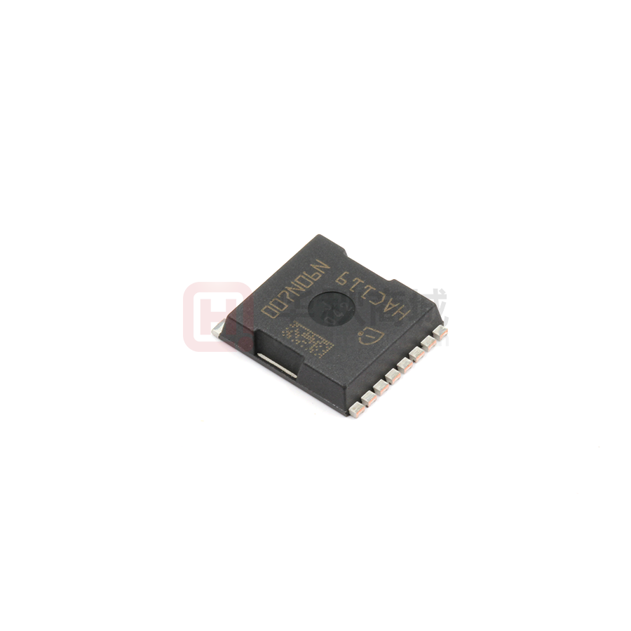
HSOF
Features
Tab
•�100%�avalanche�tested
•�Superior�thermal�resistance
•�N-channel
•�Qualified�according�to�JEDEC�1)��for�target�applications
•�Pb-free�lead��plating;�RoHS�compliant
•�Halogen-free�according�to�IEC61249-2-21
12
34
56
78
Table�1�����Key�Performance�Parameters
Parameter
Value
Unit
VDS
60
V
RDS(on),max
0.75
mΩ
ID
300
A
Qoss
227
nC
QG(0V..10V)
216
nC
Drain
Tab
Gate
Pin 1
Source
Pin 2-8
Type�/�Ordering�Code
Package
Marking
Related�Links
IPT007N06N
PG-HSOF-8-1
007N06N
-
1)
J-STD20 and JESD22
Final Data Sheet
2
Rev.�2.1,��2014-02-20
�OptiMOSTM�Power-Transistor,�60�V
IPT007N06N
Table�of�Contents
Description . . . . . . . . . . . . . . . . . . . . . . . . . . . . . . . . . . . . . . . . . . . . . . . . . . . . . . . . . . . . . . . . . . . . . . . . . . . . . 2
Maximum ratings . . . . . . . . . . . . . . . . . . . . . . . . . . . . . . . . . . . . . . . . . . . . . . . . . . . . . . . . . . . . . . . . . . . . . . . . 4
Thermal characteristics . . . . . . . . . . . . . . . . . . . . . . . . . . . . . . . . . . . . . . . . . . . . . . . . . . . . . . . . . . . . . . . . . . . . 4
Electrical characteristics . . . . . . . . . . . . . . . . . . . . . . . . . . . . . . . . . . . . . . . . . . . . . . . . . . . . . . . . . . . . . . . . . . . 5
Electrical characteristics diagrams . . . . . . . . . . . . . . . . . . . . . . . . . . . . . . . . . . . . . . . . . . . . . . . . . . . . . . . . . . . 7
Package Outlines . . . . . . . . . . . . . . . . . . . . . . . . . . . . . . . . . . . . . . . . . . . . . . . . . . . . . . . . . . . . . . . . . . . . . . . 11
Revision History . . . . . . . . . . . . . . . . . . . . . . . . . . . . . . . . . . . . . . . . . . . . . . . . . . . . . . . . . . . . . . . . . . . . . . . . 12
Disclaimer . . . . . . . . . . . . . . . . . . . . . . . . . . . . . . . . . . . . . . . . . . . . . . . . . . . . . . . . . . . . . . . . . . . . . . . . . . . . 12
Final Data Sheet
3
Rev.�2.1,��2014-02-20
�OptiMOSTM�Power-Transistor,�60�V
IPT007N06N
2�����Maximum�ratings
at�Tj�=�25�°C,�unless�otherwise�specified
Table�2�����Maximum�ratings
Parameter
Symbol
Values
Unit
Note�/�Test�Condition
Min.
Typ.
Max.
-
-
300
300
52
A
ID,pulse
-
-
1200
A
TC=25�°C
EAS
-
-
1100
mJ
ID=150�A,�RGS=25�Ω
Gate source voltage
VGS
-20
-
20
V
-
Power dissipation
Ptot
-
-
375
W
TC=25�°C
Operating and storage temperature
Tj,�Tstg
-55
-
175
°C
IEC climatic category;
DIN IEC 68-1: 55/175/56
Unit
Note�/�Test�Condition
ID
Continuous drain current
Pulsed drain current 2)
Avalanche energy, single pulse
3)
VGS=10�V,�TC=25�°C
VGS=10�V,�TC=100�°C
VGS=10�V,�TC=25�°C,�RthJA�=40�K/W
1)
3�����Thermal�characteristics
Table�3�����Thermal�characteristics
Parameter
Symbol
Thermal resistance, junction - case
Values
Min.
Typ.
Max.
RthJC
-
0.2
0.4
K/W
-
Device on PCB, minimal footprint
RthJA
-
-
62
K/W
-
Device on PCB, 6 cm² cooling area 1)
RthJA
-
-
40
K/W
-
1)
Device on 40 mm x 40 mm x 1.5 mm epoxy PCB FR4 with 6 cm2 (one layer, 70 µm thick) copper area for drain
connection. PCB is vertical in still air.
2)
See figure 3 for more detailed information
3)
See figure 13 for more detailed information
Final Data Sheet
4
Rev.�2.1,��2014-02-20
�OptiMOSTM�Power-Transistor,�60�V
IPT007N06N
4�����Electrical�characteristics
Table�4�����Static�characteristics
Parameter
Symbol
Drain-source breakdown voltage
Values
Unit
Note�/�Test�Condition
-
V
VGS=0�V,�ID=1�mA
2.8
3.3
V
VDS=VGS,�ID=280�µA
-
0.5
10
1
100
µA
VDS=60�V,�VGS=0�V,�Tj=25�°C
VDS=60�V,�VGS=0�V,�Tj=125�°C
IGSS
-
10
100
nA
VGS=20�V,�VDS=0�V
Drain-source on-state resistance
RDS(on)
-
0.66
0.85
0.75
1
mΩ
VGS=10�V,�ID=150�A
VGS=6�V,�ID=75�A
Gate resistance
RG
-
1.8
2.7
Ω
-
Transconductance
gfs
160
320
-
S
|VDS|>2|ID|RDS(on)max,�ID=100�A
Unit
Note�/�Test�Condition
Min.
Typ.
Max.
V(BR)DSS
60
-
Gate threshold voltage
VGS(th)
2.1
Zero gate voltage drain current
IDSS
Gate-source leakage current
Table�5�����Dynamic�characteristics
Parameter
Symbol
Input capacitance
Values
Min.
Typ.
Max.
Ciss
-
16000 21280 pF
VGS=0�V,�VDS=30�V,�f=1�MHz
Output capacitance
Coss
-
3400
4522
pF
VGS=0�V,�VDS=30�V,�f=1�MHz
Reverse transfer capacitance
Crss
-
229
458
pF
VGS=0�V,�VDS=30�V,�f=1�MHz
Turn-on delay time
td(on)
-
38
-
ns
VDD=30�V,�VGS=10�V,�ID=100�A,
RG,ext=1.8�Ω
Rise time
tr
-
18
-
ns
VDD=30�V,�VGS=10�V,�ID=100�A,
RG,ext=1.8�Ω
Turn-off delay time
td(off)
-
76
-
ns
VDD=30�V,�VGS=10�V,�ID=100�A,
RG,ext=1.8�Ω
Fall time
tf
-
22
-
ns
VDD=30�V,�VGS=10�V,�ID=100�A,
RG,ext=1.8�Ω
Unit
Note�/�Test�Condition
Table�6�����Gate�charge�characteristics�1)�
Parameter
Symbol
Gate to source charge
Values
Min.
Typ.
Max.
Qgs
-
67
-
nC
VDD=30�V,�ID=100�A,�VGS=0�to�10�V
Gate charge at threshold
Qg(th)
-
47
-
nC
VDD=30�V,�ID=100�A,�VGS=0�to�10�V
Gate to drain charge
Qgd
-
39
-
nC
VDD=30�V,�ID=100�A,�VGS=0�to�10�V
Switching charge
Qsw
-
58
-
nC
VDD=30�V,�ID=100�A,�VGS=0�to�10�V
Gate charge total
Qg
-
216
287
nC
VDD=30�V,�ID=100�A,�VGS=0�to�10�V
Gate plateau voltage
Vplateau
-
4.2
-
V
VDD=30�V,�ID=100�A,�VGS=0�to�10�V
Gate charge total, sync. FET
Qg(sync)
-
192
255
nC
VDS=0.1�V,�VGS=0�to�10�V
Output charge
Qoss
-
227
-
-
VDD=30�V,�VGS=0�V
1)
See ″Gate charge waveforms″ for parameter definition
Final Data Sheet
5
Rev.�2.1,��2014-02-20
�OptiMOSTM�Power-Transistor,�60�V
IPT007N06N
Table�7�����Reverse�diode
Parameter
Symbol
Diode continuous forward current
Values
Unit
Note�/�Test�Condition
300
A
TC=25�°C
-
1200
A
TC=25�°C
-
0.87
1
V
VGS=0�V,�IF=150�A,�Tj=25�°C
trr
-
87
174
ns
VR=30�V,�IF=100A,�diF/dt=100�A/µs
Qrr
-
144
-
nC
VR=30�V,�IF=100A,�diF/dt=100�A/µs
Min.
Typ.
Max.
IS
-
-
Diode pulse current
IS,pulse
-
Diode forward voltage
VSD
Reverse recovery time
Reverse recovery charge
Final Data Sheet
6
Rev.�2.1,��2014-02-20
�OptiMOSTM�Power-Transistor,�60�V
IPT007N06N
5�����Electrical�characteristics�diagrams
Diagram�1:�Power�dissipation
Diagram�2:�Drain�current
400
350
350
300
300
250
200
ID�[A]
Ptot�[W]
250
200
150
150
100
100
50
50
0
0
25
50
75
100
125
150
0
175
0
25
50
75
TC�[°C]
100
125
150
175
200
TC�[°C]
Ptot=f(TC)
ID=f(TC);�VGS≥10�V
Diagram�3:�Safe�operating�area
Diagram�4:�Max.�transient�thermal�impedance
4
100
10
1 µs
103
10 µs
0.5
10-1
ID�[A]
102
0.2
ZthJC�[K/W]
100 µs
1 ms
1
10
10 ms
0.1
0.05
0.02
10-2
0.01
DC
100
single pulse
10-1
10-1
100
101
102
10-3
10-6
10-5
10-4
VDS�[V]
10-2
10-1
100
tp�[s]
ID=f(VDS);�TC=25�°C;�D=0;�parameter:�tp
Final Data Sheet
10-3
ZthJC=f(tp);�parameter:�D=tp/T
7
Rev.�2.1,��2014-02-20
�OptiMOSTM�Power-Transistor,�60�V
IPT007N06N
Diagram�5:�Typ.�output�characteristics
Diagram�6:�Typ.�drain-source�on�resistance
1200
3.0
10 V
6V
7V
1000
2.5
800
2.0
RDS(on)��[mΩ]
ID�[A]
5.5 V
600
400
5V
1.5
5.5 V
6V
1.0
5V
7V
200
0
10 V
0.5
0.0
0.5
1.0
1.5
2.0
2.5
0.0
3.0
0
200
400
VDS�[V]
600
800
1000
1200
ID�[A]
ID=f(VDS);�Tj=25�°C;�parameter:�VGS
RDS(on)=f(ID);�Tj=25�°C;�parameter:�VGS
Diagram�7:�Typ.�transfer�characteristics
Diagram�8:�Typ.�forward�transconductance
1200
450
400
1000
350
300
gfs�[S]
ID�[A]
800
600
400
250
200
150
100
200
50
175 °C
0
0
2
25 °C
4
6
8
0
0
VGS�[V]
100
150
200
ID�[A]
ID=f(VGS);�|VDS|>2|ID|RDS(on)max;�parameter:�Tj
Final Data Sheet
50
gfs=f(ID);�Tj=25�°C
8
Rev.�2.1,��2014-02-20
�OptiMOSTM�Power-Transistor,�60�V
IPT007N06N
Diagram�9:�Drain-source�on-state�resistance
Diagram�10:�Typ.�gate�threshold�voltage
1.6
4
1.2
3
2800 µA
VGS(th)�[V]
RDS(on)�[mΩ]
280 µA
max
0.8
typ
0.4
2
1
0.0
-60
-20
20
60
100
140
0
-60
180
-20
20
Tj�[°C]
60
100
140
180
Tj�[°C]
RDS(on)=f(Tj);�ID=150�A;�VGS=10�V
VGS(th)=f(Tj);�VGS=VDS
Diagram�11:�Typ.�capacitances
Diagram�12:�Forward�characteristics�of�reverse�diode
5
104
10
25 °C
175 °C
25 °C, 98%
175 °C, 98%
Ciss
103
Coss
IF�[A]
C�[pF]
104
3
10
Crss
102
101
0
20
102
101
40
60
100
0.0
0.5
VDS�[V]
C=f(VDS);�VGS=0�V;�f=1�MHz
Final Data Sheet
1.0
1.5
2.0
VSD�[V]
IF=f(VSD);�parameter:�Tj
9
Rev.�2.1,��2014-02-20
�OptiMOSTM�Power-Transistor,�60�V
IPT007N06N
Diagram�13:�Avalanche�characteristics
Diagram�14:�Typ.�gate�charge
103
12
30 V
10
12 V
48 V
125 °C
100 °C
8
25 °C
IAV�[A]
VGS�[V]
102
101
6
4
2
100
100
101
102
103
0
0
50
tAV�[µs]
100
150
200
250
Qgate�[nC]
IAS=f(tAV);�RGS=25�Ω;�parameter:�Tj(start)
VGS=f(Qgate);�ID=100�A�pulsed;�parameter:�VDD
Diagram�15:�Drain-source�breakdown�voltage
Gate charge waveforms
68
66
64
VBR(DSS)�[V]
62
60
58
56
54
52
-60
-20
20
60
100
140
180
Tj�[°C]
VBR(DSS)=f(Tj);�ID=1�mA
Final Data Sheet
10
Rev.�2.1,��2014-02-20
�OptiMOSTM�Power-Transistor,�60�V
IPT007N06N
6�����Package�Outlines
1) partially covered with Mold Flash
DIM
A
b
b1
b2
c
D
D2
E
E1
E4
E5
e
H
H1
H2
H3
H4
N
K1
L
L1
L2
L4
MILLIMETERS
MIN
MAX
2.20
2.40
0.70
0.90
9.70
9.90
0.42
0.50
0.40
0.60
10.28
10.58
3.30
9.70
10.10
7.50
8.50
9.46
1.20 (BSC)
11.48
6.55
11.88
6.75
INCHES
MIN
0.087
0.028
0.382
0.017
0.016
0.405
0.295
0.335
0.372
0.047 (BSC)
0.452
0.258
2
0
2
4mm
EUROPEAN PROJECTION
0.083
ISSUE DATE
20-02-2014
0.051
REVISION
02
0.028
0.024
1.30
0
SCALE
0.468
0.266
0.063
0.70
0.60
1.00
0.398
0.281
0.141
0.128
8
0.165
2.10
DOCUMENT NO.
Z8B00169619
0.130
0.382
7.15
3.59
3.26
8
4.18
1.60
MAX
0.094
0.035
0.390
0.020
0.024
0.416
0.039
Figure�1�����Outline�PG-HSOF-8-1,�dimensions�in�mm/inches
Final Data Sheet
11
Rev.�2.1,��2014-02-20
�OptiMOSTM�Power-Transistor,�60�V
IPT007N06N
Revision�History
IPT007N06N
Revision:�2014-02-20,�Rev.�2.1
Previous Revision
Revision
Date
Subjects (major changes since last revision)
2.0
2014-02-06
Release of final version
2.1
2014-02-20
Update Diagram 12
We�Listen�to�Your�Comments
Any�information�within�this�document�that�you�feel�is�wrong,�unclear�or�missing�at�all?�Your�feedback�will�help�us�to�continuously
improve�the�quality�of�this�document.�Please�send�your�proposal�(including�a�reference�to�this�document)�to:
erratum@infineon.com
Published�by
Infineon�Technologies�AG
81726�München,�Germany
©�2014�Infineon�Technologies�AG
All�Rights�Reserved.
Legal�Disclaimer
The�information�given�in�this�document�shall�in�no�event�be�regarded�as�a�guarantee�of�conditions�or�characteristics.�With
respect�to�any�examples�or�hints�given�herein,�any�typical�values�stated�herein�and/or�any�information�regarding�the�application
of�the�device,�Infineon�Technologies�hereby�disclaims�any�and�all�warranties�and�liabilities�of�any�kind,�including�without
limitation,�warranties�of�non-infringement�of�intellectual�property�rights�of�any�third�party.
Information
For�further�information�on�technology,�delivery�terms�and�conditions�and�prices�please�contact�your�nearest�Infineon
Technologies�Office�(www.infineon.com).
Warnings
Due�to�technical�requirements,�components�may�contain�dangerous�substances.�For�information�on�the�types�in�question,
please�contact�the�nearest�Infineon�Technologies�Office.
The�Infineon�Technologies�component�described�in�this�Data�Sheet�may�be�used�in�life-support�devices�or�systems�and/or
automotive,�aviation�and�aerospace�applications�or�systems�only�with�the�express�written�approval�of�Infineon�Technologies,�if�a
failure�of�such�components�can�reasonably�be�expected�to�cause�the�failure�of�that�life-support,�automotive,�aviation�and
aerospace�device�or�system�or�to�affect�the�safety�or�effectiveness�of�that�device�or�system.�Life�support�devices�or�systems�are
intended�to�be�implanted�in�the�human�body�or�to�support�and/or�maintain�and�sustain�and/or�protect�human�life.�If�they�fail,�it�is
reasonable�to�assume�that�the�health�of�the�user�or�other�persons�may�be�endangered.
Final Data Sheet
12
Rev.�2.1,��2014-02-20
�