IPT111N20NFD
MOSFET
OptiMOSª3�Power-Transistor,�200�V
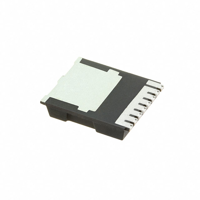
HSOF
Features
Tab
•�N-channel,�normal�level
•�Fast�Diode�(FD)�with�reduced�Qrr
•�Optimized�for�hard�commutation�ruggedness
•�Very�low�on-resistance�RDS(on)
•�175�°C�operating�temperature
•�Pb-free�lead�plating;�RoHS�compliant
•�Qualified�according�to�JEDEC1)��for�target�application
•�Halogen-free�according�to�IEC61249-2-21
12
34
56
78
Table�1�����Key�Performance�Parameters
Parameter
Value
Unit
VDS
200
V
RDS(on),max
11.1
mΩ
ID
96
A
Type�/�Ordering�Code
Package
IPT111N20NFD
PG-HSOF-8
1)
Drain
Tab
Gate
Pin 1
Source
Pin 2-8
Marking
111N20NF
Related�Links
-
J-STD20 and JESD22
Final Data Sheet
1
Rev.�2.1,��2016-02-23
�OptiMOSª3�Power-Transistor,�200�V
IPT111N20NFD
Table�of�Contents
Description . . . . . . . . . . . . . . . . . . . . . . . . . . . . . . . . . . . . . . . . . . . . . . . . . . . . . . . . . . . . . . . . . . . . . . . . . . . . . 1
Maximum ratings . . . . . . . . . . . . . . . . . . . . . . . . . . . . . . . . . . . . . . . . . . . . . . . . . . . . . . . . . . . . . . . . . . . . . . . . 3
Thermal characteristics . . . . . . . . . . . . . . . . . . . . . . . . . . . . . . . . . . . . . . . . . . . . . . . . . . . . . . . . . . . . . . . . . . . . 3
Electrical characteristics . . . . . . . . . . . . . . . . . . . . . . . . . . . . . . . . . . . . . . . . . . . . . . . . . . . . . . . . . . . . . . . . . . . 3
Electrical characteristics diagrams . . . . . . . . . . . . . . . . . . . . . . . . . . . . . . . . . . . . . . . . . . . . . . . . . . . . . . . . . . . 5
Package Outlines . . . . . . . . . . . . . . . . . . . . . . . . . . . . . . . . . . . . . . . . . . . . . . . . . . . . . . . . . . . . . . . . . . . . . . . . 9
Revision History . . . . . . . . . . . . . . . . . . . . . . . . . . . . . . . . . . . . . . . . . . . . . . . . . . . . . . . . . . . . . . . . . . . . . . . . 10
Trademarks . . . . . . . . . . . . . . . . . . . . . . . . . . . . . . . . . . . . . . . . . . . . . . . . . . . . . . . . . . . . . . . . . . . . . . . . . . . 10
Disclaimer . . . . . . . . . . . . . . . . . . . . . . . . . . . . . . . . . . . . . . . . . . . . . . . . . . . . . . . . . . . . . . . . . . . . . . . . . . . . 10
Final Data Sheet
2
Rev.�2.1,��2016-02-23
�OptiMOSª3�Power-Transistor,�200�V
IPT111N20NFD
1�����Maximum�ratings
at�TA=25�°C,�unless�otherwise�specified
Table�2�����Maximum�ratings
Parameter
Symbol
Continuous drain current
Values
Unit
Note�/�Test�Condition
96
76
A
TC=25�°C
TC=100�°C
-
384
A
TC=25�°C
-
-
375
mJ
ID=67�A,�RGS=25�Ω
VGS
-20
-
20
V
-
Power dissipation
Ptot
-
-
375
W
TC=25�°C
Operating and storage temperature
Tj,�Tstg
-55
-
175
°C
IEC climatic category;
DIN IEC 68-1: 55/175/56
Unit
Note�/�Test�Condition
Min.
Typ.
Max.
ID
-
-
Pulsed drain current1)
ID,pulse
-
Avalanche energy, single pulse
EAS
Gate source voltage
2�����Thermal�characteristics
Table�3�����Thermal�characteristics
Parameter
Symbol
Thermal resistance, junction - case
Values
Min.
Typ.
Max.
RthJC
-
-
0.4
K/W
-
Thermal resistance, junction - ambient,
RthJA
minimal footprint
-
-
62
K/W
-
Thermal resistance, junction - ambient,
RthJA
6 cm2 cooling area2)
-
-
40
K/W
-
Unit
Note�/�Test�Condition
3�����Electrical�characteristics
Table�4�����Static�characteristics
Parameter
Symbol
Drain-source breakdown voltage
Values
Min.
Typ.
Max.
V(BR)DSS
200
-
-
V
VGS=0�V,�ID=1�mA
Gate threshold voltage
VGS(th)
2
3
4
V
VDS=VGS,�ID=267�µA
Zero gate voltage drain current
IDSS
-
0.1
10
1
100
µA
VDS=160�V,�VGS=0�V,�Tj=25�°C
VDS=160�V,�VGS=0�V,�Tj=125�°C
Gate-source leakage current
IGSS
-
1
100
nA
VGS=20�V,�VDS=0�V
Drain-source on-state resistance
RDS(on)
-
9
11.1
mΩ
VGS=10�V,�ID=96�A
Gate resistance
RG
-
2.8
4.2
Ω
-
Transconductance
gfs
82
163
-
S
|VDS|>2|ID|RDS(on)max,�ID=96�A
3)
1)
See Diagram 3
Device on 40 mm x 40 mm x 1.5 mm epoxy PCB FR4 with 6 cm2 (one layer, 70 µm thick) copper area for drain connection.
PCB is vertical in still air.
3)
Defined by design. Not subject to production test
2)
Final Data Sheet
3
Rev.�2.1,��2016-02-23
�OptiMOSª3�Power-Transistor,�200�V
IPT111N20NFD
Table�5�����Dynamic�characteristics1)�
Parameter
Symbol
Input capacitance
Values
Unit
Note�/�Test�Condition
7000
pF
VGS=0�V,�VDS=100�V,�f=1�MHz
400
530
pF
VGS=0�V,�VDS=100�V,�f=1�MHz
-
6
9.4
pF
VGS=0�V,�VDS=100�V,�f=1�MHz
td(on)
-
13
-
ns
VDD=100�V,�VGS=10�V,�ID=48�A,
RG,ext=1.6�Ω
Rise time
tr
-
11
-
ns
VDD=100�V,�VGS=10�V,�ID=48�A,
RG,ext=1.6�Ω
Turn-off delay time
td(off)
-
39
-
ns
VDD=100�V,�VGS=10�V,�ID=48�A,
RG,ext=1.6�Ω
Fall time
tf
-
13
-
ns
VDD=100�V,�VGS=10�V,�ID=48�A,
RG,ext=1.6�Ω
Unit
Note�/�Test�Condition
Min.
Typ.
Max.
Ciss
-
5300
Output capacitance
Coss
-
Reverse transfer capacitance
Crss
Turn-on delay time
Table�6�����Gate�charge�characteristics2)�
Parameter
Symbol
Values
Min.
Typ.
Max.
Qgs
-
25
-
nC
VDD=100�V,�ID=96�A,�VGS=0�to�10�V
Gate to drain charge
Qgd
-
8
-
nC
VDD=100�V,�ID=96�A,�VGS=0�to�10�V
Switching charge
Qsw
-
17
-
nC
VDD=100�V,�ID=96�A,�VGS=0�to�10�V
Gate charge total
Qg
-
65
87
nC
VDD=100�V,�ID=96�A,�VGS=0�to�10�V
Gate plateau voltage
Vplateau
-
4.7
-
V
VDD=100�V,�ID=96�A,�VGS=0�to�10�V
Qoss
-
162
-
nC
VDD=100�V,�VGS=0�V
Unit
Note�/�Test�Condition
Gate to source charge
1)
1)
1)
Output charge
Table�7�����Reverse�diode
Parameter
Symbol
Diode continous forward current
Diode pulse current
Diode forward voltage
1)
Reverse recovery time
1)
Reverse recovery charge
1)
2)
Values
Min.
Typ.
Max.
IS
-
-
96
A
TC=25�°C
IS,pulse
-
-
384
A
TC=25�°C
VSD
-
0.95
1.2
V
VGS=0�V,�IF=96�A,�Tj=25�°C
trr
-
125
250
ns
VR=100�V,�IF=IS,�diF/dt=100�A/µs
Qrr
-
309
-
nC
VR=100�V,�IF=IS,�diF/dt=100�A/µs
Defined by design. Not subject to production test
See ″Gate charge waveforms″ for parameter definition
Final Data Sheet
4
Rev.�2.1,��2016-02-23
�OptiMOSª3�Power-Transistor,�200�V
IPT111N20NFD
4�����Electrical�characteristics�diagrams
Diagram�1:�Power�dissipation
Diagram�2:�Drain�current
400
100
350
80
300
60
ID�[A]
Ptot�[W]
250
200
40
150
100
20
50
0
0
50
100
150
0
200
0
50
100
TC�[°C]
150
200
TC�[°C]
Ptot=f(TC)
ID=f(TC);�VGS≥10�V
Diagram�3:�Safe�operating�area
Diagram�4:�Max.�transient�thermal�impedance
3
100
10
1 µs
10 µs
2
10
100 µs
0.5
ZthJC�[K/W]
ID�[A]
1 ms
10 ms
101
DC
10-1
0.2
0.1
0.05
100
0.02
0.01
single pulse
-1
10
10-1
100
101
102
103
10
-2
10-5
10-4
VDS�[V]
10-2
10-1
100
tp�[s]
ID=f(VDS);�TC=25�°C;�D=0;�parameter:�tp
Final Data Sheet
10-3
ZthJC=f(tp);�parameter:�D=tp/T
5
Rev.�2.1,��2016-02-23
�OptiMOSª3�Power-Transistor,�200�V
IPT111N20NFD
Diagram�5:�Typ.�output�characteristics
Diagram�6:�Typ.�drain-source�on�resistance
350
30
10 V
8V
300
7V
6.5 V
6V
250
20
5.5 V
ID�[A]
RDS(on)��[mΩ]
200
150
5V
4.5 V
5V
5.5 V
6V
10
8V
100
10 V
4.5 V
50
0
0
1
2
3
4
0
5
0
50
VDS�[V]
100
150
ID�[A]
ID=f(VDS);�Tj=25�°C;�parameter:�VGS
RDS(on)=f(ID);�Tj=25�°C;�parameter:�VGS
Diagram�7:�Typ.�transfer�characteristics
Diagram�8:�Typ.�forward�transconductance
200
220
200
180
150
160
gfs�[S]
ID�[A]
140
100
120
100
80
25 °C
175 °C
50
60
40
20
0
0
2
4
6
8
0
0
VGS�[V]
80
120
160
ID�[A]
ID=f(VGS);�|VDS|>2|ID|RDS(on)max;�parameter:�Tj
Final Data Sheet
40
gfs=f(ID);�Tj=25�°C
6
Rev.�2.1,��2016-02-23
�OptiMOSª3�Power-Transistor,�200�V
IPT111N20NFD
Diagram�9:�Drain-source�on-state�resistance
Diagram�10:�Typ.�gate�threshold�voltage
40
4.0
3.5
30
2670 µA
3.0
267 µA
VGS(th)�[V]
RDS(on)�[mΩ]
2.5
20
2.0
1.5
98%
typ
10
1.0
0.5
0
-60
-20
20
60
100
140
0.0
-60
180
-20
20
Tj�[°C]
60
100
140
180
Tj�[°C]
RDS(on)=f(Tj);�ID=96�A;�VGS=10�V
VGS(th)=f(Tj);�VGS=VDS;�parameter:�ID
Diagram�11:�Typ.�capacitances
Diagram�12:�Forward�characteristics�of�reverse�diode
4
103
10
Ciss
25 °C
175 °C
25°C, 98%
175°C, 98%
103
Coss
IF�[A]
C�[pF]
102
102
101
101
100
Crss
0
20
40
60
80
100
120
140
160
100
0.0
0.5
VDS�[V]
C=f(VDS);�VGS=0�V;�f=1�MHz
Final Data Sheet
1.0
1.5
2.0
VSD�[V]
IF=f(VSD);�parameter:�Tj
7
Rev.�2.1,��2016-02-23
�OptiMOSª3�Power-Transistor,�200�V
IPT111N20NFD
Diagram�13:�Avalanche�characteristics
Diagram�14:�Typ.�gate�charge
3
10
10
8
160 V
102
100 V
6
40 V
VGS�[V]
IAS�[A]
25 °C
100 °C
125 °C
4
1
10
2
100
100
101
102
103
0
0
tAV�[µs]
20
40
60
80
Qgate�[nC]
IAS=f(tAV);�RGS=25�Ω;�parameter:�Tj(start)
VGS=f(Qgate);�ID=96�A�pulsed;�parameter:�VDD
Diagram�15:�Drain-source�breakdown�voltage
Gate charge waveforms
230
220
VBR(DSS)�[V]
210
200
190
180
-60
-20
20
60
100
140
180
Tj�[°C]
VBR(DSS)=f(Tj);�ID=1�mA
Final Data Sheet
8
Rev.�2.1,��2016-02-23
�OptiMOSª3�Power-Transistor,�200�V
IPT111N20NFD
5�����Package�Outlines
1) partially covered with Mold Flash
DIM
A
b
b1
b2
c
D
D2
E
E1
E4
E5
e
H
H1
H2
H3
H4
N
K1
L
L1
L2
L4
MILLIMETERS
MIN
MAX
2.20
2.40
0.70
0.90
9.70
9.90
0.42
0.50
0.40
0.60
10.28
10.58
3.30
9.70
10.10
7.50
8.50
9.46
1.20 (BSC)
11.48
6.55
11.88
6.75
INCHES
MIN
0.087
0.028
0.382
0.017
0.016
0.405
MAX
0.094
0.035
0.390
0.020
0.024
0.416
0.398
0.295
0.335
0.372
0.047 (BSC)
0.452
0.258
EUROPEAN PROJECTION
0.063
0.083
ISSUE DATE
20-02-2014
0.051
REVISION
02
0.028
0.024
1.30
2
0.468
0.266
0.70
0.60
1.00
2
0
4mm
0.281
0.141
0.128
8
0.165
2.10
0
SCALE
0.130
0.382
7.15
3.59
3.26
8
4.18
1.60
DOCUMENT NO.
Z8B00169619
0.039
Figure�1�����Outline�PG-HSOF-8
Final Data Sheet
9
Rev.�2.1,��2016-02-23
�OptiMOSª3�Power-Transistor,�200�V
IPT111N20NFD
Revision�History
IPT111N20NFD
Revision:�2016-02-23,�Rev.�2.1
Previous Revision
Revision
Date
Subjects (major changes since last revision)
2.0
2016-01-11
Release of final version
2.1
2016-02-23
Update Eas and Vds for Idss
Trademarks�of�Infineon�Technologies�AG
AURIX™,�C166™,�CanPAK™,�CIPOS™,�CoolGaN™,�CoolMOS™,�CoolSET™,�CoolSiC™,�CORECONTROL™,�CROSSAVE™,�DAVE™,�DI-POL™,�DrBlade™,
EasyPIM™,�EconoBRIDGE™,�EconoDUAL™,�EconoPACK™,�EconoPIM™,�EiceDRIVER™,�eupec™,�FCOS™,�HITFET™,�HybridPACK™,�Infineon™,
ISOFACE™,�IsoPACK™,�i-Wafer™,�MIPAQ™,�ModSTACK™,�my-d™,�NovalithIC™,�OmniTune™,�OPTIGA™,�OptiMOS™,�ORIGA™,�POWERCODE™,
PRIMARION™,�PrimePACK™,�PrimeSTACK™,�PROFET™,�PRO-SIL™,�RASIC™,�REAL3™,�ReverSave™,�SatRIC™,�SIEGET™,�SIPMOS™,�SmartLEWIS™,
SOLID�FLASH™,�SPOC™,�TEMPFET™,�thinQ�™,�TRENCHSTOP™,�TriCore™.
Trademarks�updated�August�2015
Other�Trademarks
All�referenced�product�or�service�names�and�trademarks�are�the�property�of�their�respective�owners.
We�Listen�to�Your�Comments
Any�information�within�this�document�that�you�feel�is�wrong,�unclear�or�missing�at�all?�Your�feedback�will�help�us�to�continuously
improve�the�quality�of�this�document.�Please�send�your�proposal�(including�a�reference�to�this�document)�to:
erratum@infineon.com
Published�by
Infineon�Technologies�AG
81726�München,�Germany
©�2015�Infineon�Technologies�AG
All�Rights�Reserved.
Legal�Disclaimer
The�information�given�in�this�document�shall�in�no�event�be�regarded�as�a�guarantee�of�conditions�or�characteristics.�With
respect�to�any�examples�or�hints�given�herein,�any�typical�values�stated�herein�and/or�any�information�regarding�the�application
of�the�device,�Infineon�Technologies�hereby�disclaims�any�and�all�warranties�and�liabilities�of�any�kind,�including�without
limitation,�warranties�of�non-infringement�of�intellectual�property�rights�of�any�third�party.
Information
For�further�information�on�technology,�delivery�terms�and�conditions�and�prices�please�contact�your�nearest�Infineon
Technologies�Office�(www.infineon.com).
Warnings
Due�to�technical�requirements,�components�may�contain�dangerous�substances.�For�information�on�the�types�in�question,
please�contact�the�nearest�Infineon�Technologies�Office.
The�Infineon�Technologies�component�described�in�this�Data�Sheet�may�be�used�in�life-support�devices�or�systems�and/or
automotive,�aviation�and�aerospace�applications�or�systems�only�with�the�express�written�approval�of�Infineon�Technologies,�if�a
failure�of�such�components�can�reasonably�be�expected�to�cause�the�failure�of�that�life-support,�automotive,�aviation�and
aerospace�device�or�system�or�to�affect�the�safety�or�effectiveness�of�that�device�or�system.�Life�support�devices�or�systems�are
intended�to�be�implanted�in�the�human�body�or�to�support�and/or�maintain�and�sustain�and/or�protect�human�life.�If�they�fail,�it�is
reasonable�to�assume�that�the�health�of�the�user�or�other�persons�may�be�endangered.
Final Data Sheet
10
Rev.�2.1,��2016-02-23
�