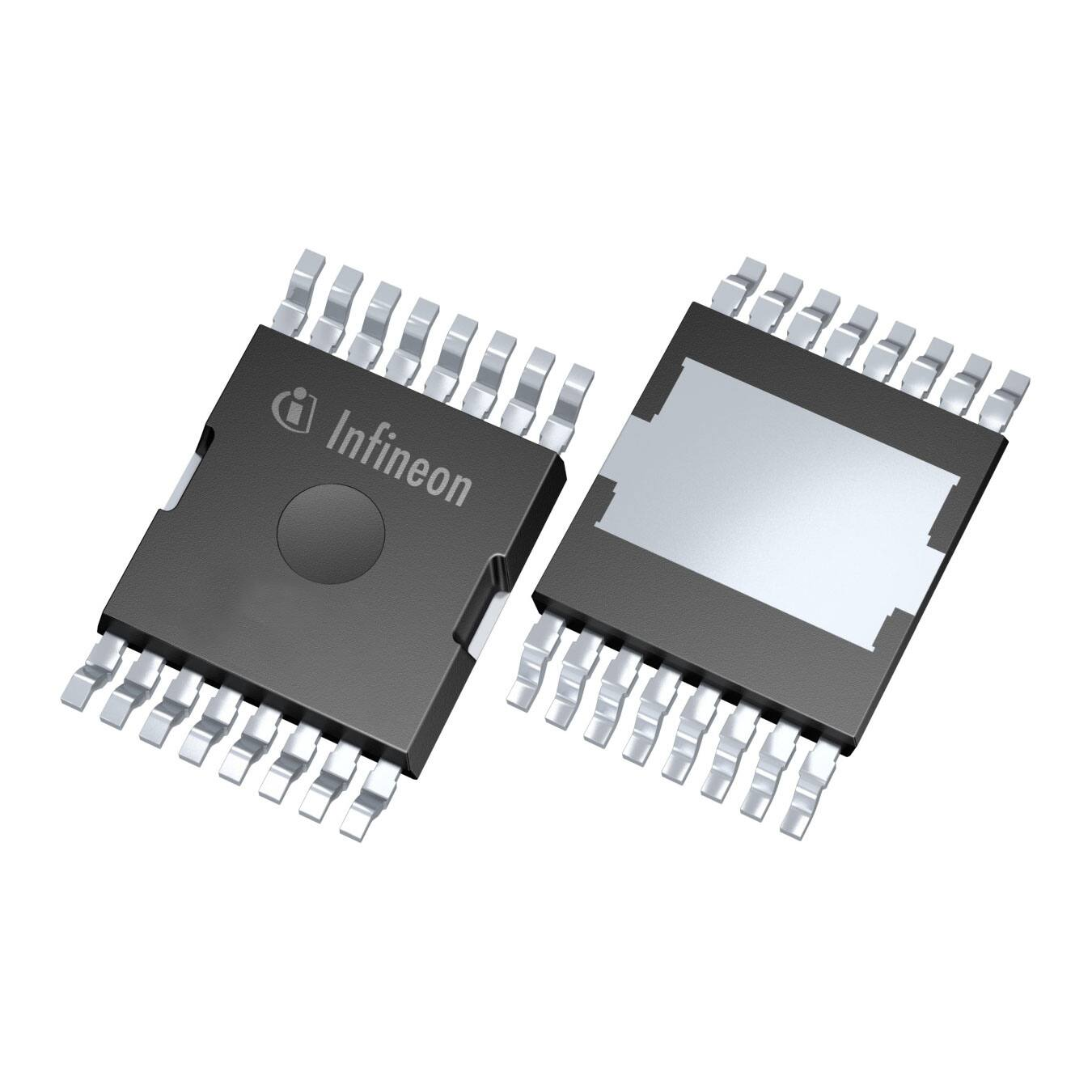
IPTC012N08NM5
MOSFET
OptiMOSTM�5�Power-Transistor,�80�V
PG-HDSOP-16-2
16
Features
16
9
9
•�Optimized�for�motor�drives�and�battery�powered�applications
•�Optimized�for�top�side�cooling
•�High�current�capability
•�175°C�rated
•�100%�avalanche�tested
•�Superior�thermal�performance
•�N-channel
•�Pb-free�lead�plating;�RoHS�compliant
•�Halogen-free�according�to�IEC61249-2-21
1
8
8
1
Product�validation
Drain
Pin 9-16, Tab
Fully�qualified�according�to�JEDEC�for�Industrial�Applications
Gate
Pin 8
Table�1�����Key�Performance�Parameters
Parameter
Value
Unit
VDS
80
V
RDS(on),max
1.2
mΩ
ID
396
A
Qoss
204
nC
QG
175
nC
Type�/�Ordering�Code
Package
IPTC012N08NM5
PG-HDSOP-16
Final Data Sheet
Source
Pin 1-7
Marking
12N08NM5
1
Related�Links
-
Rev.�2.0,��2021-02-02
�OptiMOSTM�5�Power-Transistor,�80�V
IPTC012N08NM5
Table�of�Contents
Description . . . . . . . . . . . . . . . . . . . . . . . . . . . . . . . . . . . . . . . . . . . . . . . . . . . . . . . . . . . . . . . . . . . . . . . . . . . . . 1
Maximum ratings . . . . . . . . . . . . . . . . . . . . . . . . . . . . . . . . . . . . . . . . . . . . . . . . . . . . . . . . . . . . . . . . . . . . . . . . 3
Thermal characteristics . . . . . . . . . . . . . . . . . . . . . . . . . . . . . . . . . . . . . . . . . . . . . . . . . . . . . . . . . . . . . . . . . . . . 3
Electrical characteristics . . . . . . . . . . . . . . . . . . . . . . . . . . . . . . . . . . . . . . . . . . . . . . . . . . . . . . . . . . . . . . . . . . . 4
Electrical characteristics diagrams . . . . . . . . . . . . . . . . . . . . . . . . . . . . . . . . . . . . . . . . . . . . . . . . . . . . . . . . . . . 6
Package Outlines . . . . . . . . . . . . . . . . . . . . . . . . . . . . . . . . . . . . . . . . . . . . . . . . . . . . . . . . . . . . . . . . . . . . . . . 10
Revision History . . . . . . . . . . . . . . . . . . . . . . . . . . . . . . . . . . . . . . . . . . . . . . . . . . . . . . . . . . . . . . . . . . . . . . . . 11
Trademarks . . . . . . . . . . . . . . . . . . . . . . . . . . . . . . . . . . . . . . . . . . . . . . . . . . . . . . . . . . . . . . . . . . . . . . . . . . . 11
Disclaimer . . . . . . . . . . . . . . . . . . . . . . . . . . . . . . . . . . . . . . . . . . . . . . . . . . . . . . . . . . . . . . . . . . . . . . . . . . . . 11
Final Data Sheet
2
Rev.�2.0,��2021-02-02
�OptiMOSTM�5�Power-Transistor,�80�V
IPTC012N08NM5
1�����Maximum�ratings
at�TA=25�°C,�unless�otherwise�specified
Table�2�����Maximum�ratings
Parameter
Symbol
Values
Unit
Note�/�Test�Condition
396
283
231
40
A
VGS=10�V,�TC=25�°C
VGS=10�V,�TC=100�°C
VGS=6�V,�TC=100�°C
VGS=10�V,TA=25°C,RthJA=40°C/W2)
-
1584
A
TA=25�°C
-
-
817
mJ
ID=150�A,�RGS=25�Ω
VGS
-20
-
20
V
-
Power dissipation
Ptot
-
-
375
3.8
W
TC=25�°C
TA=25�°C,�RthJA=40�°C/W2)
Operating and storage temperature
Tj,�Tstg
-55
-
175
°C
IEC climatic category; DIN IEC 68-1:
55/175/56
Unit
Note�/�Test�Condition
Min.
Typ.
Max.
ID
-
-
ID,pulse
-
Avalanche energy, single pulse
EAS
Gate source voltage
1)
Continuous drain current
Pulsed drain current3)
4)
2�����Thermal�characteristics
Table�3�����Thermal�characteristics
Parameter
Symbol
Thermal resistance, junction - case,
Top
Values
Min.
Typ.
Max.
RthJC
-
-
0.4
°C/W -
Thermal characterization parameter,
junction to lead (Pin 1-7)5)
ΨJL
-
9
-
°C/W -
Thermal characterization parameter,
junction to lead (Pin 9-16)5)
ΨJL
-
3
-
°C/W -
-
40
-
°C/W -
Thermal resistance, junction - ambient RthJA
1)
Rating refers to the product only with datasheet specified absolute maximum values, maintaining case temperature
as specified. For other case temperatures please refer to Diagram 2. De-rating will be required based on the actual
environmental conditions.
2)
Device on 40 mm x 40 mm x 1.5 mm epoxy PCB FR4 with 6 cm2 (one layer, 70 µm thick) copper area for drain
connection. PCB is vertical in still air.
3)
See Diagram 3 for more detailed information
4)
See Diagram 13 for more detailed information
5)
ΨJL is a temperature characterization parameter according to JESD51-12 referring to the temperature difference between
junction and leads in the case of natural convection. It can be used to estimate the component junction temperature in the
application by measuring the temperature at the leads in the stated application environment
Final Data Sheet
3
Rev.�2.0,��2021-02-02
�OptiMOSTM�5�Power-Transistor,�80�V
IPTC012N08NM5
3�����Electrical�characteristics
at�Tj=25�°C,�unless�otherwise�specified
Table�4�����Static�characteristics
Parameter
Symbol
Drain-source breakdown voltage
Values
Unit
Note�/�Test�Condition
-
V
VGS=0�V,�ID=1�mA
3
3.8
V
VDS=VGS,�ID=275�µA
-
0.1
10
1
100
µA
VDS=80�V,�VGS=0�V,�Tj=25�°C
VDS=80�V,�VGS=0�V,�Tj=125�°C
IGSS
-
10
100
nA
VGS=20�V,�VDS=0�V
Drain-source on-state resistance
RDS(on)
-
1.0
1.4
1.2
1.8
mΩ
VGS=10�V,�ID=100�A
VGS=6�V,�ID=75�A
Gate resistance
RG
-
1.5
-
Ω
-
Transconductance
gfs
-
250
-
S
|VDS|≥2|ID|RDS(on)max,�ID=100�A
Unit
Note�/�Test�Condition
Min.
Typ.
Max.
V(BR)DSS
80
-
Gate threshold voltage
VGS(th)
2.2
Zero gate voltage drain current
IDSS
Gate-source leakage current
Table�5�����Dynamic�characteristics
Parameter
Symbol
Input capacitance1)
Values
Min.
Typ.
Ciss
-
12000 16000 pF
VGS=0�V,�VDS=40�V,�f=1�MHz
Coss
-
2000
2600
pF
VGS=0�V,�VDS=40�V,�f=1�MHz
Reverse transfer capacitance
Crss
-
85
150
pF
VGS=0�V,�VDS=40�V,�f=1�MHz
Turn-on delay time
td(on)
-
31
-
ns
VDD=40�V,�VGS=10�V,�ID=100�A,
RG,ext=3.5�Ω
Rise time
tr
-
19
-
ns
VDD=40�V,�VGS=10�V,�ID=100�A,
RG,ext=3.5�Ω
Turn-off delay time
td(off)
-
69
-
ns
VDD=40�V,�VGS=10�V,�ID=100�A,
RG,ext=3.5�Ω
Fall time
tf
-
55
-
ns
VDD=40�V,�VGS=10�V,�ID=100�A,
RG,ext=3.5�Ω
Unit
Note�/�Test�Condition
Output capacitance1)
1)
Max.
Table�6�����Gate�charge�characteristics2)�
Parameter
Symbol
Gate to source charge
Gate charge at threshold
Values
Min.
Typ.
Max.
Qgs
-
55
-
nC
VDD=40�V,�ID=100�A,�VGS=0�to�10�V
Qg(th)
-
37
-
nC
VDD=40�V,�ID=100�A,�VGS=0�to�10�V
Gate to drain charge
Qgd
-
37
56
nC
VDD=40�V,�ID=100�A,�VGS=0�to�10�V
Switching charge
Qsw
-
55
-
nC
VDD=40�V,�ID=100�A,�VGS=0�to�10�V
Gate charge total
Qg
-
175
219
nC
VDD=40�V,�ID=100�A,�VGS=0�to�10�V
Gate plateau voltage
Vplateau
-
4.5
-
V
VDD=40�V,�ID=100�A,�VGS=0�to�10�V
Output charge1)
Qoss
-
204
271
nC
VDS=40�V,�VGS=0�V
1)
1)
1)
2)
Defined by design. Not subject to production test.
See ″Gate charge waveforms″ for parameter definition
Final Data Sheet
4
Rev.�2.0,��2021-02-02
�OptiMOSTM�5�Power-Transistor,�80�V
IPTC012N08NM5
Table�7�����Reverse�diode
Parameter
Symbol
Diode continuous forward current
Values
Unit
Note�/�Test�Condition
300
A
TC=25�°C
-
1584
A
TC=25�°C
-
0.85
1
V
VGS=0�V,�IF=100�A,�Tj=25�°C
trr
-
86
-
ns
VR=40�V,�IF=50�A,�diF/dt=100�A/µs
Qrr
-
177
-
nC
VR=40�V,�IF=50�A,�diF/dt=100�A/µs
Min.
Typ.
Max.
IS
-
-
Diode pulse current
IS,pulse
-
Diode forward voltage
VSD
Reverse recovery time
Reverse recovery charge
Final Data Sheet
5
Rev.�2.0,��2021-02-02
�OptiMOSTM�5�Power-Transistor,�80�V
IPTC012N08NM5
4�����Electrical�characteristics�diagrams
Diagram�1:�Power�dissipation
Diagram�2:�Drain�current
400
500
350
400
300
300
ID�[A]
Ptot�[W]
250
200
200
150
100
100
50
0
0
25
50
75
100
125
150
175
0
200
0
25
50
75
TC�[°C]
100
125
150
175
200
TC�[°C]
Ptot=f(TC)
ID=f(TC);�VGS≥10�V
Diagram�3:�Safe�operating�area
Diagram�4:�Max.�transient�thermal�impedance
4
101
10
1 µs
103
100
10 µs
single pulse
0.01
0.02
0.05
0.1
0.2
0.5
100 µs
ID�[A]
ZthJC�[K/W]
102
101
10-1
1 ms
10 ms
10-2
0
10
10-1
DC
10-1
100
101
102
10-3
10-5
10-4
VDS�[V]
10-2
10-1
100
tp�[s]
ID=f(VDS);�TC=25�°C;�D=0;�parameter:�tp
Final Data Sheet
10-3
ZthJC=f(tp);�parameter:�D=tp/T
6
Rev.�2.0,��2021-02-02
�OptiMOSTM�5�Power-Transistor,�80�V
IPTC012N08NM5
Diagram�5:�Typ.�output�characteristics
Diagram�6:�Typ.�drain-source�on�resistance
1600
3.2
10 V
8V
7V
1400
2.8
6V
1200
2.4
1000
2.0
800
6V
600
RDS(on)��[mΩ]
ID�[A]
4.5 V
400
5V
1.6
7V
1.2
8V
10 V
0.8
5V
200
0.4
4.5 V
0
0
1
2
3
4
0.0
5
0
100
200
300
VDS�[V]
400
500
600
700
800
ID�[A]
ID=f(VDS),�Tj=25�°C;�parameter:�VGS
RDS(on)=f(ID),�Tj=25�°C;�parameter:�VGS
Diagram�7:�Typ.�transfer�characteristics
Diagram�8:�Typ.�drain-source�on�resistance
1500
3.2
2.8
1250
2.4
175 °C
1000
RDS(on)��[mΩ]
ID�[A]
2.0
750
1.6
1.2
500
0.8
250
175 °C
25 °C
0.4
25 °C
0
0
1
2
3
4
5
6
7
VGS�[V]
0
2
4
6
8
10
VGS�[V]
ID=f(VGS),�|VDS|>2|ID|RDS(on)max;�parameter:�Tj
Final Data Sheet
0.0
RDS(on)=f(VGS),�ID=100�A;�parameter:�Tj
7
Rev.�2.0,��2021-02-02
�OptiMOSTM�5�Power-Transistor,�80�V
IPTC012N08NM5
Diagram�9:�Normalized�drain-source�on�resistance
Diagram�10:�Typ.�gate�threshold�voltage
2.0
4.0
3.5
3.0
2.5
1.2
VGS(th)�[V]
RDS(on)�(normalized�to�25�°C)
1.6
0.8
2.0
2750 µA
1.5
275 µA
1.0
0.4
0.5
0.0
-80
-40
0
40
80
120
160
0.0
-80
200
-40
0
40
Tj�[°C]
80
120
160
200
Tj�[°C]
RDS(on)=f(Tj),�ID=100�A,�VGS=10�V
VGS(th=f(Tj),�VGS=VDS;�parameter:�ID
Diagram�11:�Typ.�capacitances
Diagram�12:�Forward�characteristics�of�reverse�diode
5
104
10
25 °C
25 °C, max
175 °C
175 °C, max
Ciss
104
Coss
103
IF�[A]
C�[pF]
103
102
102
Crss
101
0
10
20
30
40
50
60
70
80
101
0.00
0.25
VDS�[V]
0.75
1.00
1.25
1.50
VSD�[V]
C=f(VDS);�VGS=0�V;�f=1�MHz
Final Data Sheet
0.50
IF=f(VSD);�parameter:�Tj
8
Rev.�2.0,��2021-02-02
�OptiMOSTM�5�Power-Transistor,�80�V
IPTC012N08NM5
Diagram�13:�Avalanche�characteristics
Diagram�14:�Typ.�gate�charge
3
10
10
16 V
40 V
64 V
8
102
VGS�[V]
IAV�[A]
6
25 °C
100 °C
4
1
10
150 °C
2
100
100
101
102
103
tAV�[µs]
0
0
25
50
75
100
125
150
175
200
Qgate�[nC]
IAS=f(tAV);�RGS=25�Ω;�parameter:�Tj,start
VGS=f(Qgate),�ID=100�A�pulsed,�Tj=25�°C;�parameter:�VDD
Diagram�15:�Drain-source�breakdown�voltage
Diagram Gate charge waveforms
88
86
VBR(DSS)�[V]
84
82
80
78
76
-80
-40
0
40
80
120
160
200
Tj�[°C]
VBR(DSS)=f(Tj);�ID=1�mA
Final Data Sheet
9
Rev.�2.0,��2021-02-02
�OptiMOSTM�5�Power-Transistor,�80�V
IPTC012N08NM5
5�����Package�Outlines
PACKAGE - GROUP
NUMBER:
REVISION: 01
DIMENSIONS
A
A1
b
c
D
D1
E
E1
E2
e
e1
L
P
PG-HDSOP-16-U01
DATE: 18.12.2020
MILLIMETERS
MIN.
MAX.
2.25
2.35
0.01
0.16
0.60
0.80
0.40
0.60
9.70
10.10
8.20
8.40
14.80
15.20
10.00
10.30
5.57
5.77
1.20
8.40
1.40
1.60
2.90
3.10
Figure�1�����Outline�PG-HDSOP-16,�dimensions�in�mm
Final Data Sheet
10
Rev.�2.0,��2021-02-02
�OptiMOSTM�5�Power-Transistor,�80�V
IPTC012N08NM5
Revision�History
IPTC012N08NM5
Revision:�2021-02-02,�Rev.�2.0
Previous Revision
Revision
Date
Subjects (major changes since last revision)
2.0
2021-02-02
Release of final version
Trademarks
All�referenced�product�or�service�names�and�trademarks�are�the�property�of�their�respective�owners.
We�Listen�to�Your�Comments
Any�information�within�this�document�that�you�feel�is�wrong,�unclear�or�missing�at�all?�Your�feedback�will�help�us�to�continuously
improve�the�quality�of�this�document.�Please�send�your�proposal�(including�a�reference�to�this�document)�to:
erratum@infineon.com
Published�by
Infineon�Technologies�AG
81726�München,�Germany
©�2020�Infineon�Technologies�AG
All�Rights�Reserved.
Legal�Disclaimer
The�information�given�in�this�document�shall�in�no�event�be�regarded�as�a�guarantee�of�conditions�or�characteristics�
(“Beschaffenheitsgarantie”)�.
With�respect�to�any�examples,�hints�or�any�typical�values�stated�herein�and/or�any�information�regarding�the�application�of�the
product,�Infineon�Technologies�hereby�disclaims�any�and�all�warranties�and�liabilities�of�any�kind,�including�without�limitation
warranties�of�non-infringement�of�intellectual�property�rights�of�any�third�party.
In�addition,�any�information�given�in�this�document�is�subject�to�customer’s�compliance�with�its�obligations�stated�in�this
document�and�any�applicable�legal�requirements,�norms�and�standards�concerning�customer’s�products�and�any�use�of�the
product�of�Infineon�Technologies�in�customer’s�applications.
The�data�contained�in�this�document�is�exclusively�intended�for�technically�trained�staff.�It�is�the�responsibility�of�customer’s
technical�departments�to�evaluate�the�suitability�of�the�product�for�the�intended�application�and�the�completeness�of�the�product
information�given�in�this�document�with�respect�to�such�application.
Information
For�further�information�on�technology,�delivery�terms�and�conditions�and�prices�please�contact�your�nearest�Infineon
Technologies�Office�(www.infineon.com).
Warnings
Due�to�technical�requirements,�components�may�contain�dangerous�substances.�For�information�on�the�types�in�question,
please�contact�the�nearest�Infineon�Technologies�Office.
The�Infineon�Technologies�component�described�in�this�Data�Sheet�may�be�used�in�life-support�devices�or�systems�and/or
automotive,�aviation�and�aerospace�applications�or�systems�only�with�the�express�written�approval�of�Infineon�Technologies,�if�a
failure�of�such�components�can�reasonably�be�expected�to�cause�the�failure�of�that�life-support,�automotive,�aviation�and
aerospace�device�or�system�or�to�affect�the�safety�or�effectiveness�of�that�device�or�system.�Life�support�devices�or�systems�are
intended�to�be�implanted�in�the�human�body�or�to�support�and/or�maintain�and�sustain�and/or�protect�human�life.�If�they�fail,�it�is
reasonable�to�assume�that�the�health�of�the�user�or�other�persons�may�be�endangered.
Final Data Sheet
11
Rev.�2.0,��2021-02-02
�