IPW60R105CFD7
MOSFET
600V�CoolMOSª�CFD7�Power�Transistor
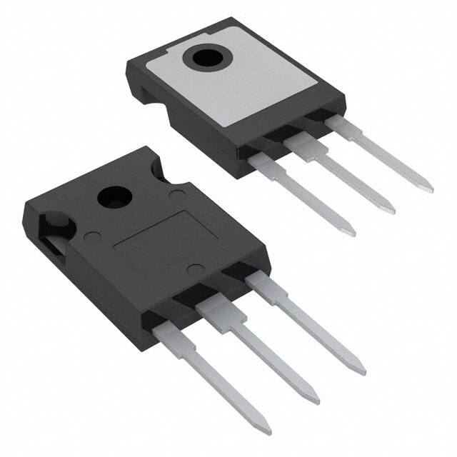
PG-TO�247-3
CoolMOS™�is�a�revolutionary�technology�for�high�voltage�power
MOSFETs,�designed�according�to�the�superjunction�(SJ)�principle�and
pioneered�by�Infineon�Technologies.�The�latest�CoolMOS™�CFD7�is�the
successor�to�the�CoolMOS™�CFD2�series�and�is�an�optimized�platform
tailored�to�target�soft�switching�applications�such�as�phase-shift�full-bridge
(ZVS)�and�LLC.�Resulting�from�reduced�gate�charge�(Qg),�best-in-class
reverse�recovery�charge�(Qrr)�and�improved�turn�off�behavior�CoolMOS™
CFD7�offers�highest�efficiency�in�resonant�topologies.�As�part�of�Infineon’s
fast�body�diode�portfolio,�this�new�product�series�blends�all�advantages�of
a�fast�switching�technology�together�with�superior�hard�commutation
robustness,�without�sacrificing�easy�implementation�in�the�design-in
process.�The�CoolMOS™�CFD7�technology�meets�highest�efficiency�and
reliability�standards�and�furthermore�supports�high�power�density
solutions.�Altogether,�CoolMOS™�CFD7�makes�resonant�switching
topologies�more�efficient,�more�reliable,�lighter�and�cooler.
Drain
Pin 2
Gate
Pin 1
Features
Source
Pin 3
•�Ultra-fast�body�diode
•�Low�gate�charge
•�Best-in-class�reverse�recovery�charge�(Qrr)
•�Improved�MOSFET�reverse�diode�dv/dt�and�diF/dt�ruggedness
•�Lowest�FOM�RDS(on)*Qg�and�RDS(on)*Eoss
•�Best-in-class�RDS(on)�in�SMD�and�THD�packages
Benefits
•�Excellent�hard�commutation�ruggedness
•�Highest�reliability�for�resonant�topologies
•�Highest�efficiency�with�outstanding�ease-of-use�/�performance�tradeoff
•�Enabling�increased�power�density�solutions
Potential�applications
Suiteable�for�Soft�Switching�topologies
Optimized�for�phase-shift�full-bridge�(ZVS),�LLC�Applications�–�Server,
Telecom,�EV�Charging
Product�Validation:�Qualified�for�industrial�applications�according�to�the
relevant�tests�of�JEDEC47/20/22
Please�note:�For�MOSFET�paralleling�the�use�of�ferrite�beads�on�the�gate
or�separate�totem�poles�is�generally�recommended.
Table�1�����Key�Performance�Parameters
Parameter
Value
Unit
VDS @ Tj,max
650
V
RDS(on),max
105
mΩ
Qg,typ
42
nC
ID,pulse
79
A
Eoss @ 400V
4.8
µJ
Body diode diF/dt
1300
A/µs
Type�/�Ordering�Code
Package
IPW60R105CFD7
PG-TO 247-3
Final Data Sheet
Marking
60R105F7
1
Related�Links
see Appendix A
Rev.�2.0,��2018-04-20
�600V�CoolMOSª�CFD7�Power�Transistor
IPW60R105CFD7
Table�of�Contents
Description . . . . . . . . . . . . . . . . . . . . . . . . . . . . . . . . . . . . . . . . . . . . . . . . . . . . . . . . . . . . . . . . . . . . . . . . . . . . . 1
Maximum ratings . . . . . . . . . . . . . . . . . . . . . . . . . . . . . . . . . . . . . . . . . . . . . . . . . . . . . . . . . . . . . . . . . . . . . . . . 3
Thermal characteristics . . . . . . . . . . . . . . . . . . . . . . . . . . . . . . . . . . . . . . . . . . . . . . . . . . . . . . . . . . . . . . . . . . . . 4
Electrical characteristics . . . . . . . . . . . . . . . . . . . . . . . . . . . . . . . . . . . . . . . . . . . . . . . . . . . . . . . . . . . . . . . . . . . 5
Electrical characteristics diagrams . . . . . . . . . . . . . . . . . . . . . . . . . . . . . . . . . . . . . . . . . . . . . . . . . . . . . . . . . . . 7
Test Circuits . . . . . . . . . . . . . . . . . . . . . . . . . . . . . . . . . . . . . . . . . . . . . . . . . . . . . . . . . . . . . . . . . . . . . . . . . . . 11
Package Outlines . . . . . . . . . . . . . . . . . . . . . . . . . . . . . . . . . . . . . . . . . . . . . . . . . . . . . . . . . . . . . . . . . . . . . . . 12
Appendix A . . . . . . . . . . . . . . . . . . . . . . . . . . . . . . . . . . . . . . . . . . . . . . . . . . . . . . . . . . . . . . . . . . . . . . . . . . . . 13
Revision History . . . . . . . . . . . . . . . . . . . . . . . . . . . . . . . . . . . . . . . . . . . . . . . . . . . . . . . . . . . . . . . . . . . . . . . . 14
Trademarks . . . . . . . . . . . . . . . . . . . . . . . . . . . . . . . . . . . . . . . . . . . . . . . . . . . . . . . . . . . . . . . . . . . . . . . . . . . 14
Disclaimer . . . . . . . . . . . . . . . . . . . . . . . . . . . . . . . . . . . . . . . . . . . . . . . . . . . . . . . . . . . . . . . . . . . . . . . . . . . . 14
Final Data Sheet
2
Rev.�2.0,��2018-04-20
�600V�CoolMOSª�CFD7�Power�Transistor
IPW60R105CFD7
1�����Maximum�ratings
at�Tj�=�25°C,�unless�otherwise�specified
Table�2�����Maximum�ratings
Parameter
Symbol
Continuous drain current1)
Values
Unit
Note�/�Test�Condition
21
13.0
A
TC=25°C
TC=100°C
-
79
A
TC=25°C
-
-
93
mJ
ID=4.8A; VDD=50V; see table 10
EAR
-
-
0.47
mJ
ID=4.8A; VDD=50V; see table 10
Avalanche current, single pulse
IAS
-
-
4.8
A
-
MOSFET dv/dt ruggedness
dv/dt
-
-
120
V/ns
VDS=0...400V
Gate source voltage (static)
VGS
-20
-
20
V
static;
Gate source voltage (dynamic)
VGS
-30
-
30
V
AC (f>1 Hz)
Power dissipation
Ptot
-
-
106
W
TC=25°C
Storage temperature
Tstg
-55
-
150
°C
-
Operating junction temperature
Tj
-55
-
150
°C
-
Mounting torque
-
-
-
60
Ncm M3 and M3.5 screws
IS
-
-
21
A
TC=25°C
Diode pulse current
IS,pulse
-
-
79
A
TC=25°C
Reverse diode dv/dt3)
dv/dt
-
-
70
V/ns
VDS=0...400V,�ISD
很抱歉,暂时无法提供与“IPW60R105CFD7XKSA1”相匹配的价格&库存,您可以联系我们找货
免费人工找货- 国内价格
- 1+37.53147
- 5+36.78168
- 10+34.05325
- 100+31.22069
- 250+28.88799
- 国内价格
- 30+21.35462
- 120+19.57489
- 国内价格 香港价格
- 1+46.505261+6.03288
- 10+33.9173710+4.39992
- 50+30.0710750+3.90096
- 100+28.23534100+3.66282
- 200+26.57444200+3.44736