Data Sheet No. PD60019 Rev.P
IR2130/IR2132(J)(S) & (PbF)
3-PHASE BRIDGE DRIVER
Features
• Floating channel designed for bootstrap operation
•
•
•
•
•
•
•
•
•
Fully operational to +600V
Tolerant to negative transient voltage
dV/dt immune
Gate drive supply range from 10 to 20V
Undervoltage lockout for all channels
Over-current shutdown turns off all six drivers
Independent half-bridge drivers
Matched propagation delay for all channels
2.5V logic compatible
Outputs out of phase with inputs
Cross-conduction prevention logic
Also available LEAD-FREE
Description
Product Summary
VOFFSET
600V max.
IO+/-
200 mA / 420 mA
VOUT
10 - 20V
ton/off (typ.)
675 & 425 ns
Deadtime (typ.)
2.5 µs (IR2130)
0.8 µs (IR2132)
Packages
The IR2130/IR2132(J)(S) is a high voltage, high speed
power MOSFET and IGBT driver with three independent high and low side referenced output channels. Proprietary HVIC technology enables ruggedized
28-Lead SOIC
monolithic construction. Logic inputs are compatible with
CMOS or LSTTL outputs, down to 2.5V logic. A
28-Lead PDIP
ground-referenced operational amplifier provides
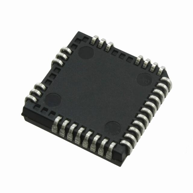
analog feedback of bridge current via an external current sense resistor. A current trip function which termi44-Lead PLCC w/o 12 Leads
nates all six outputs is also derived from this resistor.
An open drain FAULT signal indicates if an over-current or undervoltage shutdown has occurred. The output drivers feature a high pulse current buffer stage designed
for minimum driver cross-conduction. Propagation delays are matched to simplify use at high frequencies. The
floating channels can be used to drive N-channel power MOSFETs or IGBTs in the high side configuration
which operate up to 600 volts.
Typical Connection
(Refer to Lead Assignments for correct pin configuration). This/These diagram(s) show electrical connections only. Please refer
to our Application Notes and DesignTips for proper circuit board layout.
www.irf.com
1
�IR2130/IR2132(J)(S) & (PbF)
Absolute Maximum Ratings
Absolute Maximum Ratings indicate sustained limits beyond which damage to the device may occur. All voltage parameters are absolute voltages referenced to VS0. The Thermal Resistance and Power Dissipation ratings are measured
under board mounted and still air conditions. Additional information is shown in Figures 50 through 53.
Symbol
VB1,2,3
VS1,2,3
VHO1,2,3
VCC
VSS
VLO1,2,3
VIN
VFLT
VCAO
VCAdVS/dt
PD
RthJA
TJ
TS
TL
Definition
High Side Floating Supply Voltage
High Side Floating Offset Voltage
High Side Floating Output Voltage
Low Side and Logic Fixed Supply Voltage
Logic Ground
Low Side Output Voltage
Logic Input Voltage ( HIN1,2,3 , LIN1,2,3 & ITRIP)
FAULT Output Voltage
Operational Amplifier Output Voltage
Operational Amplifier Inverting Input Voltage
Allowable Offset Supply Voltage Transient
Package Power Dissipation @ TA ≤ +25°C
Thermal Resistance, Junction to Ambient
(28 Lead DIP)
(28 Lead SOIC)
(44 Lead PLCC)
(28 Lead DIP)
(28 Lead SOIC)
(44 Lead PLCC)
Junction Temperature
Storage Temperature
Lead Temperature (Soldering, 10 seconds)
Min.
Max.
-0.3
VB1,2,3 - 25
VS1,2,3 - 0.3
-0.3
VCC - 25
-0.3
VSS - 0.3
625
VB1,2,3 + 0.3
VB1,2,3 + 0.3
25
VCC + 0.3
VCC + 0.3
(V SS + 15) or
(VCC + 0.3)
whichever is
lower
VCC + 0.3
VCC + 0.3
VCC + 0.3
50
1.5
1.6
2.0
83
78
63
150
150
300
VSS - 0.3
VSS - 0.3
VSS - 0.3
—
—
—
—
—
—
—
—
-55
—
Units
V
V/ns
W
°C/W
°C
Recommended Operating Conditions
The Input/Output logic timing diagram is shown in Figure 1. For proper operation the device should be used within the
recommended conditions. All voltage parameters are absolute voltages referenced to VS0. The VS offset rating is tested
with all supplies biased at 15V differential. Typical ratings at other bias conditions are shown in Figure 54.
Symbol
Definition
Min.
Max.
Units
VB1,2,3
High Side Floating Supply Voltage
VS1,2,3 + 10
VS1,2,3 + 20
VS1,2,3
High Side Floating Offset Voltage
Note 1
600
VHO1,2,3
High Side Floating Output Voltage
VS1,2,3
VB1,2,3
VCC
Low Side and Logic Fixed Supply Voltage
10
20
VSS
Logic Ground
-5
5
VLO1,2,3
Low Side Output Voltage
0
VCC
V
VIN
Logic Input Voltage ( HIN1,2,3 , LIN1,2,3 & ITRIP)
VSS
VSS + 5
VFLT
VSS
VCC
FAULT Output Voltage
VCAO
Operational Amplifier Output Voltage
VSS
VSS + 5
VCAOperational Amplifier Inverting Input Voltage
VSS
VSS + 5
TA
Ambient Temperature
-40
125
°C
Note 1: Logic operational for VS of (VS0 - 5V) to (VS0 + 600V). Logic state held for VS of (VS0 - 5V) to (VS0 - VBS).
(Please refer to the Design Tip DT97-3 for more details).
Note 2: All input pins, CA- and CAO pins are internally clamped with a 5.2V zener diode.
2
www.irf.com
�IR2130/IR2132(J)(S) & (PbF)
Dynamic Electrical Characteristics
VBIAS (VCC, VBS1,2,3) = 15V, VS0,1,2,3 = VSS, CL = 1000 pF and TA = 25°C unless otherwise specified. The dynamic
electrical characteristics are defined in Figures 3 through 5.
Symbol
Definition
ton
toff
tr
tf
titrip
tbl
tflt
tflt,in
tfltclr
DT
Turn-On Propagation Delay
Turn-Off Propagation Delay
Turn-On Rise Time
Turn-Off Fall Time
ITRIP to Output Shutdown Prop. Delay
ITRIP Blanking Time
ITRIP to FAULT Indication Delay
Input Filter Time (All Six Inputs)
LIN1,2,3 to FAULT Clear Time
Deadtime
(IR2130)
(IR2132)
Operational Amplifier Slew Rate (+)
Operational Amplifier Slew Rate (-)
SR+
SR-
Figure Min. Typ. Max. Units Test Conditions
11
12
13
14
15
—
16
—
17
18
18
19
20
500
300
—
—
400
—
335
—
6.0
1.3
0.4
4.4
2.4
675
425
80
35
660
400
590
310
9.0
2.5
0.8
6.2
3.2
850
550
125
55
920
—
845
—
12.0
3.7
1.2
—
—
VIN = 0 & 5V
VS1,2,3 = 0 to 600V
ns
µs
VIN, VITRIP = 0 & 5V
VITRIP = 1V
VIN, VITRIP = 0 & 5V
VIN = 0 & 5V
VIN, VITRIP = 0 & 5V
VIN = 0 & 5V
V/µs
NOTE: For high side PWM, HIN pulse width must be ≥ 1.5µsec
Static Electrical Characteristics
VBIAS (VCC, V BS1,2,3) = 15V, VS0,1,2,3 = VSS and TA = 25°C unless otherwise specified. The VIN, VTH and IIN parameters
are referenced to VSS and are applicable to all six logic input leads: HIN1,2,3 & LIN1,2,3 . The VO and IO parameters
are referenced to VS0,1,2,3 and are applicable to the respective output leads: HO1,2,3 or LO1,2,3.
Symbol
VIH
VIL
VIT,TH+
VOH
VOL
ILK
IQBS
IQCC
IIN+
IINIITRIP+
IITRIPVBSUV+
VBSUVVCCUV+
VCCUVRon,FLT
www.irf.com
Definition
Logic “0” Input Voltage (OUT = LO)
Logic “1” Input Voltage (OUT = HI)
ITRIP Input Positive Going Threshold
High Level Output Voltage, VBIAS - VO
Low Level Output Voltage, VO
Offset Supply Leakage Current
Quiescent VBS Supply Current
Quiescent VCC Supply Current
Logic “1” Input Bias Current (OUT = HI)
Logic “0” Input Bias Current (OUT = LO)
“High” ITRIP Bias Current
“Low” ITRIP Bias Current
VBS Supply Undervoltage Positive Going
Threshold
VBS Supply Undervoltage Negative Going
Threshold
VCC Supply Undervoltage Positive Going
Threshold
VCC Supply Undervoltage Negative Going
Threshold
FAULT Low On-Resistance
Figure Min. Typ. Max. Units Test Conditions
21
22
23
24
25
26
27
28
29
30
31
32
33
2.2
—
400
—
—
—
—
—
—
—
—
—
7.5
—
—
490
—
—
—
15
3.0
450
225
75
—
8.35
—
0.8
580
100
100
50
30
4.0
650
400
150
100
9.2
34
7.1
7.95
8.8
35
8.3
9.0
9.7
36
8.0
8.7
9.4
37
—
55
75
V
mV
µA
mA
µA
nA
VIN = 0V, IO = 0A
VIN = 5V, IO = 0A
VB = VS = 600V
VIN = 0V or 5V
VIN = 0V or 5V
VIN = 0V
VIN = 5V
ITRIP = 5V
ITRIP = 0V
V
Ω
3
�IR2130/IR2132(J)(S) & (PbF)
Static Electrical Characteristics -- Continued
VBIAS (VCC , VBS1,2,3) = 15V, VS0,1,2,3 = VSS and TA = 25°C unless otherwise specified. The VIN, VTH and IIN parameters
are referenced to VSS and are applicable to all six logic input leads: HIN1,2,3 & LIN1,2,3 . The VO and IO parameters
are referenced to VS0,1,2,3 and are applicable to the respective output leads: HO1,2,3 or LO1,2,3.
Symbol
Definition
Figure Min. Typ. Max. Units Test Conditions
IO+
Output High Short Circuit Pulsed Current
38
200
250
—
IO-
Output Low Short Circuit Pulsed Current
39
420
500
—
mA
VOS
ICACMRR
PSRR
Operational Amplifer Input Offset Voltage
CA- Input Bais Current
Op. Amp. Common Mode Rejection Ratio
Op. Amp. Power Supply Rejection Ratio
40
41
42
43
—
—
60
55
—
—
80
75
30
4.0
—
—
mV
nA
VOH,AMP
VOL,AMP
ISRC,AMP
Op. Amp. High Level Output Voltage
Op. Amp. Low Level Output Voltage
Op. Amp. Output Source Current
44
45
46
5.0
—
2.3
5.2
—
4.0
5.4
20
—
V
mV
ISRC,AMP
Op. Amp. Output Sink Current
47
1.0
2.1
—
IO+,AMP
Operational Amplifier Output High Short
Circuit Current
Operational Amplifier Output Low Short
Circuit Current
48
—
4.5
6.5
49
—
3.2
5.2
dB
mA
IO-,AMP
VO = 0V, VIN = 0V
PW ≤ 10 µs
VO = 15V, VIN = 5V
PW ≤ 10 µs
VS0 = VCA- = 0.2V
VCA- = 2.5V
VS0=VCA-=0.1V & 5V
VS0 = VCA- = 0.2V
VCC = 10V & 20V
VCA- = 0V, VS0 = 1V
VCA- = 1V, VS0 = 0V
VCA- = 0V, VS0 = 1V
VCAO = 4V
VCA- = 1V, VS0 = 0V
VCAO = 2V
VCA- = 0V, VS0 = 5V
VCAO = 0V
VCA- = 5V, VS0 = 0V
VCAO = 5V
Lead Assignments
4
28 Lead PDIP
44 Lead PLCC w/o 12 Leads
28 Lead SOIC (Wide Body)
IR2130 / IR2132
IR2130J / IR2132J
Part Number
IR2130S / IR2132S
www.irf.com
�IR2130/IR2132(J)(S) & (PbF)
Functional Block Diagram
Lead Definitions
Symbol
Description
HIN1,2,3
Logic inputs for high side gate driver outputs (HO1,2,3), out of phase
LIN1,2,3
Logic inputs for low side gate driver output (LO1,2,3), out of phase
FAULT
Indicates over-current or undervoltage lockout (low side) has occurred, negative logic
VCC
Low side and logic fixed supply
ITRIP
Input for over-current shutdown
CAO
Output of current amplifier
CA-
Negative input of current amplifier
VSS
Logic ground
VB1,2,3
High side floating supplies
HO1,2,3
High side gate drive outputs
VS1,2,3
High side floating supply returns
LO1,2,3
Low side gate drive outputs
VS0
Low side return and positive input of current amplifier
www.irf.com
5
�IR2130/IR2132(J)(S) & (PbF)
HIN1,2,3
LIN1,2,3
ITRIP