10A Highly Integrated SupIRBuckTM
FEATURES
IR3475
DESCRIPTION
The IR3475 SupIRBuckTM is an easy‐to‐use, fully integrated
and highly efficient DC/DC voltage regulator. The onboard
constant on time hysteretic controller and MOSFETs make
IR3475 a space‐efficient solution that delivers up to 10A of
precisely controlled output voltage.
• Input Voltage Range: 3V to 27V
• Output Voltage Range: 0.5V to 12V
• Continuous 10A Load Capability
• Constant On‐Time Control
• Compensation Loop not Required
Programmable switching frequency, soft start, and
thermally compensated over current protection allows for
a very flexible solution suitable for many different
applications and an ideal choice for battery powered
applications.
• Excellent Efficiency at Very Low Output Currents
• Programmable Switching Frequency and Soft Start
• Thermally Compensated Over Current Protection
• Power Good Output
Additional features include pre‐bias startup, very precise
0.5V reference, under/over voltage shutdown, thermal
protection, power good output, and enable input with
voltage monitoring capability.
• Precision Voltage Reference (0.5V, +/‐1%)
• Enable Input with Voltage Monitoring Capability
• Pre‐bias Start Up
• Thermal Shut Down
APPLICATIONS
• Under/Over Voltage Fault Protection
• Notebook and Desktop Computers
• Forced Continuous Conduction Mode Option
• Consumer Electronics – STB, LCD, TV, Printers
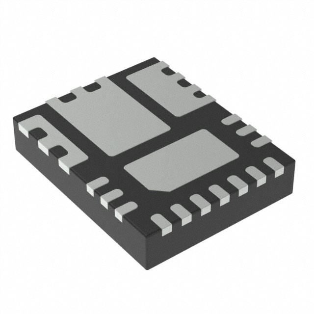
• Very Small, Low Profile 4mm x 5mm QFN Package
• 12V and 24V Distributed Power Systems
• General Purpose POL DC‐DC Converters
• Game Consoles and Graphics Cards
BASIC APPLICATION
EFFICIENCY
95%
90%
85%
Efficiency
80%
75%
70%
65%
60%
VIN = 19V
VIN = 12V
VIN = 8V
55%
50%
45%
0.01
Figure 1: IR3475 Basic Application Circuit
1
March 27, 2013 | V2.2 | PD97602
0.1
1
Load Current (A)
Figure 2: IR3475 Efficiency
10
�10A Highly Integrated SupIRBuckTM
IR3475
ORDERING INFORMATION
IR3475 ―
Package
M
Tape & Reel Qty
750
Part Number
IR3475MTR1PBF
M
4000
IR3475MTRPBF
PBF – Lead Free
TR – Tape and Reel
M – Package Type
MARKING INFORMATION
Site/Date/Marking Code
Lot Code
3475
?YWW?
xxxxx
Pin 1 Identifier
PIN DIAGRAM
θ JA = 32o C / W
θ J - PCB = 2o C / W
2
March 27, 2013 | V2.2 | PD97602
�10A Highly Integrated SupIRBuckTM
IR3475
FUNCTIONAL BLOCK DIAGRAM
Figure 3: IR3475 Functional Block Diagram
3
March 27, 2013 | V2.2 | PD97602
�IR3475
10A Highly Integrated SupIRBuckTM
TYPICAL APPLICATION
+3.3V
VCC
TP1
VINS
R1
10K
VIN
R2
10K
TP2
VIN
C1
1uF
EN
TP4
EN
C2
22uF
+ C3
68uF
4
3
FCCM
R3
200K
TP5
PGND
C4
0.22uF
R4
13.7K
14
13
VIN
BOOT
FF
FB
C10
47uF
C11
open
C12
0.1uF
TP10
PGND
C24
open
TP24
PGNDS
SS
NC1
8
TP14
+3.3V
C9
330uF
C15
open
C16
open
C17
open
C18
open
C19
open
C26
open
C27
open
PGND
7
C20
0.1uF
C8
open
R13
open
12
PHASE
C7
open
11
6
SS
IR3475
GND1
TP7
VOUT
C13
open
C6
open
PGOOD
VCC
5
FB
TP13
SS
VOUT
R6
open
ISET
NC2
4
VSW
U1
IR3475
FCCM
10
3
PGOOD
EN
GND
2
3VCBP
1
R5
10K
15
16
L1
1.5uH
+3.3V
TP11
PGOOD
TP23
VOUTS
TP6
PGNDS
ISET
17
VSW
9
1
2
SW1
EN / FCCM
+3.3V
9
10
+Vout2s -Vout2s
5
8
-Vdd2s
+Vout1s -Vout1s
4
3
C22
open
-Vdd1s
Q1
open
1
TP28
VID
+Vdd2s
R8
2.55K
2
R10
open
TP18
VOLTAGE SENSE
VOUT
R9
open
3
R11
20
+3.3V
TP25
B
2
TP27
A
1
C23
open
+Vins
VCC
+Vdd1s
6
R7
2.80K
-Vins
C14
open
VCC
TP17
PGND
C25
1uF
VIN
TP16
VCC
R12
4.99 ohms
7
C21
1uF
TP26
AGND
Figure 4: Demoboard Schematic for VOUT = 1.05V, FS = 300kHz
DEMOBOARD BILL OF MATERIALS
QTY
REFERENCE DESIGNATOR
VALUE
DESCRIPTION
MANUFACTURER
PART NUMBER
3
1
2
1
1
1
1
1
3
1
1
1
1
1
1
1
1
C1, C21, C25
C10
C12, C20
C2
C3
C4
C9
L1
R1, R2, R5
R11
R12
R3
R4
R7
R8
SW1
U1
1.00uF
47uF
0.100uF
22.0uF
68uF
0.22uF
330uF
1.5uH
10.0K
20
4.99
200K
13.7K
2.80K
2.55K
SPST
IR3475
capacitor, X7R, 1.00uF, 25V, 0.1, 0603
capacitor, 47uF, 6.3V, 805
capacitor, X7R, 0.100uF, 25V, 0.1, 603
capacitor, X5R, 22.0uF, 16V, 20%, 1206
capacitor, electrolytic, 68uF, 25V, 0.2, SMD
capacitor, X5R, 0.22uF, 10V, 0.1, 0603
capacitor, electrolytic, 330uF, 2.5V, 0.2, 7343
inductor, ferrite, 1.5uH, 16.0A, 3.8mOhm, SMT
resistor, thick film, 10.0K, 1/10W, 0.01, 0603
resistor, thick film, 20, 1/10W, 0.01, 603
resistor, thick film, 4.99, 1/10W, 0.01, 603
resistor, thick film, 200K, 1/10W, 0.01, 603
resistor, thick film, 13.7K, 1/10W, 0.01, 603
resistor, thick film, 2.80K, 1/10W, 0.01, 603
resistor, thick film, 2.55K, 1/10W, 0.01, 0603
switch, DIP, SPST, 2 position, SMT
4mm x 5mm QFN
Murata
TDK
TDK
Taiyo Yuden
Panasonic
TDK
Sanyo
Cyntec
KOA
KOA
Vishay/Dale
KOA
KOA
KOA
KOA
C&K Components
IRF
GRM188R71E105KA12D
C2012X5R0J476M
C1608X7R1E104K
EMK316BJ226ML‐T
EEV‐FK1E680P
C1608X5R1A224K
2R5TPE330M9
PIMB104T‐1R5MS‐39
RK73H1J1002F
RK73H1JLTD20R0F
CRCW06034R99FNEA
RK73H1JLTD2003F
RK73H1JLTD1372F
RK73H1JLTD2801F
RK73H1J2551F
SD02H0SK
IR3475MTRPBF
4
March 27, 2013 | V2.2 | PD97602
�10A Highly Integrated SupIRBuckTM
IR3475
PIN DESCRIPTIONS
PIN #
PIN NAME
I/O LEVEL
PIN DESCRIPTION
1
FCCM
3.3V
Forced Continuous Conduction Mode (CCM). Ground this pin to enable diode
emulation mode or discontinuous conduction mode (DCM). Pull this pin to 3.3V
to operate in CCM under all load conditions.
2
ISET
3
PGOOD
5V
4, 17
GND
Reference
5
FB
3.3V
Inverting input to PWM comparator, OVP / PGOOD sense.
6
SS
3.3V
Soft start/shutdown. This pin provides user programmable soft‐start function.
Connect an external capacitor from this pin to GND to set the startup time of the
output voltage. The converter can be shutdown by pulling this pin below 0.3V.
7
NC
‐
Connecting resistor to PHASE pin sets over current trip point.
Power good open drain output – pull up with a resistor to 3.3V
Bias return and signal reference.
‐
For internal LDO. Bypass with a 1.0µF capacitor to AGND. A resistor in series with
the bypass capacitor may be required in single‐ground plane designs. Refer to
Layout Recommendation for details.
8
3VCBP
3.3V
9
NC
‐
10
VCC
5V
11
PGND
Reference
12
PHASE
VIN
Phase node (or switching node) of MOSFET half bridge.
13
VIN
VIN
Input voltage for the system.
14
BOOT
VIN + VCC
Bootstrapped gate drive supply – connect a capacitor to PHASE.
15
FF
VIN
Input voltage feed forward – sets on‐time with a resistor to VIN.
16
EN
5V
Enable pin to turn on and off the device. Use two external resistors to set the
turn on threshold (see Electrical Specifications) for input voltage monitoring.
‐
VCC input. Gate drive supply. A minimum of 1.0µF ceramic capacitor is required.
Power return.
5
March 27, 2013 | V2.2 | PD97602
�10A Highly Integrated SupIRBuckTM
IR3475
ABSOLUTE MAXIMUM RATINGS
Stresses beyond those listed under “Absolute Maximum Ratings” may cause permanent damage to the device. These are
stress ratings only and functional operation of the device at these or any other conditions beyond those indicated in the
operational sections of the specifications are not implied.
VIN, FF
‐0.3V to 30V
VCC, PGOOD, EN
‐0.3V to 8V
BOOT
‐0.3V to 38V
PHASE
‐0.3V to 30V (DC), ‐5V (100ns)
BOOT to PHASE
‐0.3V to 8V
ISET
‐0.3V to 30V, 30mA
PGND to GND
‐0.3V to +0.3V
All other pins
‐0.3V to 3.9V
Storage Temperature Range
‐65°C to 150°C
Junction Temperature Range
‐40°C to 150°C
ESD Classification
JEDEC Class 1C
Moisture Sensitivity Level
JEDEC Level 2 @ 260°C (Note 2)
6
March 27, 2013 | V2.2 | PD97602
�IR3475
10A Highly Integrated SupIRBuckTM
ELECTRICAL SPECIFICATIONS
RECOMMENDED OPERATING CONDITIONS FOR RELIABLE OPERATION WITH MARGIN
UNITS
SYMBOL
MIN
MAX
Recommended VIN Range
VIN
3
27*
Recommended VCC Range
VCC
4.5
5.5
Recommended Output Voltage Range
VOUT
0.5
12
Recommended Output Current Range
IOUT
0
10
A
Recommended Switching Frequency
F S
N/A
750
kHz
Recommended Operating Junction Temperature
TJ
‐40
125
°C
V
* PHASE pin must not exceed 30V.
ELECTRICAL CHARACTERISTICS
Unless otherwise specified, these specifications apply over VIN = 12V, 4.5V 0.5. Increasing ESR is the most effective way to stabilize
the system, but the tradeoff is the larger output voltage
ripple.
System with all ceramic output capacitors:
For applications with all ceramic output capacitors, the ESR
is usually too small to meet the stability criteria. In these
applications, external slope compensation is necessary to
make the loop stable. The ramp injection circuit, composed
of R6, C13, and C14, shown in Figure 4 is required.
The inductor current ripple sensed by R6 and C13 is AC
coupled to the FB pin through C14. C14 is usually chosen
between 1 to 10nF, and C13 between 10 to 100nF. R6
should then be chosen such that L/DCR = C13*R6.
Boot Circuit:
Q1
Q2
Figure 30: Current Path of Power Stage
17
March 27, 2013 | V2.2 | PD97602
�10A Highly Integrated SupIRBuckTM
IR3475
PCB METAL AND COMPONENT PLACEMENT
• Pad lands (the 4 big pads) length and width
should be equal to maximum part pad length and
width. However, the minimum metal to metal
spacing should be no less than; 0.17mm for 2 oz.
Copper or no less than 0.1mm for 1 oz. Copper or
no less than 0.23mm for 3 oz. Copper.
• Lead lands (the 13 IC pins) width should be equal
to nominal part lead width. The minimum lead to
lead spacing should be ≥ 0.2mm to minimize
shorting.
• Lead land length should be equal to maximum
part lead length + 0.3 mm outboard extension.
The outboard extension ensures a large toe fillet
that can be easily inspected.
Figure 31: Metal and Component Placement
18
March 27, 2013 | V2.2 | PD97602
�10A Highly Integrated SupIRBuckTM
* Contact International Rectifier to receive an electronic PCB Library file in your preferred format
19
March 27, 2013 | V2.2 | PD97602
IR3475
�10A Highly Integrated SupIRBuckTM
IR3475
SOLDER RESIST
• It is recommended that the lead lands are Non
Solder Mask Defined (NSMD). The solder resist
should be pulled away from the metal lead lands
by a minimum of 0.025mm to ensure NSMD
pads.
• Ensure that the solder resist in between the lead
lands and the pad land is ≥ 0.15mm due to the
high aspect ratio of the solder resist strip
separating the lead lands from the pad land.
• The land pad should be Solder Mask Defined
(SMD), with a minimum overlap of the solder
resist onto the copper of 0.05mm to
accommodate solder resist misalignment.
Figure 32: Solder Resist
* Contact International Rectifier to receive an electronic PCB Library file in your preferred format
20
March 27, 2013 | V2.2 | PD97602
�10A Highly Integrated SupIRBuckTM
IR3475
STENCIL DESIGN
• The Stencil apertures for the lead lands should be
approximately 80% of the area of the lead lads.
Reducing the amount of solder deposited will
minimize the occurrences of lead shorts. If too
much solder is deposited on the center pad the
part will float and the lead lands will open.
• The maximum length and width of the land pad
stencil aperture should be equal to the solder
resist opening minus an annular 0.2mm pull back
in order to decrease the risk of shorting the
center land to the lead lands when the part is
pushed into the solder paste.
Figure 33: Stencil Design
* Contact International Rectifier to receive an electronic PCB Library file in your preferred format
21
March 27, 2013 | V2.2 | PD97602
�10A Highly Integrated SupIRBuckTM
IR3475
PACKAGE INFORMATION
Figure 34: Package Dimensions
Data and specifications subject to change without notice.
This product has been designed and qualified for the Industrial Market (Note2).
Qualification Standards can be found on IR’s Web site.
IR WORLD HEADQUARTERS: 233 Kansas St., El Segundo, California 90245, USA Tel: (310) 252-7105
TAC Fax: (310) 252-7903
Visit us at www.irf.com for sales contact information.
www.irf.com
22
March 27, 2013 | V2.2 | PD97602
�