PD-60329
IR3820MPbF
SupIRBuck
TM
HIGHLY INTEGRATED 12A
WIDE-INPUT VOLTAGE, SYNCHRONOUS BUCK REGULATOR
Features
•
•
•
•
•
•
•
•
•
•
•
•
•
•
Wide Input Voltage Range 2.5V to 21V
Wide Output Voltage Range 0.6V to 12V
Continuous 12A Load Capability
600kHz High Frequency Operation
Programmable Over-Current Protection
Programmable PGood Output
Hiccup Current Limit
Precision Reference Voltage (0.6V)
Programmable Soft-Start
Pre-Bias Start-up
Thermal Protection
Thermally Enhanced Package
Small Size 5mmx6mm QFN
Pb-Free (RoHS Compliant)
Applications
•
•
•
•
•
•
•
•
Distributed Point-of-Loads
Server and Workstations
Embedded Systems
Storage Systems
DDR Applications
Graphics Cards
Game Consoles
Computing Peripheral Voltage Regulators
Description
The IR3820 SupIRBuckTM is an easy-to-use, fully
integrated and highly efficient DC/DC regulator.
The onboard switching controller and MOSFETs
make the IR3820 a space-efficient solution,
providing accurate power delivery for low output
voltage applications.
The IR3820 operates from a single 4.5V to 14V
input supply and generates an output voltage
adjustable from 0.6V to 0.75*Vin at loads up to
12A.
A versatile regulator offering programmability of
startup time, power good threshold and current
limit, the IR3820’s fixed 600kHz switching
frequency allows the use of small external
components.
The IR3820 also features important protection
functions, such as Pre-Bias startup, hiccup
current limit and thermal shutdown to provide the
required system level security in the event of fault
conditions.
Fig. 1. Typical application diagram
11/04/08
1
�PD-60329
IR3820MPbF
ABSOLUTE MAXIMUM RATINGS
(Voltages referenced to GND)
•
VIN Supply Voltage
-0.3V to 24V
•
Vcc Supply Voltage
-0.3V to 16V
•
Vc Supply Voltage
-0.3V to 30V
•
SW
-0.3V to 30V
•
PGood
-0.3V to 16V
•
Fb,COMP,SS,Vsns
-0.3V to 3.5V
•
OCSet
10mA
•
AGnd to PGnd
-0.3V to +0.3V
•
Storage Temperature Range
-65°C To 150°C
•
Operating Junction Temperature Range
-40°C To 150°C
•
ESD Classification
JEDEC, JESD22-A114
•
Moisture Sensitivity Level
JEDEC Level 3 @ 260oC
Caution: Stresses beyond those listed under “Absolute Maximum Rating” may cause permanent damage to the
device. These are stress ratings only and functional operation of the device at these or any other conditions beyond
those indicated in the operational sections of the specifications is not implied. Exposure to “Absolute Maximum
Rating” conditions for extended periods may affect device reliability.
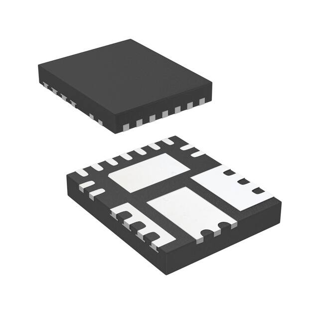
PACKAGE INFORMATION
5mm x 6mm POWER QFN
10
12
11
VIN
SW
PGnd
θJA = 35 o C / W
θJ -PCB = 2 o C / W
HG
13
VC
14
1
Vsns
15
AGnd
2
3
4
5
9
PGood
8
VCC
6
7
FB COMP AGnd AGnd SS OCSet
Fig. 2: Package outline (Top view)
ORDERING INFORMATION
11/04/08
PACKAGE
DESIGNATOR
PACKAGE
DESCRIPTION
PIN
COUNT
PARTS PER
REEL
M
IR3820MTRPbF
15
4000
M
IR3820MTR1PbF
15
750
2
�PD-60329
IR3820MPbF
Block Diagram
Fig. 3. Simplified block diagram of the IR3820.
11/04/08
3
�PD-60329
IR3820MPbF
Pin Description
Pin Name
Description
1
Vsns
PGood sense pin. Use two external resistors to program the power
good threshold.
2
Fb
3
Comp
Inverting input to the error amplifier. This pin is connected directly to the
output of the regulator via resistor divider to set the output voltage and
provide feedback to the error amplifier.
Output of error amplifier.
4
AGnd
Signal ground for internal reference and control circuitry.
5
AGnd
Signal ground for internal reference and control circuitry.
6
SS/SD
7
OCSet
Soft start / shutdown. This pin provides user programmable soft-start
function. Connect an external capacitor from this pin to signal ground
(AGnd) to set the start up time of the output voltage. The converter can
be shutdown by pulling this pin below 0.3V.
Current limit set point. A resistor from this pin to SW pin will set the
current limit threshold.
8
VCC
9
PGood
10
PGnd
11
SW
Switch node. This pin is connected to the output inductor
12
VIN
Input voltage connection pin
13
HG
14
VC
15
AGnd
This pin is connected to the high side Mosfet gate. Connect a small
capacitor from this pin to switch node (SW).
This pin powers the high side driver and must be connected to a voltage
higher than input voltage. A minimum of 0.1uF high frequency capacitor
must be connected from this pin to the power ground (PGnd).
Signal ground for internal reference and control circuitry.
This pin provides biasing voltage for the internal blocks of the IC. It also
powers the low side driver. A minimum of 0.1uF, high frequency
capacitor must be connected from this pin to power ground (PGnd).
Power Good status pin. Output is open collector. Connect a pull up
resistor from this pin to Vcc.
Power Ground. This pin serves as a separated ground for the MOSFET
drivers and should be connected to the system’s power ground plane.
Pins 4, 5 and 15 need to be connected together on system board.
11/04/08
4
�PD-60329
IR3820MPbF
Recommended Operating Conditions
Symbol
Vin
Vcc
Vc
Vo
Io Note1
Tj
Definition
Input Voltage
Supply Voltage
Supply Voltage
Output Voltage
Output Current
Junction Temperature
Min
Max
2.5
4.5
Vin + 5V
0.6
0
-40
21
14
28
12
12
125
Units
V
A
C
o
Electrical Specifications
Unless otherwise specified, these specification apply over Vin=Vcc=Vc=12V, 0oC
很抱歉,暂时无法提供与“IR3820MTRPBF”相匹配的价格&库存,您可以联系我们找货
免费人工找货