DCDC Converter
25A Highly Integrated SupIRBuck®
Single-Input Voltage, Synchronous
Buck Regulator
SupIRBuck
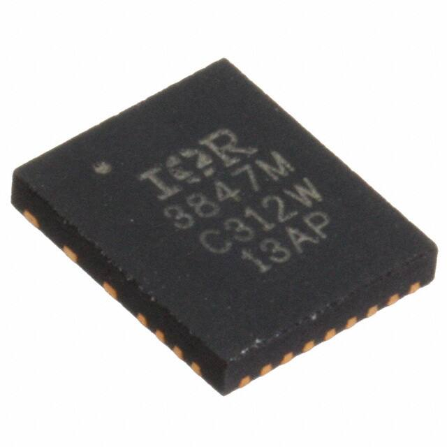
IR3847
DESCRIPTION
FEATURES
Single 5V to 21V application
Wide Input Voltage Range from 1.5V to 21V with
external Vcc
Output Voltage Range: 0.6V to 0.86*PVin
0.5% accurate Reference Voltage
Enhanced line/load regulation with Feed-Forward
Programmable Switching Frequency up to
1.5MHz
Internal Digital Soft-Start
Enable input with Voltage Monitoring Capability
Remote Sense Amplifier with True Differential
Voltage Sensing
Thermally compensated current limit and Hiccup
Mode Over Current Protection
Smart LDO to enhance efficiency
Vp for tracking applications and sequencing
Vref is available externally to enable margining
External synchronization with Smooth Clocking
Dedicated output voltage sensing for power good
indication and overvoltage protection which
remains active even when Enable is low.
Enhanced Pre-Bias Start up
Body Braking to improve transient
Integrated MOSFET drivers and Bootstrap diode
Thermal Shut Down
Post Package trimmed rising edge dead-time
Programmable Power Good Output with tracking
Small Size 5mm x 6mm PQFN
o
o
Operating Junction Temp: -40 C 1.0V
EN
> 1.2V
input. In this operating mode Vref is left floating.
Figure 6 shows the recommended startup sequence
for sequenced operation of IR3847 with Enable used
as logic input. Figure 7 shows the recommended
startup sequence for tracking operation of IR3847 with
Enable used as logic input. For this mode of
operation, Vref should be connected to LGND.
PRE-BIAS STARTUP
Intl_SS
IR3847 is able to start up into pre-charged output,
which prevents oscillation and disturbances of the
output voltage.
Vo
Figure 5: Recommended startup for Normal operation
PVin=Vin
Vcc
Vp
> 1.2V
EN
Intl_SS
The output starts in asynchronous fashion and keeps
the synchronous MOSFET (Sync FET) off until the
first gate signal for control MOSFET (Ctrl FET) is
generated. Figure 8 shows a typical Pre-Bias condition
at start up. The sync FET always starts with a narrow
pulse width (12.5% of a switching period) and
gradually increases its duty cycle with a step of 12.5%
until it reaches the steady state value. The number of
these startup pulses for each step is 16 and it’s
internally programmed. Figure 9 shows the series of
16x8 startup pulses.
Vo
[V]
Vo
Figure 6: Recommended startup for sequencing
operation (ratiometric or simultaneous)
Pre-Bias
Voltage
PVin=Vin
[Time]
Vcc
Figure 8: Pre-Bias startup
VDDQ
Vp
EN
VDDQ/2
...
HDRv
12.5%
> 1.2V
...
LDRv
Vref
...
...
25%
...
...
87.5%
...
...
...
0V
16
16
End of
PB
...
Vo
VTT Tracking
Figure 7: Recommended startup for memory tracking
operation (Vtt-DDR)
Figure 5 shows the recommended startup sequence
for the normal (non-tracking, non-sequencing)
operation of IR3847, when Enable is used as a logic
21
Rev 3.7
Figure 9: Pre-Bias startup pulses
SOFT-START
IR3847 has an internal digital soft-start to control the
output voltage rise and to limit the current surge at the
start-up. To ensure correct start-up, the soft-start
sequence initiates when the Enable and VCC rise
May 17, 2016
�IR3847
above their UVLO thresholds and generate the Power
On Ready (POR) signal. The internal soft-start
(Intl_SS) signal linearly rises with the rate of 0.4mV/µs
from 0V to 1.5V. Figure 10 shows the waveforms
during soft start. The normal Vout startup time is fixed,
and is equal to:
Tstart
0.75V 0.15V 1.5mS
0.4mV / S
Table 1: Switching Frequency(Fs) vs. External
Resistor(Rt)
Rt (KΩ)
80.6
60.4
48.7
39.2
34
29.4
26.1
23.2
21
19.1
17.4
16.2
15
(1)
During the soft start the over-current protection (OCP)
and over-voltage protection (OVP) is enabled to
protect the device for any short circuit or over voltage
condition.
POR
3.0V
Freq
(KHz)
300
400
500
600
700
800
900
1000
1100
1200
1300
1400
1500
1.5V
0.75V
SHUTDOWN
Intl_SS
0.15V
IR3847 can be shutdown by pulling the Enable pin
below its 1.0V threshold. During shutdown the high
side and the low side drivers are turned off.
Vout
t1 t2
t3
Figure 10: Theoretical operation waveforms during
soft-start (non tracking / non sequencing)
OPERATING FREQUENCY
The switching frequency can be programmed between
300kHz – 1500kHz by connecting an external resistor
from Rt pin to LGnd. Table 1 tabulates the oscillator
frequency versus Rt.
OVER CURRENT PROTECTION
The Over Current (OC) protection is performed by
sensing the inductor current through the RDS(on) of the
Synchronous MOSFET. This method enhances the
converter’s efficiency, reduces cost by eliminating a
current sense resistor and any layout related noise
issues. The Over Current (OC) limit can be set to one
of three possible settings by floating the OCset pin, by
pulling up the OCset pin to VCC, or pulling down the
OCset pin to PGnd. The current limit scheme in the
IR3847 uses an internal temperature compensated
current source to achieve an almost constant OC limit
over temperature.
Over Current Protection circuit senses the inductor
current flowing through the Synchronous MOSFET.
To help minimize false tripping due to noise and
transients, inductor current is sampled for about 30 nS
on the downward inductor current slope approximately
12.5% of the switching period before the inductor
current valley. However, if the Synchronous MOSFET
is on for less than 12.5% of the switching period, the
current is sampled approximately 40nS after the start
of the downward slope of the inductor current. When
22
Rev 3.7
May 17, 2016
�IR3847
the sampled current is higher than the OC Limit, an
OC event is detected.
When an Over Current event is detected, the
converter enters hiccup mode. Hiccup mode is
performed by latching the OC signal and pulling the
Intl_SS signal to ground for 20.48 mS (typ.). OC
signal clears after the completion of hiccup mode and
the converter attempts to return to the nominal output
voltage using a soft start sequence. The converter will
repeat hiccup mode and attempt to recover until the
overload or short circuit condition is removed.
Because the IR3847 uses valley current sensing, the
actual DC output current limit will be greater than OC
limit. The DC output current is approximately half of
peak to peak inductor ripple current above selected
OC limit. OC Limit, inductor value, input voltage,
output voltage and switching frequency are used to
calculate the DC output current limit for the converter.
Equation (2) to determine the approximate DC output
current limit.
I OCP I LIMIT
IOCP
ILIMIT
Δi
i
2
(2)
= DC current limit hiccup point
= Current Limit Valley Point
= Inductor ripple current
Current Limit
Hiccup
Tblk_Hiccup
20.48 mS*
IL
0
HDrv
...
0
LDrv
...
0
PGD
*typical filter delay
0
Automatic restart is initiated when the sensed
temperature drops within the operating range. There
o
is a 20 C hysteresis in the thermal shutdown
threshold.
REMOTE VOLTAGE SENSING
True differential remote sensing in the feedback loop
is critical to high current applications where the output
voltage across the load may differ from the output
voltage measured locally across an output capacitor
at the output inductor, and to applications that require
die voltage sensing.
The RS+ and RS- pins of the IR3847 form the inputs
to a remote sense differential amplifier (RSA) with
high speed, low input offset and low input bias current
which ensure accurate voltage sensing and fast
transient response in such applications.
The input range for the differential amplifier is limited
to 1.5V below the VCC rail. Note that IR3847
incorporates a smart LDO which switches the VCC rail
voltage depending on the loading. When determining
the input range assume the part is in light load and
using the lower VCC rail voltage.
There are two remote sense configurations that are
usually implemented. Figure 12 shows a general
remote sense (RS) configuration. This configuration
allows the RSA to monitor output voltages above
VCC. A resistor divider is placed in between the
output and the RSA to provide a lower input voltage to
the RSA inputs. Typically, the resistor divider is
calculated to provide VREF (0.6V) across the RSA
inputs which is then outputted to RSo. The input
impedance of the RSA is 63 KOhms typically and
should be accounted for when determining values for
the resistor divider. To account for the input
impedance, assume a 63 KOhm resistor in parallel to
the lower resistor in the divider network.
The
compensation is then designed for 0.6V to match the
RSo value.
Figure 11: Timing Diagram for Current Limit Hiccup
THERMAL SHUTDOWN
Temperature sensing is provided inside IR3847. The
o
trip threshold is typically 145 C. When trip threshold is
exceeded, thermal shutdown turns off both MOSFETs
and resets the internal soft start.
23
Rev 3.7
Low voltage applications can use the second remote
sense configuration. When the output voltage range
is within the RSA input specifications, no resistor
divider is needed in between the converter output and
RSA. The second configuration is shown in Figure
13. The RSA is used as a unity gain buffer and
compensation is determined normally.
May 17, 2016
�IR3847
Vout
(< VCC-1.5V)
-
RSo
Compensation
Resistor Divider
RS+
+
RSA
RS-
+
FB
-
+
Vout
(< VCC-1.5V)
-
RS+
RSo
Vo
RSA
RS-
Compensation
Figure 12: General Remote Sense Configuration
+
IR3847 incorporates an internal phase lock loop (PLL)
circuit which enables synchronization of the internal
oscillator to an external clock. This function is
important to avoid sub-harmonic oscillations due to
beat frequency for embedded systems when multiple
point-of-load (POL) regulators are used. A multifunction pin, Rt/Sync, is used to connect the external
clock. If the external clock is present before the
converter turns on, Rt/Sync pin can be connected to
the external clock signal solely and no other resistor is
needed. If the external clock is applied after the
converter turns on, or the converter switching
frequency needs to toggle between the external clock
frequency and the internal free-running frequency, an
external resistor from Rt/Sync pin to LGnd is required
to set the free-running frequency.
When an external clock is applied to Rt/Sync pin after
the converter runs in steady state with its free-running
frequency, a transition from the free-running
frequency to the external clock frequency will happen.
This transition is to gradually make the actual
switching frequency equal to the external clock
frequency, no matter which one is higher. When the
external clock signal is removed from Rt/Sync pin, the
switching frequency is also changed to free-running
Synchronize to the
external clock
Free Running
Frequency
-
EXTERNAL SYNCHRONIZATION
Rev 3.7
An internal circuit is used to change the PWM ramp
slope according to the clock frequency applied on
Rt/Sync pin. Even though the frequency of the
external synchronization clock can vary in a wide
range, the PLL circuit keeps the ramp amplitude
constant, requiring no adjustment of the loop
compensation. PVin variation also affects the ramp
amplitude, which will be discussed separately in FeedForward section.
FB
Figure 13: Remote Sense Configuration for Vout less
than VCC-1.5V
24
gradually. In order to minimize the impact from these
transitions to output voltage, a diode is recommended
to add between the external clock and Rt/Sync pin.
Figure 14 shows the timing diagram of these
transitions.
Return to freerunning freq
...
SW
Gradually change
Gradually change
...
Fs1
SYNC
Fs1
Fs2
Figure 14: Timing Diagram for Synchronization
to the external clock (Fs1>Fs2 or Fs1
很抱歉,暂时无法提供与“IR3847MTRPBF”相匹配的价格&库存,您可以联系我们找货
免费人工找货- 国内价格
- 1+52.36920
- 10+51.13800
- 30+50.31720