IR3888
IR3888 OptiMOS™ IPOL
25 A single-voltage synchronous Buck regulator
Features
Single 4.3 V to 17 V application or Wide Input Voltage Range from 2.0 V to 17 V with an External VCC
Precision Reference Voltage (0.6 V +/- 0.5%)
Enhanced Fast COT engine stable with Ceramic Output Capacitors and No External Compensation
Optional Forced Continuous Conduction Mode and Diode Emulation for Enhanced Light Load Efficiency
Programmable Switching Frequency from 600 kHz to 2 MHz
Monotonic Start-Up with Four Selectable Soft-Start Time & Enhanced Pre-Bias Start-Up
Thermally Compensated Internal Over Current Protection with Four Selectable Settings
Enable input with Voltage Monitoring Capability & Power Good Output
Thermal Shut Down
Operating Temp: -40 °C < Tj < 125 °C
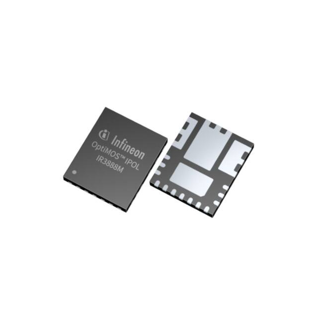
Small Size: 6 mm x 5 mm PQFN
Halogen-free and RoHS2 Compliant with Exemption 7a
Potential applications
Server Applications
Storage Applications
Telecom & Datacom Applications
Distributed Point of Load Power Architectures
Product validation
Qualified for industrial applications according to the relevant tests of JEDEC47/20/22
Description
The IR3888 is an easy-to-use, fully integrated dc - dc Buck regulator. The onboard PWM controller and OptiMOS™
FETs with integrated bootstrap diode make IR3888 a small footprint solution, providing high-efficient power
delivery. Furthermore, it uses a fast Constant On-Time (COT) control scheme, which simplifies the design efforts
and achieves fast control response.
The IR3888 has an internal low dropout voltage regulator, allowing operations with a single supply. It can also
operate with an external bias supply, extending the operating input voltage (PVin) range.
The IR3888 is a versatile regulator, offering programmable switching frequency from 600 kHz to 2 MHz, four
selectable current limits, four selectable soft-start time, Forced Continuous Conduction Mode (FCCM) and Diode
Emulation Mode (DEM) operation.
It also features important protection functions, such as pre-bias start-up, thermally compensated current limits,
over voltage and under voltage protection, and thermal shutdown to give required system level security in the
event of fault conditions.
Final Datasheet
www.infineon.com
Please read the Important Notice and Warnings at the end of this document
page 1 of 49
V2.3
2021-7-20
�IR 888 OptiMOS™ IPOL
25 A single-voltage synchronous Buck regulator
Table of contents
Table of contents
Features ........................................................................................................................................ 1
Potential applications ..................................................................................................................... 1
Product validation .......................................................................................................................... 1
Description .................................................................................................................................... 1
Table of contents ............................................................................................................................ 2
1
Ordering information ............................................................................................................. 4
2
Functional block diagram........................................................................................................ 5
3
Typical application diagram .................................................................................................... 6
4
Pin descriptions ..................................................................................................................... 7
5
Absolute maximum ratings ..................................................................................................... 9
6
6.1
Thermal Characteristics ......................................................................................................... 10
Thermal Characteristics ........................................................................................................................ 10
7
7.1
7.2
Electrical specifications ......................................................................................................... 11
Recommended operating conditions................................................................................................... 11
Electrical characteristics ....................................................................................................................... 12
8
8.1
8.2
8.3
8.4
Typical efficiency and power loss curves.................................................................................. 15
PVin = Vin = 12 V, Fsw = 600 kHz ................................................................................................................ 15
PVin = Vin = 12 V, Fsw = 800 kHz ................................................................................................................ 16
PVin = Vin = 12 V, Fsw = 1000 kHz............................................................................................................... 17
PVin = Vin = VCC = 5 V, Fsw = 600 kHz ........................................................................................................ 18
9
Thermal De-rating curves ....................................................................................................... 19
10
RDS(ON) of MOSFET Over Temperature ........................................................................................ 20
11
Typical operating characteristics (-40 °C ≤ Tj ≤ +125 °C) .............................................................. 21
12
Theory of operation ............................................................................................................... 24
12.1
Fast Constant On-Time Control ............................................................................................................ 24
12.2
Enable .................................................................................................................................................... 24
12.3
FCCM and DEM Operation ..................................................................................................................... 25
12.4
Pseudo Constant Switching Frequency................................................................................................ 25
12.5
Soft-start ................................................................................................................................................ 26
12.6
Pre-bias Start-up ................................................................................................................................... 27
12.7
Internal Low – Dropout (LDO) Regulator .............................................................................................. 27
12.8
Over Current Protection (OCP) ............................................................................................................. 28
12.9
Under Voltage Protection (UVP) ........................................................................................................... 29
12.10
Over Voltage Protection (OVP) .............................................................................................................. 29
12.11
Over Temperature Protection (OTP) .................................................................................................... 30
12.12
Power Good (Pgood) Output ................................................................................................................ 30
12.13
Minimum On – Time and Minimum Off – Time ..................................................................................... 31
12.14
Selection of Feedforward Capacitor and Feedback Resistors ............................................................. 31
12.15
Resistors for Configuration Pins ........................................................................................................... 32
13
Design example..................................................................................................................... 33
13.1
Enabling the IR3888............................................................................................................................... 33
13.2
Programming the Switching Frequency and Operation Mode ............................................................ 33
13.3
Selecting Input Capacitors .................................................................................................................... 33
13.4
Inductor Selection ................................................................................................................................. 34
Final Datasheet
2 of 49
V2.3
2021-7-20
�IR 888 OptiMOS™ IPOL
25 A single-voltage synchronous Buck regulator
Table of contents
13.5
13.6
13.7
13.8
13.9
Output Capacitor Selection .................................................................................................................. 34
Output Voltage Programming............................................................................................................... 35
Feedforward Capacitor ......................................................................................................................... 35
Bootstrap Capacitor .............................................................................................................................. 35
VIN and VCC/LDO bypass Capacitor ..................................................................................................... 35
14
Application Information ......................................................................................................... 36
14.1
Application Diagram.............................................................................................................................. 36
14.2
Typical Operating Waveforms............................................................................................................... 36
15
Layout Recommendations...................................................................................................... 39
15.1
Solder Mask ........................................................................................................................................... 43
15.2
Stencil Design ........................................................................................................................................ 44
16
Package ............................................................................................................................... 45
16.1
Marking Information ............................................................................................................................. 45
16.2
Dimensions ............................................................................................................................................ 45
16.3
Tape and Reel Information ................................................................................................................... 46
17
Environmental Qualifications ................................................................................................. 47
18
Evaluation Boards and Support Documentation ....................................................................... 48
Revision history............................................................................................................................. 49
Final Datasheet
3 of 49
V2.3
2021-7-20
�IR 888 OptiMOS™ IPOL
25 A single-voltage synchronous Buck regulator
Ordering information
1
Ordering information
1.
Ordering Information
Sales Product Name
Package Type
IR3888MTRPBF
QFN 6 mm x 5 mm
Standard Pack Form and Qty
Tape and Reel
Orderable Part Number
5000
IR3888MTRPBFAUMA1
IR3888MTRPBF
A1
UM
A
FB
1
SS/ Latch
2
VSENM
3
NC
EN
22
21
BOOT
20
Designator
Packing type
Tape & Reel
Moisture
protection packing
Dry
Packing size
330 mm
Halogen Free
RoHS compliant
Total lead free
Yes
Yes
No
PVIN
PVIN
PVIN
19
18
17
16
SW
15
SW
14
SW
AGND
AGND
4
23
Ton/ Mode
5
ILIM
6
PGOOD
7
8
VSNS
9
10
VIN VCC/ LDO
11
12
PGND
PGND
13
PGND
Figure 1 Package Top View
Final Datasheet
4 of 49
V2.3
2021-7-20
�IR 888 OptiMOS™ IPOL
25 A single-voltage synchronous Buck regulator
Functional block diagram
Functional block diagram
2
AGND
PGood
VCC/LDO
Vin
AGND
VREF
*70%
POR
UVP OTP
+
-
LDO
EN
Fault
VCC
AGND
VREF
*120%
LDrVin
BOOT
OVP
+
-
Hysteresis
=5%
Turn-on Delay
PVIN
VSNS
PGood
+
VREF
*90%
Q
S
Prebias
Q
R
Fault
HDrVin
HDrv
Hysteresis
=5%
-
POR
VCC
4.0V
+
POR
-
GATE
DRIVE
LOGIC
Hiccup
OVP
SW
VCC
OTP
EN
+
1.2V
Fault
-
LDrv
LDrVin
PWM
SOFT
START
SS/Latch
PWM
COMP
SS
+
+-
ADAPTIVE
ON-TIME
GENERATOR
SET
FB
ZC
Zero Cross
DETECTION
PGND
PGND
SW
OCP
Floor
GENERATOR
+
OVP
Latch Off
-
+
+
VSENM
RAMP
GENERATOR
Hiccup
UVP
S
Q
R
TON/
MODE
ILIM
-
VREF
SW
ILIM Ref
20ms
Delay
Figure 2 Block diagram
Final Datasheet
5 of 49
V2.3
2021-7-20
�IR 888 OptiMOS™ IPOL
25 A single-voltage synchronous Buck regulator
Typical application diagram
Typical application diagram
3
4.3V VPG(upper)
1
2
PG = 3.3 V
Max
Unit
mA
0.5
V
ms
3.5
1
µs
µA
Thermal Shutdown
Thermal Shutdown
Note 11
140
Hysteresis
Note 11
20
°C
Note:
11. Guaranteed by construction and not tested in production
12. Cold temperature performance is guaranteed via correlation using statistical quality control. Not tested in
production.
13. The Ton is trimmed so that the target switching frequency is achieved at around 10A load current using
EVAL_3888_1Vout demo board.
Final Datasheet
14 of 49
V2.3
2021-7-20
�IR 888 OptiMOS™ IPOL
25 A single-voltage synchronous Buck regulator
Typical efficiency and power loss curves
8
Typical efficiency and power loss curves
8.1
PVin = Vin =
V, Fsw =
kHz
PVin = Vin = 12 V, VCC = Internal LDO, Io = 0 A-25 A, Fsw = 600 kHz, Room Temperature, No Air Flow. Note that the
efficiency and power loss curves include the losses of IR3888, the inductor losses, the losses of the input and
output capacitors, and PCB trace losses. The table below shows the inductors used for each of the output
voltages in the efficiency measurement.
Table 1
Vout (V)
Inductors for PVin=Vin=12 V, Fs = 600 kHz
Lout (nH)
P/N
DCR (m)
Size (mm)
1.0
150
HCB138380D-151 (Delta)
0.15
12.4 x 8.3 x 8
1.2
220
FP1008R5-R220-R (Cooper)
0.17
10.8 x 8 x 8
1.8
220
FP1008R5-R220-R (Cooper)
0.17
10.8 x 8 x 8
2.5
350
HCBD101195-351(Delta)
0.35
10.1 x 11.4 x 9.5
3.3
350
HCBD101195-351(Delta)
0.35
10.1 x 11.4 x 9.5
5
450
HCBD101195-451(Delta)
0.35
10.1 x 11.4 x 9.5
Final Datasheet
15 of 49
V2.3
2021-7-20
�IR 888 OptiMOS™ IPOL
25 A single-voltage synchronous Buck regulator
Typical efficiency and power loss curves
8.2
PVin = Vin =
V, Fsw = 8
kHz
PVin = Vin = 12 V, VCC = Internal LDO, Io = 0 A-25 A, Fsw = 800 kHz, Room Temperature, No Air Flow. Note that the
efficiency and power loss curves include the losses of IR3888, the inductor losses, the losses of the input and
output capacitors, and PCB trace losses. The table below shows the inductors used for each of the output
voltages in the efficiency measurement.
Table 2
Vout (V)
Inductors for PVin=Vin=12 V, Fsw = 800 kHz
Lout (nH)
P/N
DCR (m)
Size (mm)
1.0
150
HCB138380D-151 (Delta)
0.15
12.4 x 8.3 x 8
1.2
150
HCB138380D-151 (Delta)
0.15
12.4 x 8.3 x 8
1.8
220
FP1008R5-R220-R (Cooper)
0.17
10.8 x 8 x 8
2.5
220
FP1008R5-R220-R (Cooper)
0.17
10.8 x 8 x 8
3.3
350
HCBD101195-351(Delta)
0.35
10.1 x 11.4 x 9.5
Final Datasheet
16 of 49
V2.3
2021-7-20
�IR 888 OptiMOS™ IPOL
25 A single-voltage synchronous Buck regulator
Typical efficiency and power loss curves
8.3
PVin = Vin =
V, Fsw =
kHz
PVin = Vin = 12 V, VCC = Internal LDO, Io = 0 A-25 A, Fsw = 1000 kHz, Room Temperature, No Air Flow. Note that the
efficiency and power loss curves include the losses of IR3888, the inductor losses, the losses of the input and
output capacitors, and PCB trace losses. The table below shows the inductors used for each of the output
voltages in the efficiency measurement.
Table 3
Vout (V)
Inductors for PVin=Vin=12 V, Fsw = 1000 kHz
Lout (nH)
P/N
DCR (m)
Size (mm)
1.0
100
AH3740A-100K (ITG)
0.145
6.4 x 9.5 x 10
1.2
100
AH3740A-100K (ITG)
0.145
6.4 x 9.5 x 10
1.8
150
AH3740A-150K (ITG)
0.145
6.4 x 9.5 x 10
Final Datasheet
17 of 49
V2.3
2021-7-20
�IR 888 OptiMOS™ IPOL
25 A single-voltage synchronous Buck regulator
Typical efficiency and power loss curves
8.4
PVin = Vin = VCC = V, Fsw =
kHz
PVin = Vin = VCC = 5.0 V, Io = 0 A – 25 A, Fsw = 600 kHz, Room Temperature, No Air Flow. Note that the efficiency and
power loss curves include the losses of IR3888, the inductor losses, the losses of the input and output
capacitors and and PCB trace losses. The table below shows the inductors used for each of the output voltages
in the efficiency measurement.
Table 4
Inductors for PVin=Vin=VCC=5 V, Fsw = 600 kHz
Vout (V)
Lout (nH)
P/N
DCR (m)
Size (mm)
1.0
150
AH3740A-150K (ITG)
0.145
6.4 x 9.5 x 10
1.2
150
AH3740A-150K (ITG)
0.145
6.4 x 9.5 x 10
1.8
150
AH3740A-150K (ITG)
0.145
6.4 x 9.5 x 10
3.3
150
AH3740A-150K (ITG)
0.145
6.4 x 9.5 x 10
Final Datasheet
18 of 49
V2.3
2021-7-20
�IR 888 OptiMOS™ IPOL
25 A single-voltage synchronous Buck regulator
Thermal De-rating curves
9
Thermal De-rating curves
Measurement is done on Evaluation board of EVAL_3888. PCB is a 6-layer board with 1.5 ounce Copper for top
and bottom layer and 2 ounce Copper for the inner layers, FR4 material, size . ”x .75”.
Figure 4 Thermal de-rating curves, PVin = 12 V, Vout=1.2 V/3.3 V/5 V, fsw = 600 kHz, VCC = Internal LDO
Final Datasheet
19 of 49
V2.3
2021-7-20
�IR 888 OptiMOS™ IPOL
25 A single-voltage synchronous Buck regulator
RDS(ON) of MOSFET Over Temperature
10
RDS ON of MOSFET Over Temperature
Figure 5 RDS(on) of MOSFETs over Junction Temperature
Final Datasheet
20 of 49
V2.3
2021-7-20
�IR 888 OptiMOS™ IPOL
25 A single-voltage synchronous Buck regulator
Typical operating characteristics (-
11
C ≤ Tj ≤ +
C
Typical operating characteristics -
°C ≤ Tj ≤ +
°C
Figure 6 Typical operating characteristics (set 1 of 3)
Final Datasheet
21 of 49
V2.3
2021-7-20
�IR 888 OptiMOS™ IPOL
25 A single-voltage synchronous Buck regulator
Typical operating characteristics (-
C ≤ Tj ≤ +
C
Figure 7 Typical operating characteristics (set 2 of 3)
Final Datasheet
22 of 49
V2.3
2021-7-20
�IR 888 OptiMOS™ IPOL
25 A single-voltage synchronous Buck regulator
Typical operating characteristics (-
C ≤ Tj ≤ +
C
Figure 8 Typical operating characteristics (set 3 of 3)
Final Datasheet
23 of 49
V2.3
2021-7-20
�IR 888 OptiMOS™ IPOL
25 A single-voltage synchronous Buck regulator
Theory of operation
Theory of operation
12
Fast Constant On-Time Control
12.1
The IR3888 features a proprietary Fast Constant On-Time (COT) Control, which can provide fast load transient
response, good output regulation and minimize the design effort. Fast COT control compares the output voltage,
Vo, to a floor voltage combined with an internal ramp signal. When Vout drops below that signal, a PWM signal is
initiated to turn on the high-side FET for a fixed on-time. The floor voltage is generated from an internal
compensated error amplifier, which compares the Vout with a reference voltage. Compared to the traditional
COT control, Fast COT control significantly improves the Vout regulation.
Enable
12.2
En pin controls the on/off of the IR3888. An internal Under Voltage Lock-Out (UVLO) circuit monitors the En
voltage. When the En voltage is above an internal threshold, the internal LDO starts to ramp up. When the
VCC/LDO voltage rises above the VCC_UVLO_Start threshold, the soft-start sequence starts. The En pin can be
configured in three ways, as shown in Figure 9. With configuration 2, the Enable signal is derived from the Pvin
voltage by a set of resistive divider, REN1 and REN2. By selecting different divider ratios, users can program a
UVLO threshold voltage for the bus voltage. This is a very desirable feature because it prevents the IR3888 from
operating until Pvin is higher than a desired voltage level. For some space constrained designs, En pin can be
directly connected to Pvin without using the external resistor dividers, as shown in Configuration 3. En pin should
not be left floating. A pull down resistor in the range of tens of kilohms is recommended. Figure 10 illustrates the
corresponding start-up sequences with three En configurations.
PVin
PVin
PVin
Vin
PVin
PVin
REN1
Vin
Vcc
En
Vcc
En
IR3888
En = an external logic signal
Configuration 1
PVin
Vcc
IR3888
En
REN2
En =
��
Vin
��
+ ��
×
Configuration 2
�
IR3888
Pvin = Vin = En
Configuration 3
Figure 9 Enable Configurations
Final Datasheet
24 of 49
V2.3
2021-7-20
�IR 888 OptiMOS™ IPOL
25 A single-voltage synchronous Buck regulator
Theory of operation
Pvin= Vin=12V
PVin= Vin=En=12V
Pvin = Vin = 12V
Vcc_ UVLO
Vcc
Vcc
Vcc_UVLO
0V
0V
0V
0V
En >1.2V
Fb
Pgood Turn-on
threshold
0V
2.5ms
0V
En Threshold
0V
En = REN2/(REN1+REN2)*PVin
En Threshold
PGood
0V
En = an external logic signal
Configuration 1
Fb
Pgood Turn-on
threshold
2.5ms
0V
Pgood stays at logic low
0V
Fb
Pgood Turn-on
threshold
0V
PGood
0V
Vcc
Vcc_ UVLO
2.5ms
0V
PGood
0V
Pgood stays at logic low
Pgood stays at logic low
En =
��
��
+ ��
×
Configuration 2
�
Pvin = Vin = En
Configuration 3
Figure 10 Start-up sequence
12.3
FCCM and DEM Operation
The IR3888 offers two operation modes: Forced Continuous Conduction (FCCM) and Diode Emulation Mode
(DEM). With FCCM, the IR3888 always operates as a synchronous buck converter with a pseudo constant
switching frequency and therefore achieves small output voltage ripples. In DEM, the synchronous FET is turned
off when the inductor current is close to zero, which reduces the switching frequency and improves the efficiency
at light load. At heavy load, both FCCM and DEM operate in the same way. The operation mode can be selected
with TON/MODE pin, as shown in Table 5. It should be noted that the selection of the operation mode cannot be
changed on the fly. To load a new TON/MODE configuration, En or VCC voltage needs to be cycled.
12.4
Pseudo Constant Switching Frequency
The IR3888 offers eight programmable switching frequencies, fsw, from 600 kHz to 2 MHz, by connecting an
external resistor from TON/MODE pin to the ground. Based on the selected fsw, the IR3888 generates the
corresponding on-time of the Control FET for a given PVin and Vo, as shown by the formula below.
=
�
×
��
Where fsw is the desired switching frequency. During the operation, the IR3888 monitors PVin and Vo, and can
automatically adjust the on-time to maintain the pre-selected fsw. With the increase of the load, the switching
frequency can increase to compensate for the power losses. Therefore, the IR3888 has a pseudo constant
switching frequency.
Table 5 lists the resistors for TON/MODE pin. In this table, E96 resistors with ±1% tolerance are used. If E12
resistor values are preferred, please refer to the Section 12.15. To load a new TON/MODE configuration, En or
VCC voltage needs to be cycled.
Final Datasheet
25 of 49
V2.3
2021-7-20
�IR 888 OptiMOS™ IPOL
25 A single-voltage synchronous Buck regulator
Theory of operation
Table 5 Configuration Resistors for TON/MODE Pin
TON/MODE Resistor (kΩ
±1% Tolerance
Freq (kHz)
0
600
1.5
800
2.49
1000
3.48
1200
4.53
1400
5.76
1600
7.32
1800
8.87
2000
10.5
600
12.1
800
14
1000
16.2
1200
18.7
1400
21.5
1600
24.9
1800
28.7
2000
Ton = Floating
800
12.5
Mode
FCCM
DEM
FCCM
Soft-start
The IR3888 has an internal digital soft-start to control the output voltage rise and to limit the current surge at the
start-up. To ensure a correct start-up, the soft-start sequence initiates when the EN and VCC voltages rise above
their respective thresholds. The internal soft-start signal linearly rises from 0 V to 0.6 V in a defined time duration.
The soft-start time does not change with the output voltage. During the soft-start, the IR3888 operates in DEM
until 1ms after the output voltage ramps above the Pgood turn-on threshold. The IR3888 has four soft-start time
options selected by placing a resistor from SS/Latch pin to the ground. Table 6 lists the resistor values and its
corresponding soft-start time. In this table, E96 resistors with ±1% tolerance are used. If E12 resistor values are
preferred, please refer to the Section 12.15. For each soft-start time, there are two resistor options available.
Please note that SS/Latch pin is a multi-function pin, which is also used to select different responses for Over
Voltage Protection (OVP). To load a new SS/Latch selection, En or VCC voltage needs to be cycled.
Final Datasheet
26 of 49
V2.3
2021-7-20
�IR 888 OptiMOS™ IPOL
25 A single-voltage synchronous Buck regulator
Theory of operation
Table 6 Configuration Resistor for SS/Latch Pin
SS/Latch Resistor kΩ
±1% Tolerance
Soft-start Time
(ms)
0
1
4.53
1.5
2
5.76
Latch
2.49
4
7.32
3.48
8
8.87
10.5
1
18.7
12.1
2
21.5
No Latch
14
4
24.9
16.2
8
28.7
SS/Latch = Floating
12.6
OVP
4
Latch
Pre-bias Start-up
The IR3888 is able to start up into a pre-charged output without causing oscillations and disturbances of the
output voltage. When IR3888 starts up with a pre-biased output voltage, both control FET and Synch FET are
kept off till the internal soft-start signal exceeds the FB voltage.
12.7
Internal Low – Dropout LDO Regulator
The IR3888 has an integrated low-dropout LDO regulator, providing the bias voltage for the internal circuitry. To
minimize the standby current, the internal LDO is disabled when the En voltage is pulled low. VIN pin is the input
of the LDO. When using the internal LDO for a single rail operation, VIN pin should be connected to PVIN pin. To
save the power losses on the LDO, an external bias voltage can be used by connecting VIN pin to the VCC/LDO
pin. Figure 11 illustrates the configuration of VCC/LDO, and VIN pin.
PVin
Ext Vcc
PVin
4.7uF
PVin VIN
VCC/LDO
IR3888
PVin VIN
VCC/LDO
2.2uF ~10uF
PGND
Single rail operation with the internal LDO
IR3888
10uF
PGND
Use an external VCC
Figure 11 Configuration of Using the internal LDO or an external VCC.
Final Datasheet
27 of 49
V2.3
2021-7-20
�IR 888 OptiMOS™ IPOL
25 A single-voltage synchronous Buck regulator
Theory of operation
Section 7.1 specified the recommended operating voltage range of Vin and VCC under different configurations.
Following design guidelines are recommended when configuring the VCC/LDO.
Place a bypass capacitor to minimize the disturbance on the VCC pin. For a single rail operation using the
internal LDO, a 4.7 µF low ESR ceramic capacitor must be used between VIN pin and PGND and a 2.2 µF~10 µF
low ESR ceramic capacitor is required to be placed close to the VCC/LDO with reference to PGND. 10 µF MLCC
is recommended for VCC bypass capacitor when VIN is below 5.5 V. When using an external VCC bias voltage,
a 10 µF ceramic capacitor can be shared with VIN, and VCC/LDO pin.
Vin
. V, the LDO can be in the dropout mode. It is
important to ensure that the LDO voltage does not fall below the VCC UVLO threshold voltage. At Vin = 4.3 V,
ICC must not exceed 50 mA under all operating conditions such as during a step-up load transient, in which the
control loop may require the increase of fsw. OCP limits can be reduced due to the lower VCC voltage.
For applications using the internal LDO with 4.3 V
12.8
Over Current Protection OCP
The IR3888 offers cycle-by-cycle OCP response with four selectable current limits, which is set by the resistance
between ILIM pin and GND. The selected OCP limit bank is loaded to the IC during the power up and cannot be
changed on the fly. To change the OCP limit, users must cycle EN signal or VCC voltage. Cycle-by-cycle OCP
response allows the IR3888 to fulfill a brief high current demand, such as a high inrush current during the startup. The detailed operation is explained as follows.
The OCP is activated when EN voltage is above its threshold. The OCP circuitry monitors the current of the
Synchronous MOSFET through its Rds(on). When a new PWM pulse is requested by the control loop, if the current
of Synchronous MOSFET exceeds the selected OCP limit, the IR3888 skips the PWM pulse and extends the ontime of Synchronous MOSFET till the current drops below the OCP limit. The OCP operation is also illustrated in
Figure 12. During OCP events, the valley of the inductor current is regulated around the OCP limit. But during
the first switching cycle when the OCP is tripped, the valley of the inductor current can drop slightly below the
OCP limit. It should be noted that OCP events do not pull the Pgood signal low unless the Vo drops below the
Pgood turn-off threshold. If the OCP event persists, the output voltage can eventually drop below the Under
Voltage Protection (UVP) threshold and trigger UVP. Then the IR3888 enters a hiccup mode.
The OCP limits are thermally compensated. Please refer to the typical performance of OCP limits in Figure 8. The
OCP limits specified in the Section 7.2 refer to the valley of the inductor current when OCP is tripped. Therefore,
the corresponding output DC current can be calculated as follows:
�
=�
_
�
+
∆�
Where: Iout_OCP = Output DC current when OCP is tripped. ILIM = OCP limit specified in the Section 7.2, which is the
valley of inductor current. ΔiL = Peak-peak inductor ripple current.
To avoid the inductor saturation during OCP events, the following criterion is recommended for the inductor
saturation current rating.
��
�
� _ �
+ ∆�
Where: Isat is the inductor saturation current and ILIM_max is the maximum spec of the OCP limit.
Final Datasheet
28 of 49
V2.3
2021-7-20
�IR 888 OptiMOS™ IPOL
25 A single-voltage synchronous Buck regulator
Theory of operation
OCP Tripped
Inductor
Current
UVP Hiccup
Blanking
time
Pulse
skipped
Current
Limit
HDrv
LDrv
PGood
UVP
Threshold
Vo
PGood Turn-off
Threshold
Figure 12 Cycle-by-cycle OCP response
12.9
Under Voltage Protection UVP
Under Voltage Protection (UVP) provides additional protection during OCP fault or other faults. UVP is activated
when the soft-start voltage rises above 100 mV. UVP circuitry monitors the FB voltage. When it is below the UVP
threshold for 5 µs (typical), an under voltage trip signal asserts and both Control MOSFET and Synchronous
MOSFET are turned off. The IR3888 enters a hiccup mode with a blanking time of 20 ms, during which Control
MOSFET and Synchronous MOSFET remain off. After the completion of blanking time, the IR3888 attempts to
recover to the nominal output voltage with a soft-start, as shown in Figure 12. The IR3888 will repeat hiccup
mode and attempt to recover until UVP condition is removed.
12.10
Over Voltage Protection OVP
Over Voltage Protection (OVP) is achieved by comparing the VSNS voltage to an OVP threshold voltage. When the
VSNS voltage exceeds the OVP threshold, an over voltage trip signal asserts after 7 µs (typical) delay. Control
MOSFET is latched off immediately and Pgood flags low. Synchronous MOSFET remains on to discharge the
output capacitor. When FB voltage drops below around 115% of the reference voltage, Synchronous MOSFET
turns off to prevent the complete depletion of the output capacitors. Figure 13 illustrates the OVP operation.
The OVP comparator becomes active when the EN signal is above the start threshold.
With SS/Latch pin, two OVP responses can be selected: Latch or No Latch, as shown in Table 6. With a latched
OVP response, Control FET remains latched off until either VCC voltage or EN signal is cycled. With an unlatched
OVP response, the IR3888 enters a hiccup mode. Control FET remains off for a blanking time of 20ms. After hiccup
blanking time expires, the IR3888 will try to restart with a soft-start. The IR3888 can stay in the hiccup mode
infinitely if over voltage fault persists.
Final Datasheet
29 of 49
V2.3
2021-7-20
�IR 888 OptiMOS™ IPOL
25 A single-voltage synchronous Buck regulator
Theory of operation
HDrv
LDrv
120%Vref
Vref
VSNS
91%Vref
84%Vref
115%Vref
OVP
91%Vref
PGood
Pgood turn-on
Pgood turn-on OVP delay =7us
delay =2.5ms
delay =2.5ms
Figure 13 Over voltage protection response and Pgood behavior.
12.11
Over Temperature Protection OTP
Temperature of the controller is monitored internally. When the temperature exceeds the over temperature
threshold, OTP circuitry turns off both Control and Synchronous MOSFETs, and resets the internal soft start.
Automatic restart is initiated when the sensed temperature drops back into the operating range. The thermal
shutdown threshold has a hysteresis of 20 °C.
12.12
Power Good Pgood Output
The Pgood pin is the open drain of an internal NFET, and needs to be externally pulled high through a pull-up
resistor. Pgood signal is high when three criteria are satisfied.
1. EN signal and VCC voltage are above their respective thresholds.
2. No over voltage and over temperature faults occur.
3. Vo is within the regulation.
In order to detect if Vo is in regulation, Pgood comparator continuously monitors the VSNS voltage. When VSNS
voltage ramps up above the upper threshold, Pgood signal is pulled high after 2.5 ms. When VSNS voltage drops
below the lower threshold, Pgood signal is pulled low immediately. Figure 13 illustrates the Pgood response.
During the start-up with a pre-biased voltage, Pgood signal is held low before the first PWM is generated and is
then pulled high with 2.5 ms delay after VSNS voltage rises above the Pgood threshold. IR3888 also integrates an
additional PFET in parallel to the Pgood NFET, as shown in Figure 2. This PFET allows Pgood signal to stay at
logic low when the VCC voltage is not present, and Pgood pin is pulled up by an external bias voltage. Please refer
to Figure 10. Since Pgood PFET has relatively higher on resistance, a 50 kΩ pull-up resistor is needed for a Pgood
bias voltage of 3.3 V to maintain the Pgood signal at logic low when Pgood PFET is on.
Final Datasheet
30 of 49
V2.3
2021-7-20
�IR 888 OptiMOS™ IPOL
25 A single-voltage synchronous Buck regulator
Theory of operation
Minimum On – Time and Minimum Off – Time
12.13
The minimum on-time refers to the shortest time for Control MOSFET to be reliably turned on. The minimum offtime refers to the minimum time duration in which Synchronous FET stays on before a new PWM pulse is
generated. The minimum off-time is needed for IR3888 to charge the bootstrap capacitor, and to sense the
current of the Synchronous MOSFET for OCP.
For applications requiring a small duty cycle, it is important that the selected switching frequency results in an
on-time larger than the maximum spec of the minimum on-time in the Section 7.2. Otherwise the resulting
switching frequency may be lower than the desired target. Following formula could be used to check for the
minimum on-time requirement.
�
> max �
× ��
�
�
i
Where fsw is the desired switching frequency. k is the variation of the switching frequency. As a rule of thumb,
select k = 1.25 to ensure the design margin.
For applications requiring a high duty cycle, it is important to make sure a proper switching frequency is selected
so that the resulting off-time is longer than the maximum spec of the minimum off-time in the Section 7.2, which
can be calculated as shown below.
�� − �
> max �
�
× ��
�
i
Where fsw is the desired switching frequency. k is the variation of the switching frequency. As a rule of thumb,
select k = 1.25 to ensure the design margin.
The resulting maximum duty cycle is therefore determined by the selected on-time and minimum off-time.
�
=
+
i
Selection of Feedforward Capacitor and Feedback Resistors
12.14
A small MLCC capacitor, Cff, is preferred in parallel with the top feedback resistor, RFB1, to provide extra phase
boost and to improve the transient load response, as shown in Figure 14. Following formula can be used to
help select Cff and RFB1. Where Lo and Co are the output LC filter of the buck regulator. The value of Cff is
recommended to be 100 pF or higher to minimize the impact of circuit parasitic capacitance. Table 7 lists the
suggested m for some common outputs. Cff and RFB1 may be further optimized based on the transient load
tests.
=
Table 7 Selection of m
Vo
m
V Vo 6 V
0.3
1.2 V < Vo < 3 V
Vo
Final Datasheet
. V
√�
� × 4.
0.5
0.7
31 of 49
V2.3
2021-7-20
�IR 888 OptiMOS™ IPOL
25 A single-voltage synchronous Buck regulator
Theory of operation
Vo
RFB1
FB
Cff
RFB2
Figure 14 Configuration of feedforward capacitor, Cff.
Resistors for Configuration Pins
12.15
To properly configure SS/LATCH pin, TON/ MODE pin and ILIM pin, E96 resistors with ±1% tolerance must be
used per Table 5, Table 6 and Section 7.2. If E12 resistor values are preferred, the E96 resistors can be replaced
with two or three E12 resistors in series, as shown in Table 8. Note that the tolerance of E12 resistors must be
±0.1%.
Table 8 Replacement of E96 configuration resistors with E12 resistors in series
E96 ±1%
E12 ±0.1% (R = RS1 + RS2 or RS1 + RS2 + RS3)
R kΩ
RS1 kΩ
RS2 kΩ
RS3 kΩ
4.53
2.7
1.8
N/A
1.50
1.5
0
N/A
5.76
5.6
0.15
N/A
2.49
1.8
0.68
N/A
7.32
6.8
0.56
N/A
3.45
3.3
0.15
N/A
8.87
8.2
0.68
N/A
10.5
10
0.47
N/A
12.1
12
0.1
N/A
21.5
18
3.3
N/A
14
10
3.9
N/A
24.9
22
2.7
N/A
16.2
15
1.2
N/A
28.7
27
1.8
N/A
21.5
18
3.3
0.18
24.9
22
2.7
0.18
Final Datasheet
32 of 49
V2.3
2021-7-20
�IR 888 OptiMOS™ IPOL
25 A single-voltage synchronous Buck regulator
Design example
13
Design example
In this section, an example is used to explain how to design a buck regulator with the IR3888. The application
circuit is shown in Figure 15. The design specifications are given below.
PVin = 12 V (±10%)
Vo = 1.0 V
Io = 25 A
Vo ripple voltage = ±1% of Vo
Load transient response = ± 3% of Vo with a step load current = 9 A and slew rate = 30 A/µs
13.1
Enabling the IR 888
The IR3888 has a precise Enable threshold voltage, which can be used to implement a UVLO of the input bus
voltage by connecting the EN pin to PVin with a resistor divider, as shown in Configuration 2 of Figure 9. The
Enable feedback resistor, REN1 and REN2, can be calculated as follows.
��
i
×
×
+
�
��
i
�
ax
−�
ax
ax
Where VEN(max) is the maximum spec of the En-start-threshold as defined in Section 7.2. For PVin (min) =10.8 V, select
REN1=49.9 kΩ and REN2=7.5 kΩ.
13.2
Programming the Switching Frequency and Operation Mode
The IR3888 has very good efficiency performance and is suitable for high switching frequency operation. In this
case, 800 kHz is selected to achieve a good compromise between the efficiency, passive component size and
dynamic response. In addition, FCCM operation is selected to ensure a small output ripple voltage over the entire
load range. To select 800 kHz and FCCM operation, the TON/MODE pin can be left floating or connect a . kΩ
resistor to GND per Table 5.
13.3
Selecting Input Capacitors
Without input capacitors, the pulse current of Control MOSFET is directly from the input supply power. Due to
the impedance on the cable, the pulse current can cause disturbance on the input voltage and potential EMI
issues. The input capacitors filter the pulse current, resulting in almost constant current from the input supply.
The input capacitors should be selected to tolerate the input pulse current, and to reduce the input voltage
ripple. The RMS value of the input ripple current can be expressed by:
�
=� ×√ ×
=
�
��
−
Where IRMS is the RMS value of the input capacitor current. Io is the output current and D is the Duty Cycle. For Io
= 25A and D(max) = 0.09, the resulting RMS current flowing into the input capacitor is Irms = 7.2 A.
Final Datasheet
33 of 49
V2.3
2021-7-20
�IR 888 OptiMOS™ IPOL
25 A single-voltage synchronous Buck regulator
Design example
To meet the requirement of the input ripple voltage, the minimum input capacitance can be calculated as
follows.
�
i
� × −
×
× ∆ �� −
×� ×
>
−
Where ∆PVin is the maximum allowable peak-to-peak input ripple voltage, and ESR is the equivalent series
resistor of the input capacitors. Ceramic capacitors are recommended due to low ESR, ESL and high RMS current
capability. For Io = 25 A, fsw =
kHz, ESR = mΩ, and ∆PVin = 240 mV, Cin(min) > 15 µF. To account for the de-rating
of ceramic capacitors under a bias voltage, 10 x 22 µF/0805/25V MLCC are used for the input capacitors. In
addition, a bulk capacitor is recommended if the input supply is not located close to the voltage regulator.
13.4
Inductor Selection
The inductor is selected based on output power, operating frequency and efficiency requirements. A low inductor
value results in a large ripple current, lower efficiency and high output noise, but helps with size reduction and
transient load response. Generally, the desired peak-to-peak ripple current in the inductor ∆i is found between
20% and 50% of the output current.
The inductor saturation current must be higher than the maximum spec of the OCP limit plus the peak-to-peak
inductor ripple current. For some core material, inductor saturation current may decrease as the increase of
temperature. So it is important to check the inductor saturation current at the maximum operating temperature.
The inductor value for the desired operating ripple current can be determined using the following relation:
�=
��
��
ax
�
−� ×
=
�
��
�
∆�
ax
+ ∆�
ax
�
×
ax
Where: PVin(max) = Maximum input voltage; ∆iLmax = Maximum peak-to-peak inductor ripple current; OCPmax =
maximum spec of the OCP limit as defined in Section 7.2; and Isat = inductor saturation current. In this case,
select inductor L =150 nH to achieve ∆iLmax = 30% of Iomax. The Isat should be no less than 37 A.
13.5
Output Capacitor Selection
The output capacitor selection is mainly determined by the output voltage ripple and transient requirements.
To satisfy the Vo ripple requirement, Co should satisfy the following criterion.
>
∆� �
× ∆� ×
Where ∆Vor is the desired peak-to-peak output ripple voltage. For ∆iLmax= 7.6 A, ∆Vor =20 mV, fsw = 800 kHz, Co
must be larger than 59 µF. The ESR and ESL of the output capacitors, as well as the parasitic resistance or
inductance due to PCB layout, can also contribute to the output voltage ripple. It is suggested to use MultiLayer Ceramic Capacitor (MLCC) for their low ESR, ESL and small size.
To meet the transient response requirements, the output capacitors should also meet the following criterion.
Final Datasheet
>
� × ∆�
ax
× ∆� × �
34 of 49
V2.3
2021-7-20
�IR 888 OptiMOS™ IPOL
25 A single-voltage synchronous Buck regulator
Design example
Where ∆VOL is the allowable Vo deviation during the load transient. ∆Io(max) is the maximum step load current.
Please note that the impact of ESL, ESR, control loop response, transient load slew rate, and PWM latency is not
considered in the calculation shown above. Extra capacitance is usually needed to meet the transient
requirements. As a rule of thumb, we can triple the Co that is calculated above as a starting point, and then
optimize the design based on the bench measurement. In this case, to meet the transient load requirement (i.e.
∆VOL= 30 mV, ∆Io(max) = 9 A), select Co = ~600 µF. For more accurate estimation of Co, simulation tool should be used
to aid the design.
13.6
Output Voltage Programming
Output voltage can be programmed with an external voltage divider. The FB voltage is compared to an internal
reference voltage of 0.6 V. The divider ratio is set to provide 0.6 V at the FB pin when the output is at its desired
value. The calculation of the feedback resistor divider is shown below.
� =�
×
+
Where RFB1 and RFB2 are the top and bottom feedback resistors. Select RFB1 = . kΩ and RFB2 = 24.3 kΩ, to achieve
Vo = 1 V. Same set of the resistor divider can be used at VSNS pin to achieve the same voltage scaling factor.
13.7
Feedforward Capacitor
A small MLCC capacitor, Cff, can be placed in parallel with the top feedback resistor, RFB1, to improve the transient
response. Based on Section 12.14, Cff can be selected using the following formula.
With Lo = 150 nH, Co = 600 µF and RFB1 =
on transient load response.
13.8
=
√�
. × 4.
. kΩ, Cff = ~170 pF. Cff can be further optimized on the bench test based
Bootstrap Capacitor
For most applications, a 0.1 µF ceramic capacitor is recommended for bootstrap capacitor placed between SW
and BOOT Pin.
13.9
VIN and VCC/LDO bypass Capacitor
Please see the recommendation in Section 12.7. A 10 µF MLCC is selected for VCC/LDO bypass capacitor and a
4.7 µF MLCC is selected for VIN bypass capacitor.
Final Datasheet
35 of 49
V2.3
2021-7-20
�IR 888 OptiMOS™ IPOL
25 A single-voltage synchronous Buck regulator
Application Information
Application Information
14
Application Diagram
14.1
Cin
CinHF
4.7uF 10 x 22uF
REN2
7.5k
REN1
49.9k
+
Cvin
4.7uF
EN
Vin PVin
RBoot
0
Boot
CBoot
0.1uF
VCC/LDO
RPG
49.9k
Vo=1V
Cvcc
10uF
SW
L
150nH
PGood
PGood
IR3888
VSNS
SS/Latch
RSS
1.5k
VSENM
ILIM
AGnd
R2
24.3k
Fb
Ton/Mode
RTon
1.5k
Vin = 12V ±10%
Optional
PGnd
Co1
1x470uF
+
Co2
10x47uF
CoHF
0.1uF
R1
16.2k
Cff
220pF
NC
RLIM
24.9k
RFB2
24.3k
RFB1
16.2k
Figure 15 Application diagram of IR3888. Pvin = 12 V, Vo = 1V, Io = 25 A, fsw = 800 kHz.
14.2
Typical Operating Waveforms
PVin = Vin = 12.0 V, Vo = 1 V, Io = 0 – 25 A, fsw = 800 kHz, Room Temperature, no airflow
Figure 16
Final Datasheet
Start up at 25 A Load, (Ch1: PVin, Ch2: Vout, Ch3:PGood ,Ch4:Enable)
36 of 49
V2.3
2021-7-20
�IR 888 OptiMOS™ IPOL
25 A single-voltage synchronous Buck regulator
Application Information
Figure 17
Pre-bias Start up at 0 A Load, (Ch1: PVin, Ch2: Vout, Ch3:PGood ,Ch4:Enable)
Figure 18
Vout ripple at 25 A Load, fsw = 800 kHz, (Ch1: Vo)
Figure 19
SW node, 25 A load, fsw = 800 kHz
Final Datasheet
37 of 49
V2.3
2021-7-20
�IR 888 OptiMOS™ IPOL
25 A single-voltage synchronous Buck regulator
Application Information
Figure 20
Figure 21
Final Datasheet
Short circuit and UVP (Hiccup), (Ch2: Vo , Ch3:PGood)
Transient response at 9 A step load current @ 30 A/µs slew rate: Io= 16 A – 25 A, (Ch1: Vo ,
Ch4: Io), pk-pk: 55.2 mV, fsw = 800 kHz
38 of 49
V2.3
2021-7-20
�IR 888 OptiMOS™ IPOL
25 A single-voltage synchronous Buck regulator
Layout Recommendations
15
Layout Recommendations
PCB layout is very important when designing high frequency switching converters. Layout will affect noise pickup
and can cause a good design to perform with less than expected results. Following design guidelines are
recommended to achieve the best performance.
Bypass capacitors, including input/output capacitors, Vin and VCC bypass capacitors, should be placed near
the corresponding pins as close as possible.
Place bypass capacitors from IR3888 power input (Drain of Control MOSFET) to PGND (Source of Synchronous
MOSFET) to reduce noise and ringing in the system. The output capacitors should be terminated to a ground
plane that is away from the input PGND to mitigate the switching spikes on the Vout. The Vin and VCC bypass
capacitor should be terminated to PGND.
Place a boot strap capacitor near the IR3888 BOOT and SW pin as close as possible to minimize the loop
inductance.
SW node copper should only be routed on the top layer to minimize the impact of switching noises
Connect AGND pin to the PGND pad through a single point connection. On the IR3888 demo board, AGND pin
is connected to the exposed AGND pad (Pin 23) and then connected to the internal PGND layer through the
thermal via holes.
Via holes can be placed on PVIN and PGND pads to aid thermal dissipation.
Wide copper polygons are desired for Pvin and PGND connections in favor of power losses reduction and
thermal dissipation. Sufficient via holes should be used to connect power traces between different layers.
Single-ended Vo sensing is often used for local sensing. To implement this configuration, following design
guidelines should be followed, as illustrated in Figure 22.
o The output voltage can be sensed from a high-frequency bypass capacitor of 0.1 µF or higher,
through a 15 mil PCB trace.
o Keep the Vout sense line away from any noise sources and shield the sense line with ground
planes.
o The sense trace is connected to a feedback resistor divider with the lower resistor terminated at
VSENM pin.
o Short VSENM pin and AGND pin with a short trace.
If it is required to sense the output voltage at a remote location, pseudo remoting sensing can be implemented
as follows. The configuration is also shown in Figure 23.
o A pair of PCB traces with at least 15 mil trace width, running close to each other and away from
any noise sources such as inductor and SW nodes, should be used to implement Kelvin sensing of
the voltage across a high bypass capacitor of 0.1 µF or higher.
o The ground connection of the remote sensing signal must be terminated at VSENM pin.
o The Vout connection of the remote sensing signal must be connected to the feedback resistor
divider with the lower feedback resistor terminated at VSENM pin.
o Shield the pair of remote sensing lines with ground planes above and below.
o Do NOT connect VSENM pin and AGND pin in this configuration
The EN pin and configuration pins including SS/LATCH, TON/MODE, and ILIM should be terminated to a quiet
ground. On the IR3888 standard demo board, they are terminated to the PGND copper plane away from the
power current flow. Alternatively, they can be terminated to a dedicated AGND PCB trace.
Final Datasheet
39 of 49
V2.3
2021-7-20
�IR 888 OptiMOS™ IPOL
25 A single-voltage synchronous Buck regulator
Layout Recommendations
4.3V


 工商网监
湘ICP备2023018690号
工商网监
湘ICP备2023018690号
