Computing & Communications SBU - AC-DC Applications Group
222 Kansas Street, El Segundo CA90245, California, USA
IRAC1150-D2 Control Board
User’s Guide
Rev. 2.0
7/6/2005
Rev. 2.0
7/6/2005
International Rectifier
Page 1 of 12
�Table of Contents
1
INTRODUCTION .......................................................................................................... 3
1.1
2
Features .................................................................................................................... 3
DESCRIPTION ............................................................................................................. 3
2.1
Schematic ................................................................................................................. 4
2.2
Component Layout .................................................................................................... 5
2.3
PCB Layout ............................................................................................................... 5
2.4
Photos ....................................................................................................................... 6
2.5
Bill of Material............................................................................................................ 7
3
IRAC1150-D2 Control Board Integration into Existing Designs .................................... 8
3.1
Typical Multiplier Based System Solution.................................................................. 8
3.2
IRAC1150-D2 Integration into Existing Design.......................................................... 8
3.2.1
Output Voltage Dividers ..................................................................................... 9
3.2.2
Switching Frequency........................................................................................ 10
3.2.3
Current Sense Resistor.................................................................................... 10
3.2.4
Output Voltage Loop Compensation ................................................................ 11
3.3
Design Tips for Optimized Operation ...................................................................... 12
Table of Figures
Figure 1 – IRAC1150-D2 Control Board Schematic Diagram .................................................. 4
Figure 2 – IRAC1150-D2 Control Board Component Placement............................................. 5
Figure 3 – IRAC1150-D2 Control Board Top Layer Copper .................................................... 5
Figure 4 – IRAC1150-D2 Control Board Bottom Layer Copper ............................................... 6
Figure 5 – IRAC1150-D2 Photos (front and back) ................................................................... 6
Figure 6 - Multiplier Based System Level Schematic Diagram ................................................ 8
Figure 7 - IRAC1150-D2 Control Board Integrated into Existing Design ................................. 8
Figure 8 - Switching Frequency vs Programming Resistor Value.......................................... 10
Figure 9 - Voltage Loop Gain and Phase Plots...................................................................... 11
Figure 10 – Connection of Power Switch Source, Current Sense Resistor, and IC Ground.. 12
Table 1 - Calculated Current Sense Resistor Values for Given Output Power Levels........... 10
Rev. 2.0
7/6/2005
International Rectifier
Page 2 of 12
�1 INTRODUCTION
The IRAC1150-D2 Control Board features the µPFC IR1150S Power Factor Correction
control IC. This document includes a description of the application in addition to schematics,
PCB layout, bill of material, design process, test setup and results.
The IRAC1150-D2 Control Board is designed to demonstrate the performance of the
IR1150S control IC in a continuous conduction mode boost converter for PFC. The daughter
board can be inserted into existing designs to replace control cards using typical multiplierbased solutions with minor circuit modification, in addition to new dedicated designs.
There are high voltages present whenever PFC converter is energized and proper
precautions should be taken to avoid potential shock and personal injury.
1.1 Features
•
IEC1000-3-2 Compliant, Low Harmonic Distortion
•
Universal Input Voltage
•
Current Loop Controlled Power Limiting
•
Brownout Protection
•
Over voltage Protection – 420VDC nominal
•
Open Feedback loop Protection
•
100kHz Switching Frequency, (User Programmable from 50kHz to 200kHz)
•
Full Load Start Up with 40msec soft start time
•
No Minimum Load Requirements and 390VDC nominal output voltage
•
Sleep Mode Enable for Low Standby Current Requirement, (Blue Angel, etc.)
•
VCC range 14V – 20V
2 DESCRIPTION
The IR1150S is designed for use in continuous conduction mode boost converter applications
for power factor correction and harmonic current reduction. The controller allows for near
unity power factor and exceeds all requirements of IEC1000-3-2 for harmonic distortion.
The IC utilizes trailing edge modulation and peak current mode control to force the input
current to follow the sinusoidal input voltage in both shape and phase. The IC incorporates
numerous protection features for robust operation and provides a high performance solution
while minimizing external components, design time, and printed circuit board area, all in an 8
pin SOIC package.
The IR1150S provides a cost effective solution for lower power designs, which are typically
dominated by discontinuous mode solutions, as well as high power designs typically using
16- pin ICs requiring more external components and valuable PCB space.
Rev. 2.0
7/6/2005
International Rectifier
Page 3 of 12
�Rev. 2.0
7/6/2005
R9
C5
78.7K 0.01uF
1
2
3
4
VFB
OVP
IR1150
VCC
COMP
ISNS.
GATE
FREQ
COM
U1
C3
0.33uF
8
7
6
5
R8
8.87K
C4
0.01uF
D1
18V
C1
1.0uF
+
C2
22uF 25v
R7
51 Ohm
D2
10BQ040
R4
499K
International Rectifier
CONN FLEX 7
1
2
3
4
5
6
7
R10
100 Ohm
R3
499K
J1
R6
17.8K
C7
N/U
R5
18.2K
R2
499K
R1
499K
C6
N/U
CONNECTOR PINOUT
1 COM
2 GATE_OUT
3 VCC
4 CURRENT SENSE
5 OVP/SLEEP
6 NO PIN
7 VOUT_SENSE
2.1 Schematic
Figure 1 – IRAC1150-D2 Control Board Schematic Diagram
Page 4 of 12
�2.2 Component Layout
Figure 2 – IRAC1150-D2 Control Board Component Placement
2.3 PCB Layout
Figure 3 – IRAC1150-D2 Control Board Top Layer Copper
Rev. 2.0
7/6/2005
International Rectifier
Page 5 of 12
�Figure 4 – IRAC1150-D2 Control Board Bottom Layer Copper
2.4
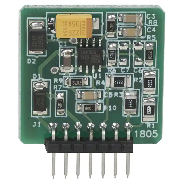
Photos
Figure 5 – IRAC1150-D2 (front and back)
Rev. 2.0
7/6/2005
International Rectifier
Page 6 of 12
�2.5
Bill of Material
IRAC1150-D2 Control Board Demo - BILL OF MATERIAL
1
2
3
4
5
6
7
8
9
10
11
12
13
14
15
16
LOCATION
U1
R7
R10
R9
R8
R1 - R4
R6
R5
C1
C2
C3
C4,C5
C6,C7
D1
D2
J1
PCB
Rev. 2.0
REV: A
SIZE:
DESCRIPTION
SO8
IR1150 Control IC
1206 SMD
51 OHM 1/4W 1%
1206 SMD
100 Ohm 1/4W 1%
1206 SMD
78.7K OHM 1/4W 1%
1206 SMD
8.87K OHM 1/4W 1%
1210 SMD
499K OHM 1/4W 1%
1206 SMD
17.8K OHM 1/4W 1%
1206 SMD
18.2K OHM 1/4 1%
1210 SMD
1.0UF 50V CERAMIC X5R
2010 SMD
22UF 35V TANTALUM TEL SMD
1206 SMD
.33UF 25V CERAMIC X7R
1206 SMD
.01UF 10% 50V X7R
N/A
NOT USED
1206 SMD
RECTIFIER Zener 18V , SMD
2010 SMD
DIODE SCHOTTKY 40V 1A SMB
Thru Hole
CONN HEADER 7POS.100 RA TIN
IRAC1150-D2 Control Board Rev A
1.15 x 1.15
7/6/2005
International Rectifier
QTY:
1
1
1
1
1
4
1
1
1
1
1
2
N/A
1
1
1/5
1
VENDOR
IR
DIGI-KEY
DIGI-KEY
DIGI-KEY
DIGI-KEY
DIGI-KEY
DIGI-KEY
DIGI-KEY
DIGI-KEY
DIGI-KEY
DIGI-KEY
DIGI-KEY
N/A
DIGI-KEY
DIGI-KEY
DIGI-KEY
Advanced
PART NUMBER
IR1150STR
311-51.0FCT-ND
311-100FCT-ND
311-78.7KFCT-ND
311-8.87KFCT-ND
P499KAACT-ND
311-17.8KFCT-ND
311-18.2KFCT-ND
PCC2234CT-ND
P11302CT-ND
PCC1889CT-ND
478-1542-1-ND
N/A
SMAZ15DICT-ND
10BQ040-ND
929835-01-36-ND
IRAC1150-D2_A
Page 7 of 12
�3 IRAC1150-D2 Control Board Integration into Existing Designs
3.1 Typical Multiplier Based System Solution
Figure 6 - Multiplier Based System Level Schematic Diagram
3.2 IRAC1150-D2 Integration into Existing Design
The IRAC1150-D2 Control Board can be integrated into SMPS designs with minor circuit
level modifications. Many components can be removed from the above design when using
the IRAC1150-D2. System performance will be maintained while the number of required
components and pcb space will be greatly reduced. The IRAC1150-D2 Control Board is
integrated into the existing design as shown below in Figure 7. The board is designed for a
VCC range of 14VDC to 20VDC.
Figure 7 - IRAC1150-D2 Control Board Integrated into Existing Design
Rev. 2.0
7/6/2005
International Rectifier
Page 8 of 12
�3.2.1 Output Voltage Dividers
The IRAC1150-D2 provides voltage divider strings for both the output voltage error
amplifier and the overvoltage protection comparator on-board, so pin 7 is connected to
the output of the converter as shown in Fig. 7. In designs where resistor divider strings
are present on the motherboard, the IRAC1150-D2 can be modified according to the
following, (ref schematic Fig.1). Output voltage is set for a nominal 390VDC.
Output Voltage Error Amplifier Divider
•
Designs with entire divider string located on motherboard – Replace R1 and R2
with 0 ohm jumper, remove R5, and connect pin 7 to junction of divider string
that normally connects to input of error amplifier of existing control board.
Resistor values may change due to differences in reference voltages
between the two controllers. Refer to IR1150S Data Sheet, (PD60230).
•
Designs with the bottom resistor of divider located on Control Board - Replace
R1 and R2 with 0 ohm jumper and connect pin 7 to junction of divider string that
normally connects to input of error amplifier of existing control board. Resistor
R5 value may be required to change depending on resistor values on
motherboard in order to maintain the same output voltage as existing design.
Over Voltage Comparator Divider
Rev. 2.0
•
Designs with entire divider string located on Mother Board – Remove R3, R4,
and R6, connect pin 5 to junction of divider string that normally connects to
input of over voltage comparator on existing control board. Resistor values
may change due to differences in reference voltages between the two
controllers. Refer to IR1150S Data Sheet, (PD60230).
•
Designs with bottom resistor of divider located on Control Board - Remove R3
and R4 then connect pin 5 to junction of divider string that normally connects to
the input overvoltage comparator of existing control board. Resistor R6 value
may be required to change depending on resistor values on Mother Board in
order to maintain same OVP threshold as existing design.
7/6/2005
International Rectifier
Page 9 of 12
�3.2.2 Switching Frequency
The switching frequency of the IRAC1150-D2 Control Board is user programmable.
The default setting is 100kHz and can be changed by removing R9 (schematic, Fig.1)
and replacing it with a value from the chart in Fig. 8, corresponding to the desired
switching frequency. The IR1150 controller has a frequency range of 50 – 200kHz.
Figure 8 - Switching Frequency vs. Programming Resistor Value
3.2.3 Current Sense Resistor
Detailed design of the current sense resistor value can be found in the IR1150S
Application Note AN-1077. Calculated values for a universal input converter with an
85VAC low line for typical output power levels is shown below in Table 1 (see
assumptions below). Typically, the closest standard value would be selected and the
calculations run again in order to optimize the system.
Output Power Level, (Watts) Current Sense Resistor Value, (Ohms)
150
0.227
300
0.114
500
0.068
750
0.045
1000
0.034
Table 1 - Calculated Current Sense Resistor Values for Given Output Power Levels
Note: Assumes a converter overload factor of 10%, ∆IL = 20%, converter minimum
efficiency of 92% at low line of 85VAC, and converter output voltage of 385VDC.
Rev. 2.0
7/6/2005
International Rectifier
Page 10 of 12
�3.2.4 Output Voltage Loop Compensation
The loop compensation provided for on the IRAC1150-D2 Control Board provides the
frequency response shown below in Fig. 9. It provides for stable operation, good
power factor and THD with a 28Hz crossover frequency, while providing a soft start
time of approximately 40msec. The compensation should suffice for most all systems,
however detailed compensation design criteria is discussed in Application Note AN1077.
48.97
50
0
20⋅ log( H ( 1j⋅ ω n)
)
50
− 60.402 100
0
0.1
0.1
1
0.1
0.1
1
10
1 .10
100
3
1 .10
4
1 .10
5
fn
1 .10
1×10
6
6
0
10
20
30
arg( H( 1j⋅ ω n) )
40
deg
50
60
70
80
− 90 90
10
1 .10
3
100
1 .10
4
fn
1 .10
5
1 .10
1×10
6
6
Figure 9 - Voltage Loop Gain and Phase Plots
Rev. 2.0
7/6/2005
International Rectifier
Page 11 of 12
�3.3 Design Tips for Optimized Operation
•
Minimize gate drive current loop - Ground pin of IC, current sense resistor, and
source of power switch should be as close to a single node as practically possible. A
star point connection, although not always practical in real world pcb layout, is
optimum.
single connection point
minimize this loop area
Figure 10 – Connection of Power Switch Source, Current Sense Resistor, and IC Ground
•
The IRAC1150-D2 provides a robust 1.5A peak gate current. Optimization of gate
drive resistors is required to achieve optimum performance in terms of system noise,
EMI and efficiency. Match the drive circuit to the power switch and system
requirements – e.g. the larger IRAC1150-300W Demo Board employs an
IRFP27N60K power switch. The turn-on resistance is 8.9Ω and the turn off resistance
is 2.7Ω. This offers a good compromise between switching losses and EMI. The
gate resistors selected will depend upon the desired system level performance, the
power switch selection, the boost diode selection, etc. Please refer to application
notes available on the International Rectifier website which address gate drive design
and optimization.
•
An additional feature of the IRAC1150-D2 is the OVP/EN function, (pin 5), which is
shown in the circuit of Figure 7 as not connected. This pin can be brought out into
the circuit in order to initiate “sleep mode” feature of the IR1150S control IC.
Rev. 2.0
7/6/2005
International Rectifier
Page 12 of 12
�