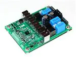
IRAUDAMP11
120W x 3 Channel Class D Audio Power Amplifier
Using the IRS2053M and IRF6665
By
Jun Honda, Liwei Zheng
CAUTION:
International Rectifier suggests the following guidelines for safe operation and handling of
IRAUDAMP11 Demo board;
Always wear safety glasses whenever operating Demo Board
Avoid personal contact with exposed metal surfaces when operating Demo Board
Turn off Demo Board when placing or removing measurement probes
www.irf.com
IRAUDAMP11 REV 1.0
Page 1 of 35
�TABLE OF CONTENTS
PAGE
INTRODUCTION............................................................................................................................................... 3
SPECIFICATIONS ............................................................................................................................................ 3
CONNECTION SETUP ..................................................................................................................................... 5
CONNECTOR DESCRIPTION ......................................................................................................................... 5
TEST PROCEDURES....................................................................................................................................... 6
PERFORMANCE AND TEST GRAPHS .......................................................................................................... 7
CLIPPING CHARACTERISTICS.................................................................................................................... 10
SOFT CLIPPING............................................................................................................................................. 10
EFFICIENCY................................................................................................................................................... 12
THERMAL CONSIDERATIONS ..................................................................................................................... 12
THERMAL INTERFACE MATERIAL’S PRESSURE CONTROL ................................................................................. 13
POWER SUPPLY REJECTION RATIO (PSRR)............................................................................................ 15
SHORT CIRCUIT PROTECTION RESPONSE .............................................................................................. 16
IRAUDAMP11 OVERVIEW ............................................................................................................................ 17
FUNCTIONAL DESCRIPTIONS..................................................................................................................... 19
IRS2053 GATE DRIVER IC ............................................................................................................................ 19
SELF-OSCILLATING FREQUENCY .................................................................................................................... 20
ADJUSTMENTS OF SELF-OSCILLATING FREQUENCY ......................................................................................... 20
SELECTABLE DEAD-TIME ................................................................................................................................ 21
PROTECTION SYSTEM OVERVIEW ............................................................................................................ 22
CLICK AND POP NOISE REDUCTION ......................................................................................................... 24
BUS PUMPING............................................................................................................................................... 24
INPUT SIGNAL AND GAIN SETTING ........................................................................................................... 26
GAIN SETTING............................................................................................................................................... 26
IRAUDAMP11 FABRICATION MATERIALS................................................................................................. 28
IRAUDAMP11 HARDWARE .......................................................................................................................... 31
IRAUDAMP11 PCB SPECIFICATIONS......................................................................................................... 32
REVISION CHANGES DESCRIPTIONS........................................................................................................ 35
www.irf.com
IRAUDAMP11 REV 1.0
Page 2 of 35
�Introduction
The IRAUDAMP11 Demo board is a reference design which uses only one IC (IRS2053M) to derive
appropriate input signals, amplify the audio input, and achieve a three-channel 120 W/ch (4Ω, THD+N=1%)
half-bridge Class D audio power amplifier. The reference design demonstrates how to use the IRS2053M
Class D audio controller and gate driver IC, implement protection circuits, and design an optimum PCB
layout using IRF6665 DirectFET MOSFETs. The reference design contains all the required housekeeping
power supplies for ease of use. The three-channel design is scalable, for power and number of channels.
Applications
AV receivers
Home theater systems
Mini component stereos
Powered speakers
Sub-woofers
Musical Instrument amplifiers
Automotive after market amplifiers
Features
Output Power:
Residual Noise:
Distortion:
Efficiency:
Multiple Protection Features:
PWM Modulator:
120W x 3 channels (4Ω, THD+N=1%)
or 170W x 3 channels (4Ω, THD+N=10%)
220V, IHF-A weighted, AES-17 filter
0.02% THD+N @ 60W, 4Ω
90% @ 120W, 4Ω, single-channel driven, Class D stage
Over-current protection (OCP), high side and low side
Over-voltage protection (OVP),
Under-voltage protection (UVP), high side and low side
Over-temperature protection (OTP)
Self-oscillating half-bridge topology with optional clock synchronization
Specifications
General Test Conditions (unless otherwise noted)
Supply Voltages
±35V
Load Impedance
4Ω
Self-Oscillating Frequency
400kHz
Gain Setting
28dB
Notes / Conditions
No input signal, Adjustable
1Vrms input yields rated power
Electrical Data
IR Devices Used
Typical
Notes / Conditions
IRS2053M Audio Controller and Gate-Driver,
IRF6665 DirectFET MOSFETs
Modulator
Self-oscillating, second order sigma-delta modulation, analog input
Power Supply Range
± 25V to ±35V
Bipolar power supply
Output Power CH1-3: (1% THD+N)
120W
1kHz, ±35V
Output Power CH1-3: (10% THD+N)
170W
1kHz, ±35V
www.irf.com
IRAUDAMP11 REV 1.0
Page 3 of 35
�Rated Load Impedance
Standby Supply Current
Total Idle Power Consumption
Channel Efficiency
8-4Ω
+75/-95mA
6W
90%
Resistive load
No input signal
No input signal
Single-channel driven,
120W, Class D stage
.
Audio Performance
Class D
Output
THD+N, 1W
THD+N, 10W
THD+N, 60W
THD+N, 100W
0.015%
0.01%
0.02%
0.03%
Dynamic Range
101dB
Residual Noise, 22Hz - 20kHzAES17
220V
Damping Factor
Channel Separation
67
75dB
75dB
70dB
±1dB
±3dB
Frequency Response : 20Hz-20kHz
: 20Hz-35kHz
Physical Specifications
Dimensions
Notes / Conditions
1kHz, Single-channel driven
A-weighted, AES-17 filter,
Single-channel operation
Self-oscillating – 400kHz
1kHz, relative to 4Ω load
100Hz
1kHz
10kHz
1W, 4Ω - 8Ω Load
Weight
3.94”(L) x 2.83”(W) x 0.85”(H)
100 mm (L) x 72 mm (W) x 21.5 mm(H)
0.130kgm
www.irf.com
IRAUDAMP11 REV 1.0
Page 4 of 35
�Connection Setup
Audio Signal Generator
CH1 CH2 CH3
Input
Frequency adjustor
VR1
DS1
VCC INDICATOR
IRS2053M
IRF6665
Output
Output
CH2 CH1 +B GND -B CH3
G
35 V, 5 A DC supply
250W, 4Ω,
Non-inductive Resistors
35 V, 5 A DC supply
Fig 1 Typical Test Setup
Connector Description
CH1 IN
CH2 IN
CH3 IN
SUPPLY
CH1 OUT
CH2 OUT
CH3 OUT
www.irf.com
CN1
CN1
CN1
P1
P2
P2
P3
Analog input for CH1
Analog input for CH2
Analog input for CH3
Positive and negative supply (+B / -B)
Output for CH1
Output for CH2
Output for CH3
IRAUDAMP11 REV 1.0
Page 5 of 35
�Test Procedures
Test Setup:
1. Connect 4-200 W dummy loads to 3 output connectors (P2 and P3 as shown on Fig 1)
and an Audio Precision analyzer (AP).
2. Connect the Audio Signal Generator to CN1 for CH1~CH3 respectively (AP).
3. Set up the dual power supply with voltages of ±35V; current limit to 5A.
4. TURN OFF the dual power supply before connecting to On of the unit under test (UUT).
5. Connect the dual power supply to P1. as shown on Fig 1
Power up:
6. Turn ON the dual power supply. The ±B supplies must be applied and removed at the
same time.
7. The Blue LED should turn ON immediately and stay ON
8. Quiescent current for the positive supply should be 75mA 10mA at +35V.
9. Quiescent current for the negative supply should be 95mA 10mA at –35V.
Switching Frequency test
10. With an Oscilloscope, monitor the switching waveform at test points VS1~VS3. Adjust VR1
to set the self oscillating frequency to 400 kHz 25 kHz when DUT in clock synchronize
mode.
Functionality Audio Tests:
11. Set the signal generator to 1kHz, 20 mVRMS output.
12. Connect the audio signal generator to CN1(Input of CH1,CH2,CH3)
13. Sweep the audio signal voltage from 15 mVRMS to 1 VRMS.
14. Monitor the output signals at P2/P3 with an oscilloscope. The waveform must be a non
distorted sinusoidal signal.
15. Observe that a 1 VRMS input generates an output voltage of 25.52 VRMS(CH1/CH2). The
ratio, R4x/(R3x) and R30x/(R31x), determines the voltage gain of IRAUDAMP11.
Test Setup using Audio Precision (Ap):
16. Use an unbalanced-floating signal from the generator outputs.
17. Use balanced inputs taken across output terminals, P2 and P3.
18. Connect Ap frame ground to GND at terminal P1.
19. Select the AES-17 filter(pull-down menu) for all the testing except frequency response.
20. Use a signal voltage sweep range from 15 mVRMS to 1 VRMS.
21. Run Ap test programs for all subsequent tests as shown in Fig 2- Fig 7below.
www.irf.com
IRAUDAMP11 REV 1.0
Page 6 of 35
�Performance and test graphs
10
5
2
1
0.5
0.2
0.1
%
0.05
0.02
0.01
0.005
0.002
0.001
100m
200m
500m
1
2
5
10
20
50
100
200
W
S weep
Trac e
Color
Line S ty le
Thic k
Data
A x is
Com m ent
1
1
2
1
3
3
Red
B lue
G reen
S olid
S olid
S olid
2
2
2
A nlr.THD+ N Ratio
A nlr.THD+ N Ratio
A nlr.THD+ N Ratio
Left
Left
Left
CH1
CH2
±B Supply = ±35V, 4 Ω Resistive Load
Fig 2 IRAUDAMP11, THD+N versus Power, Stereo, 4 Ω
.
+4
T
+3
+2
+1
-0
-1
d
B
r
-2
A
-4
-3
-5
-6
-7
-8
-9
-10
20
50
100
200
500
1k
2k
5k
10k
20k
50k
100k 200k
Hz
CH1-Blue; CH2-Yellow; CH3-Red
±B Supply = ±35V, 4 Ω Resistive Load
Fig 3 IRAUDAMP11, Frequency response
www.irf.com
IRAUDAMP11 REV 1.0
Page 7 of 35
�Red
Blue
CH1, 10W Output
CH1, 50W Output
Fig 4 THD+N Ratio vs. Frequency
+0
-20
d
B
V
-40
-60
-80
-100
20
50
100
200
500
1k
2k
5k
10k
Hz
Sweep
Trace
Color
Line Style
1
1
2
1
2
1
Yellow Solid
Blue
Solid
Red
Solid
Thick
Data
Axis
Comment
2
2
2
Fft.Ch.1 Ampl
Fft.Ch.2 Ampl
Fft.Ch.1 Ampl
Left
Left
Left
CH2
CH3
CH1
Fig 5, 1V output Frequency Spectrum
www.irf.com
IRAUDAMP11 REV 1.0
Page 8 of 35
20k
�+0
-25
d
B
V
-50
-75
-100
-125
-150
10
20
50
100
200
500
1k
2k
5k
10k
20k
Hz
Sweep
Trace
Color
Line Style
Thick
Data
Axis
Comment
1
1
2
1
2
1
Red
Blue
Yellow
Solid
Solid
Solid
2
2
2
Fft.Ch.1 Ampl
Fft.Ch.2 Ampl
Fft.Ch.1 Ampl
Left
Left
Left
CH1
CH3
CH2
No signal, Self Oscillator @ 400kHz
Fig 6, IRAUDAMP11 Noise Floor
.
+0
-1 0
-2 0
-3 0
d
B
r
-4 0
A
-6 0
-5 0
-7 0
-8 0
-9 0
-1 0 0
20
50
100
200
500
1k
2k
5k
10k
20k
Hz
S weep
Tra c e
C o lo r
L in e S t y le
Th ic k
D ata
A x is
Com m ent
1
3
4
5
6
7
1
1
1
1
1
1
Cy an
Y e llo w
Red
M agenta
B lu e
Cy an
S o lid
S o lid
S o lid
S o lid
S o lid
S o lid
2
2
2
2
1
1
A n lr. A m p l
A n lr. A m p l
A n lr. A m p l
A n lr. A m p l
A n lr. A m p l
A n lr. A m p l
L e ft
L e ft
L e ft
L e ft
L e ft
L e ft
C H 3 _ o n ; C H 1 _ o ff
C H 1 _ o n ; C H 3 _ o ff
C H 2 _ o n ; C H 3 _ o ff
C H 3 _ o n ; C H 2 _ o ff
C H 2 _ o n ; C H 1 _ o ff
C h 1 _ o n ; C H 2 _ o ff
Fig 7, Channel separation vs. frequency
www.irf.com
IRAUDAMP11 REV 1.0
Page 9 of 35
�Clipping characteristics
Red Trace: Total Distortion + Noise Voltage
Green Trace: Output Voltage
60W / 4, 1kHz, THD+N=0.02%
174W / 4, 1kHz, THD+N=10%
Measured Output and Distortion Waveforms(CH1/CH2)
Fig 8 Clipping Characteristics
.
Soft Clipping
IRS2053M has Clipping detection function, it monitors error voltage in COMP pin with a window
comparator and pull an open drain nmos referenced to GND. Threshold to detect is at 10% and
90% of VAA-VSS. Each channel has independent CLIP outputs. Once IRS2053M detects
Clipping, the CLIP pin will generate pulses to trigger soft clipping circuit as Fig 9, which limits
output’s maximum power.
Fig10 shows 20Hz and 20 kHz THD+N versus Power graph in CH3; it shows limitation of output’s
power with different frequency.
www.irf.com
IRAUDAMP11 REV 1.0
Page 10 of 35
�Soft Clipping
R28A
1K
C15A
10uF, 16V
C6A
1uF,50V
R5A
47K
R29A
220K
D3A
1N4148
Audio signal INPUT
C0A
R7A
470K
GND
R6A
47K
CLIP Detection
D
R27A
Q5
VAA
DTA144EKA
10uF,50V 3.3K
G
R3A
S
Q6
MMBFJ112
1K
IN-
C5A
10uF, 50V
VSS
GND
Fig 9 Soft Clipping Circuit
10
5
2
1
0.5
0.2
%
0.1
0.05
0.02
0.01
0.005
0.002
0.001
100m
200m
500m
1
2
5
10
20
50
100
300
W
Sweep
Trace
Color
Line Style
Thick
Data
Axis
Comment
1
2
1
1
Red
Blue
Solid
Solid
2
2
Anlr.THD+N Ratio
Anlr.THD+N Ratio
Left
Left
20Hz
20kHz
±B Supply = ±35V, 4 Ω Resistive Load
Fig 10 IRAUDAMP11/CH3, THD+N versus Power, Stereo, 4 Ω
www.irf.com
IRAUDAMP11 REV 1.0
Page 11 of 35
�Efficiency
Fig 11 shows efficiency characteristics of the IRAUDAMP11. The high efficiency is achieved by
following major factors:
1) Low conduction loss due to the DirectFETs offering low RDS(ON)
2) Low switching loss due to the DirectFETs offering low input capacitance for fast rise and
fall times
Secure dead-time provided by the IRS2053M, avoiding cross-conduction.
Efficiency (%)
100%
90%
Efficiency (%)
80%
70%
60%
AMP11 35V 4ohms
50%
40%
30%
20%
10%
0%
0
50
100
150
Output power (W)
Fig 11, IRAUDAMP11 4 ohms load Stereo, ±B supply = ±35V
Thermal Considerations
With this high efficiency, the IRAUDAMP11 design can handle one-eighth of the continuous rated
power, which is generally considered to be a normal operating condition for safety standards,
without additional heatsinks or forced air-cooling.
www.irf.com
IRAUDAMP11 REV 1.0
Page 12 of 35
�Thermal Interface Material’s Pressure Control
The pressure between DirectFET & TIM (Thermal Interface Material) is controlled by depth of Heat
Spreader’s groove. Choose TIM which is recommended by IR. (Refer to AN-1035 for more
details). TIM’s manufacturer thickness, conductivity, & etc. determine pressure requirement.
Below shows selection options recommended:
Fig 12 TIM Information
www.irf.com
IRAUDAMP11 REV 1.0
Page 13 of 35
�Check the TIM’s compression deflection with constant rate of strain (example as Fig.13) base on
manufacturer’s datasheet. According to the stress requirement, find strain range for the TIM. Then,
calculate heat spreader groove depth as below:
Groove Depth=DirectFET’s Height +TIM’s Thickness*strain
**DirectFET’s height should be measured from PCB to the top of DirectFET after reflow. The
average height of IRF6665 is 0.6mm.
Fig 13 compression deflection with constant rate of strain
www.irf.com
IRAUDAMP11 REV 1.0
Page 14 of 35
�Power Supply Rejection Ratio (PSRR)
The IRAUDAMP11 obtains good power supply rejection ratio of -68 dB at 1kHz shown in Fig 14.
With this high PSRR, IRAUDAMP11 accepts any power supply topology when the supply voltages
fit between the min and max range.
+0
-10
-20
-30
d
B
V
-40
-50
-60
-70
-80
-90
20
50
100
200
500
1k
2k
5k
10k
20k
40k
Hz
Sweep
Trace
Color
Line Style
Thick
Data
Axis
1
1
Magenta
Solid
2
Anlr.Ampl
Left
Comment
Fig 14 Power Supply Rejection Ratio (PSRR)
www.irf.com
IRAUDAMP11 REV 1.0
Page 15 of 35
�Short Circuit Protection Response
Figs 15-16 show over current protection reaction time of the IRAUDAMP11 in a short circuit event.
As soon as the IRS2053M detects an over current condition, it shuts down PWM. After one
second, the IRS2053M tries to resume the PWM. If the short circuit persists, the IRS2053M
repeats try and fail sequences until the short circuit is removed.
Short Circuit in Positive and Negative Load Current
CSD pin
CSD pin
VS pin
VS pin
Load current
Load current
Positive OCP
Negative OCP
Fig 15 Positive and Negative OCP Waveforms
.
OCP Waveforms Showing CSD Trip and Hiccup
CSD pin
CSD pin
VS pin
VS pin
Load current
Load current
Fig 16 OCP Response with Continuous Short Circuit
www.irf.com
IRAUDAMP11 REV 1.0
Page 16 of 35
�IRAUDAMP11 Overview
The IRAUDAMP11 features a 3CH self-oscillating type PWM modulator for the smallest space,
highest performance and robust design. This topology represents an analog version of a secondorder sigma-delta modulation having a Class D switching stage inside the loop. The benefit of the
sigma-delta modulation, in comparison to the carrier-signal based modulation, is that all the error
in the audible frequency range is shifted to the inaudible upper-frequency range by nature of its
operation. Also, sigma-delta modulation allows a designer to apply a sufficient amount of error
correction.
The IRAUDAMP11 self-oscillating topology consists of following essential functional blocks.
Front-end integrator
PWM comparator
Level shifters
Gate drivers and MOSFETs
Output LPF
Integrator
Referring to Fig 17 below, the input operational amplifier of the IRS2053M forms a front-end
second-order integrator with R3x, C2x, C3x, and R2x. The integrator that receives a rectangular
feedback signal from the PWM output via R4x and audio input signal via R3x generates a
quadratic carrier signal at the COMP pin. The analog input signal shifts the average value of the
quadratic waveform such that the duty cycle varies according to the instantaneous voltage of the
analog input signal.
PWM Comparator
The carrier signal at the COMP pin is converted to a PWM signal by an internal comparator that
has a threshold at middle point between VAA and VSS. The comparator has no hysteresis in its
input threshold.
Level Shifters
The internal input level-shifter transfers the PWM signal down to the low-side gate driver section.
The gate driver section has another level-shifter that level shifts up the high-side gate signal to the
high-side gate driver section.
www.irf.com
IRAUDAMP11 REV 1.0
Page 17 of 35
�Gate Drivers and DirectFETs
The received PWM signal is sent to the dead-time generation block where a programmable
amount of dead time is added into the PWM signal between the two gate output signals of LO and
HO to prevent potential cross conduction across the output power DirectFETs. The high-side levelshifter shifts up the high-side gate drive signal out of the dead-time block.
Each channel of the IRS2053M’s drives two DirectFETs, high- and low-sides, in the power stage
providing the amplified PWM waveform.
Output LPF
The amplified PWM output is reconstructed back to an analog signal by the output LC LPF.
Demodulation LC low-pass filter (LPF) formed by L1 and C13, filters out the Class D switching
carrier signal leaving the audio output at the speaker load. A single stage output filter can be used
with switching frequencies of 400 kHz and greater; a design with a lower switching frequency may
require an additional stage of LPF.
Fig 17 Simplified Block Diagram of IRAUDAMP11 Class D Amplifier
www.irf.com
IRAUDAMP11 REV 1.0
Page 18 of 35
�Functional Descriptions
IRS2053M Gate Driver IC
The IRAUDAMP11 uses the IRS2053M, a 3 Channel high-voltage (up to 200 V), high-speed
power MOSFET driver with internal dead-time and protection functions specifically designed for
Class D audio amplifier applications. These functions include OCP and UVP. The IRS2053M
integrates bi-directional over current protection for both high-side and low-side MOSFETs. The
dead-time can be selected for optimized performance according to the size of the MOSFET,
minimizing dead-time while preventing shoot-through. As a result, there is no gate-timing
adjustment required externally. Selectable dead-time through the DT pin voltage is an easy and
reliable function which requires only two external resistors, R12 and R13 as shown on Fig 18 or
Fig 24 below.
The IRS2053M offers the following functions.
PWM modulator
Dead-time insertion
Over current protection
Under voltage protection
Level shifters
Refer to IRS2053M datasheet and AN-1158 for more details.
L1A
CH3 OUTPUT
D4
1N4148
R4 0R0 or N/A
D1C
SD
R15B
10K
R18B
R17B
10K
R16B
3.9K
VAA
+5v
0.1uF,100V
5
4
C41
N/A
2
3
4
1A VCC
1B
1Y
2Y
2B
GND 2A
R43
R47
330R,1W
R45
330R,1W
R51
10k Z7
R52
10k
R21A
0.1uF, 63V 10R,1W
C14A
0.1uF, 63V
39V
Z8
R25A
100K
R25B
100K
39V
R25C
OVP
-B
100K
CH1 OUTPUT
P2
CH1 OUTPUT
GND
GND
CH2 OUTPUT
R46
8
-5v
1
2
3
4
CH2 OUTPUT
ZX5T953
33k
R44
4CH2
3
2
1CH1
510R,1W
Z2
R36
7
R54
10k
6
R57
47k
R56
47k
5
5.1k
Z4
18V
Q3
MMBT5551
DS1
R58
47k
R55
47k
OVP
L5
220uH
C35
2.2nF,50V
R31
5.1k
Q4
MMBT5551
0.01uF, 50V
15V
R37
47k
IC9
VCC
R50
47k
Z3
39V R53
10k
R61
0.1uF, 63V
GND
GND
CH3 OUTPUT
CH3 OUTPUT
IC8
TC7W00FFCT-ND
C61
C14C
P3
1N4148
Z6
5.6V
Q9
1
-B
D1B
R42
3.3k
C37
22uF, 16V
VCC OUT
GND
SET DIT
C17B
1000uF,35V
R12C
N/A
Z5
5.6V
C40
N/A
IC2
LTC1799
1
2
3
R21B
10R,1W
GND
R23B
100k
C17D
0.1uF,50V
22R
4.7R
33k
VR1
10K
C17A
1000uF,35V
+B
Q8 ZX5T853
0.1uF,50V
R3
22k
R21C
10R,1W
0.47uF, 400V
C13A
1R
1R
R19B
R19C
Q2C
IRF6665
R23A
100k
C17C
0.1uF,50V
R12B
N/A
R22B 10K
C1
C14B
+B
Q1C
IRF6665
R9C
D2B
1N4148
0.1uF,50V
0.47uF, 400V
C13C
Q2B
IRF6665
22R
22R
C19B
VS1
R9B
R20C
DSA DSB DSC PROT
C10B
0.47uF, 400V
C13B
C19A R19A
D1A 1N4148
4.7R
R16C
3.9K
R17C
R15C 10K
10K
12
NC
VS2
HO2
VB2
9
8
11
0.1uF,50V
0
-B
R22C
10K
25
C10A
0.1uF,50V
26
NC
VS3
OTP1
OTP2
VCC
COM
OTP3
DT
VREF
HO3
1N4148
13
0.1uF,100V
C8
10uF, 16V
R4C
100K 1%
R4B
100K 1%
CH1 OUTPUT
14
HO1
GND
22R
C19C
CSD
2.2K
Q1B
IRF6665
R18C
1N4148
0R0 or N/A
2.2K
R24C
CH2 OUTPUT
L1C
22uH
D2C
VB1
10
CSD
R22
10R
GND
R24B
22uH
R20B
15
CSH1
COMP1
48
GND
4.7R
17
16
C10C
47
L1B
C9B
10uF,16V
R14B
19
LO2
IN1
1nF,50V
CSH2
C3C
2.2nF,50V
1N4148 4.7R
18
NC
NC
C4C
120R
R32
1k
R49 10R
C34
0.01uF, 25V
R41
120k
C36
0.01uF, 50V
Q1
1
2
3
4
D7
R40
100k
SW
VIN
BST
VCC
RCL
RON/SD
RTN
FB
8
7
Q2
R39
100k
6
MMBT5401
FX491
5
P1
C32
2.2uF, 50V
LM5007
C33
0.1uF, 50V
Z1
24V
R38
10R
+B
GND
-B
3
2
1
UVP
10k
C62
0.01uF, 50V
R62 10k
GND
GND
For EMI
Fig 18 System-level View of IRAUDAMP11
www.irf.com
2.2K
20
LO1
DCP
R2C
2.2nF,50V
R18A
D2A
21
VCC2
COMP2
46
R1
-B
3.9K
22
LO3
COM2
IN2
7
C2C
VAA
45
6
100pF, 50V
C3B
2.2nF,50V
FAULT
10uF, 16V
R1C
22K
C1C
2.2nF,50V
1nF,50V
VSS
VAA
43
4.7uF,10V
44
C4B
Q2A
IRF6665
22R
R15A
10K R17A
10K
R16A
24
23
NC
5
120R
100pF, 50V
R3C
5.6K
C5C
R2B
OCSET
NC
C2B
C7
22R
R9A
IC1
R12A
N/A
1R
95C
Q1A
IRF6665
R20A
0.1uF,100V
RpC
R22A
10K
C16B
0.01uF
C16C
0.01uF
10R
27
28
29
NC
C16A
0.01uF
1K
C9A
10uF,16V
R13
31
30
2.2K
35
33
36
R32C
100uF,4V
R15
10R
95C
IRS2053
C9
C11
4.7uF,10V
RpB
VB3
GND
VSS
42
CLIP1
4.7uF,10V
GND
R14
10R
R7 10R
5.6K
10uF, 16V
R1B
22K
4.7uF,10V
CLIP2
C1B
CH1 INPUT
C10
GND
10R
GND
41
C6
CLIP3
220pF
R32B
CSH3
4
C5B
R30C 15K
RpA 95C
IN3
40
R3B
10K
C12C
10uF, 16V
R6 10R
TLC084
R31C
10R
COMP3
39
G
CH2 INPUT
DS
38
3
C5A
C4A
1nF,50V
2
8 GND
9
10
11
12
13
14
R2A 120R
1K
1
GND
3OUT
3IN3IN+
GND
4IN+
4IN4OUT
R3A
10K
GND
2OUT
2IN2IN+
VDD
1IN+
1IN1OUT
37
C3A 2.2nF,50V
22K
100pF, 50V
R104
IC3
7
6
5
4
3
2
1
GND
C2A 2.2nF,50V
C1A
R24A
GND
R32A
GND
47K
R26C 10K
15K
C12B
GND
220pF
1N4148
CH3 INPUT
3.3K
1N4148
10K
CN1
CH3 6
GND 5
GND 4
CH2 3
GND 2
CH1 1
10uF, 16V
R1A
R27A
R26B 10K
R30B
D3
R30A 10K
R31B
47K
1uF,50V
D3A
R6A
470K
C15A
R29A
220K
R31A 10K
MMBFJ112 Q6
S
D
220pF
R26A 10K
GND
C12A
R4A
100K 1%
R5A
34
DTA144EKA
R11 8.2K
1K
C6A
R7A
R12
Q5
32
R28A
R10
22uH
R14A 4.7R
IRAUDAMP11 REV 1.0
Page 19 of 35
�Self-Oscillating Frequency
Self-oscillating frequency is determined by the total delay time along the control loop of the
system; the propagation delay of the IRS2053M, the DirectFETs switching speed, the timeconstant of front-end integrator (R2, R3, R4, C2, C3 ). Variations in +B and –B supply voltages
also affect the self-oscillating frequency.
The self-oscillating frequency changes with the duty ratio. The frequency is highest at idling. It
drops as duty cycle varies away from 50%.
Adjustments of Self-Oscillating Frequency
Use R2 to set different self-oscillating frequencies. The PWM switching frequency in this type of
self-oscillating switching scheme greatly impacts the audio performance, both in absolute
frequency and frequency relative to the other channels. In absolute terms, at higher frequencies,
distortion due to switching-time becomes significant, while at lower frequencies, the bandwidth of
the amplifier suffers. In relative terms, interference between channels is most significant if the
relative frequency difference is within the audible range.
Normally, when adjusting the self-oscillating frequency of the different channels, it is suggested to
either match the frequencies accurately, or have them separated by at least 25kHz. Under the
normal operating condition with no audio input signal, the switching-frequency is set around
400kHz in the IRAUDAMP11.
www.irf.com
IRAUDAMP11 REV 1.0
Page 20 of 35
�Selectable Dead-time
The dead-time of the IRS2053 is set based on the voltage applied to the DT pin. Fig 19 lists the
suggested component value for each programmable dead-time between 45 and 105 ns.
All the IRAUDAMP11 models use DT1 (45ns) dead-time.
Dead-time Mode
DT1
DT2
DT3
DT4
R1