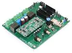
IRAUDAMP4A
120 W x 2 Channel Class D Audio Power Amplifier
Using IRS20957 and IRF6645
By
Johan Strydom, Jun Honda, and Jorge Cerezo
Table of Contents
Page
Introduction .......................................................................................... 1
Specifications ....................................................................................... 2
Functional Description.......................................................................... 4
Startup and Shutdown..........................................................................12
Protection .............................................................................................16
Typical Performance ............................................................................21
Design Documents ..............................................................................27
CAUTION: International Rectifier suggests the following guidelines for
safe operation and handling of IRAUDAMP4A Demo Board;
• Always wear safety glasses whenever operating Demo Board
• Avoid personal contact with exposed metal surfaces when operating
Demo Board
• Turn off Demo Board when placing or removing measurement probes
www.irf.com
IRAUDAMP4A
�Introduction
The IRAUDAMP4A reference design is an example of a two-channel 120 W half-bridge
Class D audio power amplifier. The reference design will demonstrate how to use the
IRS20957, implement protection circuits, and design an optimum PCB layout using the
IRF6645 DirectFET MOSFETs. The resulting design requires no heatsink for normal
operation (one-eighth of continuous rated power). The reference design contains all the
required housekeeping power supplies for ease of use. The two-channel design is
scalable, for power and the number of channels.
Applications
AV receivers
Home theater systems
Mini component stereos
Sub-woofers
Features
Output Power:
120 W x two channels,
Total Harmonic Distortion (THD) = 1%, 1 kHz
Residual Noise:
52 µV, IHF-A weighted, AES-17 filter
Distortion:
0.004% THD+N @ 60 W, 4 Ω
Efficiency:
96% @ 120 W, 4 Ω, single-channel driven, Class D stage
Multiple Protection Features: Over-current protection (OCP),
Over-voltage protection (OVP),
Under-voltage protection (UVP),
DC-protection (DCP),
Over-temperature protection (OTP)
PWM Modulator:
Self-oscillating half-bridge topology with optional clock
synchronization
www.irf.com
IRAUDAMP4A
1
�Specifications
General Test Conditions (unless otherwise noted)
Supply Voltage
±35 V
Load Impedance
4Ω
Self-Oscillating Frequency
400 kHz
Gain Setting
26.8 dB
Notes / Conditions
No input signal
1 Vrms input yields rated power
Electrical Data
IR Devices Used
Typical
Notes / Conditions
IRS20957 gate driver,
IRF6645 DirectFET MOSFET
Modulator
Self-oscillating, second order sigma-delta modulation, analog input
Power Supply Range
± 25 - 35 V
Output Power CH1-2: (1% THD+N)
120 W
1 kHz
Output Power CH1-2: (10% THD+N)
170 W
1 kHz
Rated Load Impedance
4Ω
Supply Current
100 mA
No input signal
Total Idle Power Consumption
7W
No input signal
Single-channel driven,
Channel Efficiency
96%
120 W, Class D stage
Audio Performance
THD+N, 1 W
THD+N, 10 W
THD+N, 60 W
Typical / Class D*
0.005%
0.002%
0.002%
0.001%
0.004%
0.003%
Dynamic Range
113 dB
120 dB
70 µV
50 µV
170
95 dB
80 dB
±1 dB
±3 dB
40 µV
20 µV
2000
100 dB
85 dB
Residual Noise, 20Hz - 20 kHz BW,
A-Weighted
Damping Factor
Channel Separation
Frequency Response : 20Hz-20 kHz
: 20Hz-40 kHz
Thermal Performance
Idling
2ch x 15 W (1/8 rated power)
2ch x 120 W (rated power)
Physical Specifications
Dimensions
Typical
TC =30 °C
TPCB=37 °C
TC =54 °C
TPCB=67 °C
TC =80 °C
TPCB=106 °C
Notes / Conditions
1 kHz, Single-channel driven
A-weighted, AES-17 filter,
Single-channel operation
Self-oscillating – 400 kHz
Internal clock – 300 kHz
1 kHz, relative to 4 Ω load
100 Hz
10 kHz
1W, 4 Ω - 8 Ω Load
Notes / Conditions
No signal input, TA=25 °C
Continuous, TA=25 °C
At OTP shutdown @ 150 s,
TA=25 °C
5.8 in (L) x 5.2 in (W)
Note: Specifications are typical and not guaranteed
*Class D refers to audio performance measurements of the Class D output power stage
only, with preamp and output filter bypassed.
www.irf.com
IRAUDAMP4A
2
�Connection Diagram
35 V, 5 A DC supply
35 V, 5 A DC supply
250 W, Non-inductive Resistors
4Ω
4Ω
G
J3
CH1
Output
J4
TP1
S1
CH2
Output
J7
J9
TP2
LED
Protection
J6
CH1
Input
J8
J5
CH2
Input
Normal
S2
S3
Volume
R113
Audio Signal Generator
Figure 1. Typical Test Setup
Pin Description
CH1 IN
CH2 IN
POWER
CH1 OUT
CH2 OUT
EXT CLK
DCP OUT
J6
J5
J7
J3
J4
J8
J9
Analog input for CH1
Analog input for CH2
Positive and negative supply (+B / -B)
Output for CH1
Output for CH2
External clock sync
DC protection relay output
Power-on and Power-off Procedure
Always apply or remove ±35 V bus supplies at the same time.
www.irf.com
IRAUDAMP4A
3
�Functional Description
Class D Operation
Referring to CH1 as an example, the op-amp U1 forms a front-end second-order
integrator with C11, C13 & R25 + R29P. This integrator receives a rectangular feedback
waveform from the Class D switching stage and outputs a quadratic oscillatory waveform
as a carrier signal. To create the modulated PWM signal, the input signal shifts the
average value of this quadratic waveform (through gain relationship between R13 and
R31 + R33) so that the duty varies according to the instantaneous value of the analog
input signal. The IRS20957 input comparator processes the signal to create the required
PWM signal. This PWM signal is internally level-shifted down to the negative supply rail
where this signal is split into two signals, with opposite polarity and added deadtime, for
high-side and low-side MOSFET gate signals, respectively. The IRS20957 drives two
IRF6645 DirectFET MOSFETs in the power stage to provide the amplified PWM
waveform. The amplified analog output is re-created by demodulating the amplified
PWM. This is done by means of the LC low-pass filter (LPF) formed by L1 and C23,
which filters out the Class D switching carrier signal.
Feedback
Daughter-board
U1
Σ
+B
U1
Integrator
PWM
Modulator
and Level
Shifter
GND
LPF
IRS20957S
Gate Driver
IRF6645
Direct-FET
-B
Figure 2. Simplified Block Diagram of Class D Amplifier
Power Supplies
The IRAUDAMP4A has all the necessary housekeeping power supplies onboard and
only requires a pair of symmetric power supplies ranging from ±25 V to ±35 V (+B, GND,
-B) for operation. The internally-generated housekeeping power supplies include a ±5 V
supply for analog signal processing (preamp, etc.), while a +12 V supply (VCC),
referenced to –B, is included to supply the Class D gate-driver stage.
For the externally-applied power, a regulated power supply is preferable for performance
measurements, but not always necessary. The bus capacitors, C31 and C32 on the
motherboard, along with high-frequency bypass-caps C15-C18 on daughter board,
address the high-frequency ripple current that result from switching action. In designs
involving unregulated power supplies, the designer should place a set of bus capacitors,
having enough capacitance to handle the audio-ripple current, externally. Overall
regulation and output voltage ripple for the power supply design are not critical when
using the IRAUDAMP4A Class D amplifier as the power supply rejection ratio (PSRR) of
the IRAUDAMP4A is excellent (Figure 3).
www.irf.com
IRAUDAMP4A
4
�+0
-10
-20
-30
-40
d
B
-B
-50
+B
-60
-70
-80
-90
20
50
100
200
500
1k
2k
5k
10k
20k
40k
Hz
Figure 3. Power Supply Rejection Ratio (PSRR) for Negative (-B) and Positive (+B) Supplies
Bus Pumping
Since the IRAUDAMP4A is a half-bridge configuration, bus pumping does occur. Under
normal operation during the first half of the cycle, energy flows from one supply through
the load and into the other supply, thus causing a voltage imbalance by pumping up the
bus voltage of the receiving power supply. In the second half of the cycle, this condition
is reversed, resulting in bus pumping of the other supply.
These conditions worsen bus pumping:
–
Lower frequencies (bus-pumping duration is longer per half cycle)
–
Higher power output voltage and/or lower load impedance (more energy
transfers between supplies)
–
Smaller bus capacitors (the same energy will cause a larger voltage increase)
The IRAUDAMP4A has protection features that will shutdown the switching operation if
the bus voltage becomes too high (>40 V) or too low (11 dB overdrive.
Output Filter Design, Preamplifier and Performance
The audio performance of the IRAUDAMP4A depends on a number of different factors.
The section entitled, “Typical Performance” presents performance measurements based
on the overall system, including the preamp and output filter. While the preamp and
output filter are not part of the Class D power stage, they have a significant effect on the
overall performance.
Output filter
Since the output filter is not included in the control loop of the IRAUDAMP4A, the
reference design cannot compensate for performance deterioration due to the output
filter. Therefore, it is there important to understand what characteristics are preferable
when designing the output filter:
1) The DC resistance of the inductor should me minimized to 20 mΩ or less.
2) The linearity of the output inductor and capacitor should be high with respect to
load current and voltage.
Preamplifier
The preamp allows partial gain of the input signal, and in the IRAUDAMP4A, controls the
volume. The preamp itself will add distortion and noise to the input signal, resulting in a
gain through the Class D output stage and appearing at the output. Even a few microvolts of noise can add significantly to the output noise of the overall amplifier. In fact, the
output noise from the preamp contributes more than half of the overall noise to the
system.
It is possible to evaluate the performance without the preamp and volume control, by
moving resistors R13 and R14 to R71 and R72, respectively. This effectively bypasses
the preamp and connects the RCA inputs directly to the Class D power stage input.
Improving the selection of preamp and/or output filter, will improve the overall system
www.irf.com
IRAUDAMP4A
6
�performance to approach that of the stand-alone Class D power stage. In the “Typical
Performance” section, only limited data for the stand-alone Class D power stage is
given. For example, results for THD+N vs. Output Power are provided, utilizing a range
of different inductors. By changing the inductor and repeating this test, a designer can
quickly evaluate a particular inductor.
100
TTTTTTT
10
1
%
0.1
0.01
0.001
0.0001
100m
200m
500m
1
2
5
10
20
50
100
200
W
Figure 4. Results of THD+N vs. Output Power with Different Output Inductors
Self-Oscillating PWM Modulator
The IRAUDAMP4A Class D audio power amplifier features a self-oscillating type PWM
modulator for the lowest component count and robust design. This topology represents
an analog version of a second-order sigma-delta modulation having a Class D switching
stage inside the loop. The benefit of the sigma-delta modulation, in comparison to the
carrier-signal based modulation, is that all the error in the audible frequency range is
shifted to the inaudible upper-frequency range by nature of its operation. Also, sigmadelta modulation allows a designer to apply a sufficient amount of correction.
The self-oscillating frequency is determined by the total delay time inside the control loop
of the system. The delay of the logic circuits, the IRS20957 gate-driver propagation
delay, the IRF6645 switching speed, the time-constant of front-end integrator (e.g. R25 +
R29P, C11 and C13 for CH1) and variations in the supply voltages are critical factors of
the self-oscillating frequency. Under nominal conditions, the switching-frequency is
around 400 kHz with no audio input signal and a +/-35 V supply.
Adjustments of Self-Oscillating Frequency
The PWM switching frequency in this type of self-oscillating switching scheme greatly
impacts the audio performance, both in absolute frequency and frequency relative to the
other channels. In absolute terms, at higher frequencies, distortion due to switching-time
becomes significant, while at lower frequencies, the bandwidth of the amplifier suffers. In
relative terms, interference between channels is most significant if the relative frequency
difference is within the audible range. Normally when adjusting the self-oscillating
www.irf.com
IRAUDAMP4A
7
�frequency of the different channels, it is best to either match the frequencies accurately,
or have them separated by at least 25 kHz. With the installed components, it is possible
to change the self-oscillating frequency from about 160 kHz up to 600 kHz.
Potentiometers for adjusting self-oscillating frequency
R29P
Switching frequency for CH1*
R30P
Switching frequency for CH2*
*Adjustments have to be done at an idling condition with no signal input.
Switches and Indicators
There are three different indicators on the reference design:
– An orange LED, signifying a fault / shutdown condition when lit.
– A green LED on the motherboard, signifying conditions are normal and no fault
condition is present.
– A green LED on the daughter board, signifying there is power.
There are three switches on the reference design:
– Switch S1 is a trip and reset push-button. Pushing this button has the same effect of
a fault condition. The circuit will restart about three seconds after the shutdown
button is released.
– Switch S2 is an internal clock-sync frequency selector. This feature allows the
designer to modify the switching frequency in order to avoid AM radio interference.
With S3 is set to INT, the two settings “H” and “L” will modify the internal clock
frequency by about 20 kHz to 40 kHz, either higher “H” or lower “L.” The actual
internal frequency is set by potentiometer R113 - “INT FREQ.”
– Switch S3 is an oscillator selector. This three-position switch is selectable for
internal self-oscillator (middle position – “SELF”), or either internal (“INT”) or
external (“EXT”) clock synchronization.
Switching Frequency Lock / Synchronization Feature
For single-channel operation, the use of the self-oscillating switching scheme will yield
the best audio performance. The self-oscillating frequency, however, does change with
the duty ratio. This varying frequency can interfere with AM radio broadcasts, where a
constant-switching frequency with its harmonics shifted away from the AM carrier
frequency, is preferred. In addition to AM broadcasts, multiple channels can also reduce
audio performance at low power, and can lead to increased residual noise. Clock
frequency locking/synchronization can address these unwanted characteristics.
Please note that the switching frequency lock / synchronization feature is not possible for
all frequencies and duty ratios, and operates within a limited frequency and duty-ratio
range around the self-oscillating frequency (Figure 5).
www.irf.com
IRAUDAMP4A
8
�600
Suggested clock frequency
for maximum locking range
Locking range
Operating Frequency (kHz)
500
400
300
200
Self-oscillating frequency
100
0
10%
20%
30%
40%
50%
60%
70%
80%
90%
Duty Cycle
Figure 5. Typical Lock Frequency Range vs. PWM Duty Ratio
(Self-oscillating frequency set to 400 kHz with no input)
As illustrated by the THD+N Ratio vs. Output Power results (Figure 6) , the noise levels
increase slightly when all channels are driven (ACD) with the self oscillator, especially
below the 5 W range. Residual noise typically increases by a third or more (see
“Specifications – Audio Performance”) compared to a single-channel driven (SCD)
configuration. Locking the oscillator frequency results in lowering the residual noise to
that of a single-channel-driven system. The output power range, for which the frequencylocking is successful, depends on what the locking frequency is with respect to the selfoscillating frequency. As illustrated in Figure 6, the locking frequency is lowered (from
450 kHz to 400 kHz to 350 kHz and then 300 kHz) as the output power range (where
locking is achieved) is extended. Once locking is lost, however, the audio performance
degrades, but the increase in THD seems independent from the clock frequency.
Therefore, a 300 kHz clock frequency is recommended.
It is possible to improve the THD performance by increasing the corner frequency of the
high pass filter (HPF) (R17 and C15 for Ch1) that is used to inject the clock signal. This
drop in THD, however, comes at the cost of reducing the locking range. Resistor values
of up to 100 kΩ and capacitor values down to 10 pF can be used.
In the IRAUDAMP4A, this switching frequency lock/synchronization feature is achieved
with either an internal or external clock input (selectable through S3). If an internal (INT)
clock is selected, an internally-generated clock signal will be used, adjusted by setting
potentiometer R113 “INT FREQ.” If external (EXT) clock signal is selected, a 0 V to 5 V
square-wave (~50% duty ratio) logic signal must be applied to BNC connector J17.
www.irf.com
IRAUDAMP4A
9
�100
10
1
%
0.1 Self
Osc. (ACD)
Int. Clock @ 300 kHz
Int. Clock @ 450 kHz
0.01
Self Osc. (Single Channel Driven)
0.001
100m
200m
500m
1
2
5
10
20
50
100
200
Power (W)
Figure 6. THD+N Ratio vs. Output Power for Different Switching Frequency Lock/Synchronization
Conditions
IRS20957 Gate Driver IC
The IRAUDAMP4A uses the IRS20957, which is a high-voltage (up to 200 V), highspeed power MOSFET gate driver with internal deadtime and protection functions
specifically designed for Class D audio amplifier applications. These functions include
OCP and UVP. A bi-directional current protection feature that protects both the high-side
and low-side MOSFETs are internal to the IRS20957, and the trip levels for both
MOSFETs can be set independently. In this design, the deadtime can be selected for
optimized performance, by minimizing deadtime while limiting shoot-through. As a result,
there is no gate-timing adjustment on the board. Selectable deadtime through the DT pin
voltage is an easy and reliable function which requires only two external resistors, R11
and R9.
R11
R9
Figure 7. System-level View of Gate Driver IRS20957
www.irf.com
IRAUDAMP4A
10
�Selectable Deadtime
The IRS20957 determines its deadtime based on the voltage applied to the DT pin. An
internal comparator translates which pre-determined deadtime is being used by
comparing the DT voltage with internal reference voltages. A resistive voltage divider
from VCC sets threshold voltages for each setting, negating the need for a precise
absolute voltage to set the mode. The threshold voltages between deadtime settings are
set internally, based on different ratios of VCC as indicated in the diagram below. In order
to avoid drift from the input bias current of the DT pin, a bias current of greater than
0.5 mA is suggested for the external resistor divider circuit. Suggested values of
resistance that are used to set a deadtime are given below. Resistors with up to 5%
tolerance can be used.
Deadtime mode
DT1
DT2
DT3
DT4
Deadtime
~15 ns
~25 ns
~35 ns
~45 ns
R11