IRF3610SPbF
Applications
l High Efficiency Synchronous Rectification in SMPS
l Uninterruptible Power Supply
l High Speed Power Switching
l Hard Switched and High Frequency Circuits
HEXFET® Power MOSFET
D
G
S
VDSS
RDS(on) typ.
max.
ID
Benefits
l Improved Gate, Avalanche and Dynamic dV/dt
Ruggedness
l Fully Characterized Capacitance and Avalanche
SOA
l Enhanced body diode dV/dt and dI/dt Capability
l Lead-Free
100V
9.3mΩ
11.6mΩ
103A
D
S
G
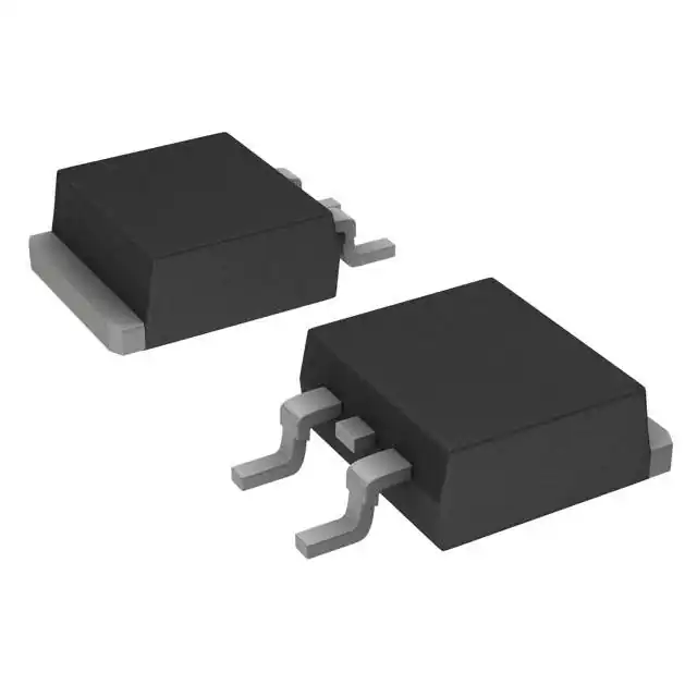
D2Pak
IRF3610SPbF
G
D
S
Gate
Drain
Source
Absolute Maximum Ratings
Symbol
Parameter
ID @ TC = 25°C
ID @ TC = 100°C
IDM
PD @TC = 25°C
VGS
Max.
Continuous Drain Current, VGS @ 10V
Continuous Drain Current, VGS @ 10V
d
Pulsed Drain Current
Maximum Power Dissipation
Linear Derating Factor
Gate-to-Source Voltage
Peak Diode Recovery
Operating Junction and
Storage Temperature Range
Soldering Temperature, for 10 seconds
f
dv/dt
TJ
TSTG
Thermal Resistance
Symbol
RθJC
RθJA
1
c
Parameter
jk
Junction-to-Case
Junction-to-Ambient (PCB Mount)
i
www.irf.com © 2014 International Rectifier
W
W/°C
V
V/ns
°C
Single Pulse Avalanche Energy (Thermally Limited)
Avalanche Current
Repetitive Avalanche Energy
�c
A
300 (1.6mm from case)
Avalanche Characteristics
EAS
IAR
EAR
Units
103
73
410
333
2.2
± 20
23
-55 to + 175
d
460
See Fig. 14, 15, 22a, 22b
mJ
A
mJ
Typ.
Max.
Units
–––
–––
0.50
40
°C/W
Submit Datasheet Feedback
March 26, 2014
�IRF3610SPbF
Static @ TJ = 25°C (unless otherwise specified)
Symbol
Parameter
V(BR)DSS
∆V(BR)DSS/∆TJ
RDS(on)
VGS(th)
gfs
RG
IDSS
Drain-to-Source Breakdown Voltage
Breakdown Voltage Temp. Coefficient
Static Drain-to-Source On-Resistance
Gate Threshold Voltage
Forward Transconductance
Internal Gate Resistance
Drain-to-Source Leakage Current
IGSS
Gate-to-Source Forward Leakage
Gate-to-Source Reverse Leakage
Min. Typ. Max. Units
100
–––
–––
2.0
110
–––
–––
–––
–––
–––
–––
0.10
9.3
–––
–––
2.2
–––
–––
–––
–––
–––
–––
11.6
4.0
–––
–––
20
250
200
-200
Conditions
V VGS = 0V, ID = 250µA
V/°C Reference to 25°C, ID = 1.0mA
mΩ VGS = 10V, ID = 62A
V VDS = VGS, ID = 250µA
S VDS = 25V, ID = 62A
Ω
µA VDS = 100V, VGS = 0V
VDS = 100V, VGS = 0V, TJ = 125°C
nA VGS = 20V
VGS = -20V
c
f
Dynamic @ TJ = 25°C (unless otherwise specified)
Symbol
Qg
Qgs
Qgd
Qsync
td(on)
tr
td(off)
tf
Ciss
Coss
Crss
Coss eff. (ER)
Coss eff. (TR)
Parameter
Total Gate Charge
Gate-to-Source Charge
Gate-to-Drain ("Miller") Charge
Total Gate Charge Sync. (Qg - Qgd)
Turn-On Delay Time
Rise Time
Turn-Off Delay Time
Fall Time
Input Capacitance
Output Capacitance
Reverse Transfer Capacitance
Effective Output Capacitance (Energy Related)
Effective Output Capacitance (Time Related)
Min. Typ. Max. Units
–––
–––
–––
–––
–––
–––
–––
–––
–––
–––
–––
–––
–––
100
23
42
58
15
55
77
43
5380
690
100
560
750
150
–––
–––
–––
–––
–––
–––
–––
–––
–––
–––
–––
–––
nC
Conditions
ID = 62A
VDS =50V
VGS = 10V
ID = 62A, VDS =0V, VGS = 10V
VDD = 65V
ID = 62A
RG = 2.7Ω
VGS = 10V
VGS = 0V
VDS = 25V
ƒ = 1.0 MHz, See Fig. 5
VGS = 0V, VDS = 0V to 80V , See Fig. 11
VGS = 0V, VDS = 0V to 80V
f
ns
pF
f
h
g
Diode Characteristics
Symbol
IS
Parameter
Continuous Source Current
VSD
trr
(Body Diode)
Pulsed Source Current
(Body Diode)
Diode Forward Voltage
Reverse Recovery Time
Qrr
Reverse Recovery Charge
IRRM
ton
Reverse Recovery Current
Forward Turn-On Time
ISM
�d
Notes:
Repetitive rating; pulse width limited by max. junction
temperature.
Limited by TJmax, starting TJ = 25°C, L = 0.24mH
RG = 50Ω, IAS = 62A, VGS =10V. Part not recommended for use
above this value.
ISD ≤ 62A, di/dt ≤ 1935A/µs, VDD ≤ V(BR)DSS, TJ ≤ 175°C.
Pulse width ≤ 400µs; duty cycle ≤ 2%.
Coss eff. (TR) is a fixed capacitance that gives the same charging
time as Coss while VDS is rising from 0 to 80% VDSS .
2
www.irf.com © 2014 International Rectifier
Min. Typ. Max. Units
–––
–––
–––
–––
103
410
Conditions
A
MOSFET symbol
A
showing the
integral reverse
D
G
p-n junction diode.
TJ = 25°C, IS = 62A, VGS = 0V
VR = 85V,
TJ = 25°C
TJ = 125°C
IF = 62A
di/dt = 100A/µs
TJ = 25°C
S
f
––– –––
1.3
V
––– 110 –––
ns
––– 120 –––
––– 570 –––
nC
TJ = 125°C
––– 710 –––
––– -9.5 –––
A TJ = 25°C
Intrinsic turn-on time is negligible (turn-on is dominated by LS+LD)
f
Coss eff. (ER) is a fixed capacitance that gives the same energy as
Coss while VDS is rising from 0 to 80% VDSS.
When mounted on 1" square PCB (FR-4 or G-10 Material). For recom-
mended footprint and soldering techniques refer to application note #AN-994.
Rθ is measured at TJ approximately 90°C.
RθJC value shown is at time zero.
Submit Datasheet Feedback
March 26, 2014
�IRF3610SPbF
1000
1000
100
BOTTOM
100
10
1
VGS
15V
10V
6.0V
5.0V
4.7V
4.5V
4.2V
4.0V
TOP
ID, Drain-to-Source Current (A)
ID, Drain-to-Source Current (A)
TOP
VGS
15V
10V
6.0V
5.0V
4.7V
4.5V
4.2V
4.0V
4.0V
BOTTOM
4.0V
10
≤60µs PULSE WIDTH
≤60µs PULSE WIDTH
Tj = 175°C
Tj = 25°C
1
0.1
0.1
1
10
100
0.1
1000
Fig 1. Typical Output Characteristics
3.0
RDS(on) , Drain-to-Source On Resistance
(Normalized)
ID, Drain-to-Source Current (A)
100
Fig 2. Typical Output Characteristics
1000
T J = 175°C
100
TJ = 25°C
10
1
VDS = 50V
≤60µs PULSE WIDTH
0.1
ID = 62A
VGS = 10V
2.5
2.0
1.5
1.0
0.5
2
3
4
5
6
7
8
9
10
11
-60 -40 -20 0 20 40 60 80 100120140160180
T J , Junction Temperature (°C)
VGS, Gate-to-Source Voltage (V)
Fig 4. Normalized On-Resistance vs. Temperature
Fig 3. Typical Transfer Characteristics
100000
14.0
VGS = 0V,
f = 1 MHZ
C iss = C gs + C gd, C ds SHORTED
C rss = C gd
VGS, Gate-to-Source Voltage (V)
ID= 62A
C oss = C ds + C gd
10000
C, Capacitance (pF)
10
V DS, Drain-to-Source Voltage (V)
V DS, Drain-to-Source Voltage (V)
Ciss
Coss
1000
Crss
100
12.0
VDS= 80V
VDS= 50V
VDS= 20V
10.0
8.0
6.0
4.0
2.0
0.0
10
1
10
100
VDS, Drain-to-Source Voltage (V)
Fig 5. Typical Capacitance vs. Drain-to-Source Voltage
3
1
www.irf.com © 2014 International Rectifier
0
20
40
60
80
100
120
140
QG, Total Gate Charge (nC)
Fig 6. Typical Gate Charge vs. Gate-to-Source Voltage
Submit Datasheet Feedback
March 26, 2014
�IRF3610SPbF
10000
1000
ID, Drain-to-Source Current (A)
ISD, Reverse Drain Current (A)
OPERATION IN THIS AREA
LIMITED BY R DS(on)
T J = 175°C
100
T J = 25°C
10
1000
100
100µs
10
1ms
1
VGS = 0V
1.0
10ms
DC
0.1
0.0
0.5
1.0
1.5
2.0
1
VSD, Source-to-Drain Voltage (V)
80
60
40
20
0
75
100
125
150
175
V(BR)DSS , Drain-to-Source Breakdown Voltage (V)
100
50
100
125
ID = 1.0mA
120
115
110
105
100
95
-60 -40 -20 0 20 40 60 80 100120140160180
T J , Temperature ( °C )
T C , Case Temperature (°C)
Fig 9. Maximum Drain Current vs.
Case Temperature
Fig 10. Drain-to-Source Breakdown Voltage
3.5
EAS , Single Pulse Avalanche Energy (mJ)
2000
3.0
ID
13A
27A
BOTTOM 62A
TOP
1600
Energy (µJ)
2.5
1200
2.0
1.5
1.0
0.5
0.0
800
400
0
0
20
40
60
80
100
120
VDS, Drain-to-Source Voltage (V)
Fig 11. Typical COSS Stored Energy
4
1000
Fig 8. Maximum Safe Operating Area
120
25
10
VDS , Drain-toSource Voltage (V)
Fig 7. Typical Source-Drain Diode
Forward Voltage
ID, Drain Current (A)
3ms
Tc = 25°C
Tj = 175°C
Single Pulse
www.irf.com © 2014 International Rectifier
25
50
75
100
125
150
175
Starting T J , Junction Temperature (°C)
Fig 12. Maximum Avalanche Energy vs. DrainCurrent
Submit Datasheet Feedback
March 26, 2014
�IRF3610SPbF
Thermal Response ( Z thJC ) °C/W
1
D = 0.50
0.20
0.1
0.10
0.05
0.01
0.02
0.01
0.001
SINGLE PULSE
( THERMAL RESPONSE )
0.0001
1E-006
1E-005
Notes:
1. Duty Factor D = t1/t2
2. Peak Tj = P dm x Zthjc + Tc
0.0001
0.001
0.01
0.1
1
t1 , Rectangular Pulse Duration (sec)
Fig 13. Maximum Effective Transient Thermal Impedance Junction-to-Case
Avalanche Current (A)
1000
Allowed avalanche Current vs avalanche
pulsewidth, tav, assuming ∆Tj = 150°C and
Tstart =25°C (Single Pulse)
100
10
1
Allowed avalanche Current vs avalanche
pulsewidth, tav, assuming ∆Τj = 25°C and
Tstart = 150°C.
0.1
1.0E-06
1.0E-05
1.0E-04
1.0E-03
1.0E-02
1.0E-01
tav (sec)
Fig 14. Typical Avalanche Current vs. Pulse Width
EAR , Avalanche Energy (mJ)
500
Notes on Repetitive Avalanche Curves , Figures 14, 15:
(For further info, see AN-1005 at www.irf.com)
1. Avalanche failures assumption:
Purely a thermal phenomenon and failure occurs at a temperature far in
excess of Tjmax. This is validated for every part type.
2. Safe operation in Avalanche is allowed as long asTjmax is not exceeded.
3. Equation below based on circuit and waveforms shown in Figures 16a, 16b.
4. PD (ave) = Average power dissipation per single avalanche pulse.
5. BV = Rated breakdown voltage (1.3 factor accounts for voltage increase
during avalanche).
6. Iav = Allowable avalanche current.
7. ∆T = Allowable rise in junction temperature, not to exceed Tjmax (assumed as
25°C in Figure 13, 15).
tav = Average time in avalanche.
D = Duty cycle in avalanche = tav ·f
ZthJC(D, tav) = Transient thermal resistance, see Figures 13)
TOP
Single Pulse
BOTTOM 1.0% Duty Cycle
ID = 62A
400
300
200
100
0
25
50
75
100
125
150
175
Starting T J , Junction Temperature (°C)
PD (ave) = 1/2 ( 1.3·BV·Iav) = DT/ ZthJC
Iav = 2DT/ [1.3·BV·Zth]
EAS (AR) = PD (ave)·tav
Fig 15. Maximum Avalanche Energy vs. Temperature
5
www.irf.com © 2014 International Rectifier
Submit Datasheet Feedback
March 26, 2014
�IRF3610SPbF
60
4.0
3.5
IRRM (A)
VGS(th) , Gate threshold Voltage (V)
4.5
3.0
ID = 250µA
2.5
50
IF = 41A
V R = 85V
40
TJ = 25°C
TJ = 125°C
30
20
ID = 1.0mA
ID = 1.0A
10
2.0
1.5
-100
0
-50
0
50
100
150
100 200 300 400 500 600 700 800 900 1000
200
diF /dt (A/µs)
T J , Temperature ( °C )
Fig. 17 - Typical Recovery Current vs. dif/dt
Fig 16. Threshold Voltage vs. Temperature
4000
50
IF = 62A
V R = 85V
40
TJ = 25°C
TJ = 125°C
3500
3000
QRR (nC)
IRRM (A)
60
30
20
IF = 41A
V R = 85V
TJ = 25°C
TJ = 125°C
2500
2000
1500
10
1000
500
0
100 200 300 400 500 600 700 800 900 1000
100 200 300 400 500 600 700 800 900 1000
diF /dt (A/µs)
diF /dt (A/µs)
Fig. 19 - Typical Stored Charge vs. dif/dt
Fig. 18 - Typical Recovery Current vs. dif/dt
4000
3500
QRR (nC)
3000
IF = 62A
V R = 85V
TJ = 25°C
TJ = 125°C
2500
2000
1500
1000
500
100 200 300 400 500 600 700 800 900 1000
diF /dt (A/µs)
Fig. 20 - Typical Stored Charge vs. dif/dt
6
www.irf.com © 2014 International Rectifier
Submit Datasheet Feedback
March 26, 2014
�IRF3610SPbF
Driver Gate Drive
D.U.T
-
-
-
*
D.U.T. ISD Waveform
Reverse
Recovery
Current
+
RG
•
•
•
•
dv/dt controlled by RG
Driver same type as D.U.T.
I SD controlled by Duty Factor "D"
D.U.T. - Device Under Test
VDD
P.W.
Period
VGS=10V
Circuit Layout Considerations
• Low Stray Inductance
• Ground Plane
• Low Leakage Inductance
Current Transformer
+
D=
Period
P.W.
+
+
-
Body Diode Forward
Current
di/dt
D.U.T. VDS Waveform
Diode Recovery
dv/dt
Re-Applied
Voltage
Body Diode
VDD
Forward Drop
Inductor
Current
Inductor Curent
ISD
Ripple ≤ 5%
* VGS = 5V for Logic Level Devices
Fig 21. Peak Diode Recovery dv/dt Test Circuit for N-Channel
HEXFET® Power MOSFETs
V(BR)DSS
15V
DRIVER
L
VDS
tp
D.U.T
RG
VGS
20V
+
V
- DD
IAS
A
0.01Ω
tp
I AS
Fig 22a. Unclamped Inductive Test Circuit
RD
VDS
Fig 22b. Unclamped Inductive Waveforms
VDS
90%
VGS
D.U.T.
RG
+
- VDD
V10V
GS
10%
VGS
Pulse Width ≤ 1 µs
Duty Factor ≤ 0.1 %
td(on)
Fig 23a. Switching Time Test Circuit
tr
t d(off)
Fig 23b. Switching Time Waveforms
Id
Current Regulator
Same Type as D.U.T.
Vds
Vgs
50KΩ
12V
tf
.2µF
.3µF
D.U.T.
+
V
- DS
Vgs(th)
VGS
3mA
IG
ID
Current Sampling Resistors
Fig 24a. Gate Charge Test Circuit
7
www.irf.com © 2014 International Rectifier
Qgs1 Qgs2
Qgd
Qgodr
Fig 24b. Gate Charge Waveform
Submit Datasheet Feedback
March 26, 2014
�IRF3610SPbF
D2Pak (TO-263AB) Package Outline
Dimensions are shown in millimeters (inches)
D2Pak (TO-263AB) Part Marking Information
Note: For the most current drawing please refer to IR website at http://www.irf.com/package/
8
www.irf.com © 2014 International Rectifier
Submit Datasheet Feedback
March 26, 2014
�IRF3610SPbF
D2Pak (TO-263AB) Tape & Reel Information
Dimensions are shown in millimeters (inches)
TRR
1.60 (.063)
1.50 (.059)
4.10 (.161)
3.90 (.153)
FEED DIRECTION 1.85 (.073)
1.65 (.065)
1.60 (.063)
1.50 (.059)
11.60 (.457)
11.40 (.449)
0.368 (.0145)
0.342 (.0135)
15.42 (.609)
15.22 (.601)
24.30 (.957)
23.90 (.941)
TRL
10.90 (.429)
10.70 (.421)
1.75 (.069)
1.25 (.049)
4.72 (.136)
4.52 (.178)
16.10 (.634)
15.90 (.626)
FEED DIRECTION
13.50 (.532)
12.80 (.504)
27.40 (1.079)
23.90 (.941)
4
330.00
(14.173)
MAX.
60.00 (2.362)
MIN.
NOTES :
1. COMFORMS TO EIA-418.
2. CONTROLLING DIMENSION: MILLIMETER.
3. DIMENSION MEASURED @ HUB.
4. INCLUDES FLANGE DISTORTION @ OUTER EDGE.
26.40 (1.039)
24.40 (.961)
3
30.40 (1.197)
MAX.
4
Note: For the most current drawing please refer to IR website at http://www.irf.com/package/
IR WORLD HEADQUARTERS: 101 N. Sepulveda Blvd., El Segundo, California 90245, USA
To contact International Rectifier, please visit http://www.irf.com/whoto-call/
9
www.irf.com © 2014 International Rectifier
Submit Datasheet Feedback
March 26, 2014
�IMPORTANT NOTICE
The information given in this document shall in no
event be regarded as a guarantee of conditions or
characteristics (“Beschaffenheitsgarantie”) .
With respect to any examples, hints or any typical
values stated herein and/or any information
regarding the application of the product, Infineon
Technologies hereby disclaims any and all
warranties and liabilities of any kind, including
without limitation warranties of non-infringement
of intellectual property rights of any third party.
In addition, any information given in this document
is subject to customer’s compliance with its
obligations stated in this document and any
applicable legal requirements, norms and
standards concerning customer’s products and any
use of the product of Infineon Technologies in
customer’s applications.
The data contained in this document is exclusively
intended for technically trained staff. It is the
responsibility of customer’s technical departments
to evaluate the suitability of the product for the
intended application and the completeness of the
product information given in this document with
respect to such application.
For further information on the product, technology,
delivery terms and conditions and prices please
contact your nearest Infineon Technologies office
(www.infineon.com).
WARNINGS
Due to technical requirements products may
contain dangerous substances. For information on
the types in question please contact your nearest
Infineon Technologies office.
Except as otherwise explicitly approved by Infineon
Technologies in a written document signed by
authorized
representatives
of
Infineon
Technologies, Infineon Technologies’ products may
not be used in any applications where a failure of
the product or any consequences of the use thereof
can reasonably be expected to result in personal
injury.
�