PD - 95385
SMPS MOSFET
Applications
High Frequency DC-DC Isolated
Converters with Synchronous Rectification
for Telecom and Industrial Use
l High Frequency Buck Converters for
Computer Processor Power
l Lead-Free
IRF3706PbF
IRF3706SPbF
IRF3706LPbF
HEXFET® Power MOSFET
l
VDSS
RDS(on) max
ID
20V
8.5mΩ
77A
Benefits
l
Ultra-Low Gate Impedance
l
Very Low RDS(on) at 4.5V VGS
l
Fully Characterized Avalanche Voltage
and Current
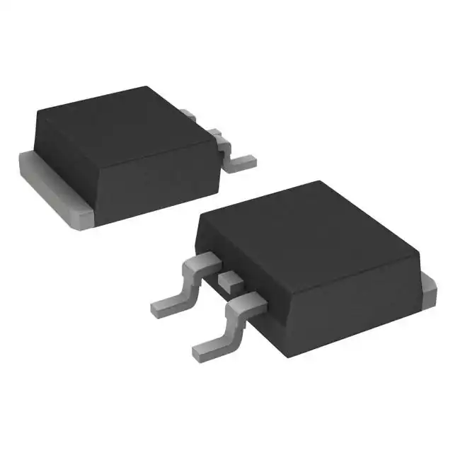
TO-220AB
IRF3706
D2Pak
IRF3706S
TO-262
IRF3706L
Notes through are on page 11
www.irf.com
1
06/08/04
�IRF3706/S/LPbF
2
www.irf.com
�IRF3706/S/LPbF
Fig 1. Typical Output Characteristics
Fig 3. Typical Transfer Characteristics
www.irf.com
Fig 2. Typical Output Characteristics
Fig 4. Normalized On-Resistance
Vs. Temperature
3
�IRF3706/S/LPbF
4
Fig 5. Typical Capacitance Vs.
Drain-to-Source Voltage
Fig 6. Typical Gate Charge Vs.
Gate-to-Source Voltage
Fig 7. Typical Source-Drain Diode
Forward Voltage
Fig 8. Maximum Safe Operating Area
www.irf.com
�IRF3706/S/LPbF
V DS
VGS
RG
RD
D.U.T.
+
- VDD
10V
Pulse Width ≤ 1 µs
Duty Factor ≤ 0.1 %
Fig 10a. Switching Time Test Circuit
VDS
90%
10%
VGS
Fig 9. Maximum Drain Current Vs.
Case Temperature
td(on)
tr
t d(off)
tf
Fig 10b. Switching Time Waveforms
Fig 11. Maximum Effective Transient Thermal Impedance, Junction-to-Case
www.irf.com
5
�IRF3706/S/LPbF
15V
L
VDS
D.U.T
RG
IAS
VGS
20V
DRIVER
+
V
- DD
A
0.01Ω
tp
Fig 12a. Unclamped Inductive Test Circuit
V(BR)DSS
tp
Fig 12c. Maximum Avalanche Energy
Vs. Drain Current
I AS
Fig 12b. Unclamped Inductive Waveforms
Current Regulator
Same Type as D.U.T.
50KΩ
QG
12V
.2µF
.3µF
VGS
QGS
D.U.T.
QGD
+
V
- DS
VGS
VG
3mA
IG
Charge
Fig 13a. Basic Gate Charge Waveform
6
ID
Current Sampling Resistors
Fig 13b. Gate Charge Test Circuit
www.irf.com
�IRF3706/S/LPbF
Peak Diode Recovery dv/dt Test Circuit
+
D.U.T*
Circuit Layout Considerations
• Low Stray Inductance
• Ground Plane
• Low Leakage Inductance
Current Transformer
+
-
-
+
RG
• dv/dt controlled by RG
• ISD controlled by Duty Factor "D"
• D.U.T. - Device Under Test
V GS
*
+
-
V DD
Reverse Polarity of D.U.T for P-Channel
Driver Gate Drive
P.W.
Period
D=
P.W.
Period
[VGS=10V ] ***
D.U.T. ISD Waveform
Reverse
Recovery
Current
Body Diode Forward
Current
di/dt
D.U.T. VDS Waveform
Diode Recovery
dv/dt
Re-Applied
Voltage
Body Diode
[VDD]
Forward Drop
Inductor Curent
Ripple ≤ 5%
[ISD]
*** VGS = 5.0V for Logic Level and 3V Drive Devices
Fig 14. For N-channel HEXFET® power MOSFETs
www.irf.com
7
�IRF3706/S/LPbF
TO-220AB Package Outline
Dimensions are shown in millimeters (inches)
2.87 (.113)
2.62 (.103)
10.54 (.415)
10.29 (.405)
-B-
3.78 (.149)
3.54 (.139)
4.69 (.185)
4.20 (.165)
-A-
1.32 (.052)
1.22 (.048)
6.47 (.255)
6.10 (.240)
4
15.24 (.600)
14.84 (.584)
LEAD ASSIGNMENTS
1.15 (.045)
MIN
1
2
3
14.09 (.555)
13.47 (.530)
1.40 (.055)
1.15 (.045)
IGBTs, CoPACK
2 - DRAIN
1- GATE
3 - SOURCE
2- DRAIN
3- SOURCE
4 - DRAIN
4- DRAIN
1234-
GATE
COLLECTOR
EMITTER
COLLECTOR
4.06 (.160)
3.55 (.140)
3X
3X
LEAD ASSIGNMENTS
HEXFET
1 - GATE
0.93 (.037)
0.69 (.027)
0.36 (.014)
3X
M
B A M
0.55 (.022)
0.46 (.018)
2.92 (.115)
2.64 (.104)
2.54 (.100)
2X
NOTES:
1 DIMENSIONING & TOLERANCING PER ANSI Y14.5M, 1982.
2 CONTROLLING DIMENSION : INCH
3 OUTLINE CONFORMS TO JEDEC OUTLINE TO-220AB.
4 HEATSINK & LEAD MEASUREMENTS DO NOT INCLUDE BURRS.
TO-220AB Part Marking Information
E XAMPL E : T H IS IS AN IR F 1010
L OT CODE 1789
AS S E MB L E D ON WW 19, 1997
IN T H E AS S E MB L Y L INE "C"
Note: "P" in assembly line
position indicates "Lead-Free"
INT E R NAT IONAL
R E CT IF IE R
L OGO
AS S E MB L Y
L OT CODE
8
PAR T NU MB E R
DAT E CODE
YE AR 7 = 1997
WE E K 19
L INE C
www.irf.com
�IRF3706/S/LPbF
D2Pak Package Outline
Dimensions are shown in millimeters (inches)
D2Pak Part Marking Information
T HIS IS AN IRF 530S WIT H
LOT CODE 8024
AS S E MB LE D ON WW 02, 2000
IN T HE AS S E MB LY LINE "L"
INT E RNAT IONAL
RE CT IF IE R
LOGO
Note: "P" in as s embly line
pos ition indicates "Lead-F ree"
PART NUMB E R
F 530S
AS SE MB LY
LOT CODE
DAT E CODE
YEAR 0 = 2000
WE EK 02
LINE L
OR
INT ERNATIONAL
RE CT IFIE R
LOGO
AS S EMBLY
LOT CODE
www.irf.com
PART NUMBER
F530S
DAT E CODE
P = DES IGNAT ES LEAD-FR EE
PRODUCT (OPTIONAL)
YEAR 0 = 2000
WEE K 02
A = AS S EMBLY S IT E CODE
9
�IRF3706/S/LPbF
TO-262 Package Outline
Dimensions are shown in millimeters (inches)
TO-262 Part Marking Information
EXAMPLE: T HIS IS AN IR L3103L
L OT CODE 1789
AS S E MBLED ON WW 19, 1997
IN T HE AS S EMB LY LINE "C"
Note: "P" in ass embly line
pos ition indicates "Lead-Free"
INT ERNAT IONAL
R ECT IFIER
LOGO
AS S EMBLY
LOT CODE
PART NUMBER
DAT E CODE
YEAR 7 = 1997
WEEK 19
LINE C
OR
INT ERNAT IONAL
RECT IFIER
LOGO
AS S EMBLY
L OT CODE
10
PART NUMBER
DAT E CODE
P = DES IGNAT ES LEAD-F REE
PRODUCT (OPT IONAL)
YE AR 7 = 1997
WEE K 19
A = AS S EMBL Y S IT E CODE
www.irf.com
�IRF3706/S/LPbF
D2Pak Tape & Reel Information
Dimensions are shown in millimeters (inches)
TRR
1.60 (.063)
1.50 (.059)
4.10 (.161)
3.90 (.153)
FEED DIRECTION
1.85 (.073)
1.65 (.065)
1.60 (.063)
1.50 (.059)
11.60 (.457)
11.40 (.449)
0.368 (.0145)
0.342 (.0135)
15.42 (.609)
15.22 (.601)
24.30 (.957)
23.90 (.941)
TRL
10.90 (.429)
10.70 (.421)
1.75 (.069)
1.25 (.049)
4.72 (.136)
4.52 (.178)
16.10 (.634)
15.90 (.626)
FEED DIRECTION
13.50 (.532)
12.80 (.504)
27.40 (1.079)
23.90 (.941)
4
330.00
(14.173)
MAX.
NOTES :
1. COMFORMS TO EIA-418.
2. CONTROLLING DIMENSION: MILLIMETER.
3. DIMENSION MEASURED @ HUB.
4. INCLUDES FLANGE DISTORTION @ OUTER EDGE.
Notes:
Repetitive rating; pulse width limited by
max. junction temperature.
Starting TJ = 25°C, L = 0.54mH, RG = 25Ω,
IAS = 28A.
Pulse width ≤ 400µs; duty cycle ≤ 2%.
60.00 (2.362)
MIN.
26.40 (1.039)
24.40 (.961)
3
30.40 (1.197)
MAX.
4
This is only applied to TO-220AB pakcage.
This is applied to D2Pak, when mounted on 1" square PCB (FR4 or G-10 Material). For recommended footprint and soldering
techniques refer to application note #AN-994.
Calculated continuous current based on maximum allowable
junction temperature. Package limitation current is 75A.
Data and specifications subject to change without notice.
IR WORLD HEADQUARTERS: 233 Kansas St., El Segundo, California 90245, USA Tel: (310) 252-7105
TAC Fax: (310) 252-7903
Visit us at www.irf.com for sales contact information. 06/04
www.irf.com
11
�Note: For the most current drawings please refer to the IR website at:
http://www.irf.com/package/
�
很抱歉,暂时无法提供与“IRF3706SPBF”相匹配的价格&库存,您可以联系我们找货
免费人工找货