IRF5801PbF-1
HEXFET® Power MOSFET
VDS
RDS(on) max
(@VGS = 10V)
Qg (typical)
ID
(@TA = 25°C)
200
V
2.20
Ω
3.9
0.6
D
1
6
D
nC
D
2
5
D
A
G
3
4
S
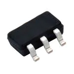
TSOP-6
Features
Industry-standard pinout TSOP-6 Package
Compatible with Existing Surface Mount Techniques
RoHS Compliant, Halogen-Free
MSL1, Industrial qualification
Base Part Number
Package Type
IRF5801TRPbF-1
TSOP-6
⇒
Benefits
Multi-Vendor Compatibility
Easier Manufacturing
Environmentally Friendlier
Increased Reliability
Standard Pack
Form
Quantity
Tape and Reel
3000
Orderable Part Number
IRF5801TRPbF-1
Absolute Maximum Ratings
Parameter
ID @ TA = 25°C
ID @ TA = 70°C
IDM
PD @TA = 25°C
VGS
dv/dt
TJ
TSTG
Continuous Drain Current, VGS @ 10V
Continuous Drain Current, VGS @ 10V
Pulsed Drain Current
Power Dissipation
Linear Derating Factor
Gate-to-Source Voltage
Peak Diode Recovery dv/dt
Operating Junction and
Storage Temperature Range
Soldering Temperature, for 10 seconds
Max.
Units
0.6
0.48
4.8
2.0
0.016
± 30
9.6
-55 to + 150
A
W
W/°C
V
V/ns
°C
300 (1.6mm from case )
Thermal Resistance
Symbol
RθJA
Parameter
Junction-to-Ambient
Typ.
Max.
Units
–––
62.5
°C/W
Notes through are on page 8
1
www.irf.com © 2014 International Rectifier
Submit Datasheet Feedback
July 15, 2014
�IRF5801PbF-1
Static @ TJ = 25°C (unless otherwise specified)
Parameter
Drain-to-Source Breakdown Voltage
ΔV(BR)DSS/ΔTJ Breakdown Voltage Temp. Coefficient
RDS(on)
Static Drain-to-Source On-Resistance
VGS(th)
Gate Threshold Voltage
V(BR)DSS
IDSS
Drain-to-Source Leakage Current
IGSS
Gate-to-Source Forward Leakage
Gate-to-Source Reverse Leakage
Min.
200
–––
–––
3.0
–––
–––
–––
–––
Typ.
–––
0.26
–––
–––
–––
–––
–––
–––
Max. Units
Conditions
–––
V
VGS = 0V, ID = 250μA
––– V/°C Reference to 25°C, ID = 1mA
2.2
Ω
VGS = 10V, ID = 0.36A
5.5
V
VDS = VGS, ID = 250μA
25
VDS = 200V, VGS = 0V
μA
250
VDS = 160V, VGS = 0V, TJ = 150°C
100
VGS = 30V
nA
-100
VGS = -30V
Dynamic @ TJ = 25°C (unless otherwise specified)
gfs
Qg
Qgs
Qgd
td(on)
tr
td(off)
tf
Ciss
Coss
Crss
Coss
Coss
Coss eff.
Parameter
Forward Transconductance
Total Gate Charge
Gate-to-Source Charge
Gate-to-Drain ("Miller") Charge
Turn-On Delay Time
Rise Time
Turn-Off Delay Time
Fall Time
Input Capacitance
Output Capacitance
Reverse Transfer Capacitance
Output Capacitance
Output Capacitance
Effective Output Capacitance
Min. Typ. Max. Units
Conditions
0.44 ––– –––
S
VDS = 50V, ID = 0.36A
–––
3.9 –––
ID = 0.36A
–––
0.8 –––
nC
VDS = 160V
–––
2.2 –––
VGS = 10V
–––
6.5 –––
VDD = 100V
–––
8.0 –––
ID = 0.36A
ns
–––
8.8 –––
RG = 53Ω
–––
19 –––
VGS = 10V
–––
88 –––
VGS = 0V
–––
18 –––
VDS = 25V
–––
6.3 –––
pF
ƒ = 1.0MHz
––– 102 –––
VGS = 0V, VDS = 1.0V, ƒ = 1.0MHz
–––
8.4 –––
VGS = 0V, VDS = 160V, ƒ = 1.0MHz
–––
26 –––
VGS = 0V, VDS = 0V to 160V
Avalanche Characteristics
Parameter
EAS
IAR
Single Pulse Avalanche Energy
Avalanche Current
Typ.
Max.
Units
–––
–––
9.9
0.6
mJ
A
Diode Characteristics
IS
ISM
VSD
trr
Qrr
2
Parameter
Continuous Source Current
(Body Diode)
Pulsed Source Current
(Body Diode)
Diode Forward Voltage
Reverse Recovery Time
Reverse RecoveryCharge
www.irf.com © 2014 International Rectifier
Min. Typ. Max. Units
–––
–––
1.8
–––
–––
4.8
–––
–––
–––
–––
45
54
1.3
–––
–––
A
V
ns
nC
Conditions
MOSFET symbol
showing the
G
integral reverse
p-n junction diode.
TJ = 25°C, IS = 0.36A, VGS = 0V
TJ = 25°C, IF = 0.36A
di/dt = 100A/μs
Submit Datasheet Feedback
D
S
July 15, 2014
�IRF5801PbF-1
1
10
VGS
TOP
15.0V
12.0V
10.0V
8.0V
7.5V
7.0V
6.5V
BOTTOM 6.0V
VGS
15.0V
12.0V
10.0V
8.0V
7.5V
7.0V
6.5V
BOTTOM 6.0V
TOP
ID, Drain-to-Source Current (A)
ID, Drain-to-Source Current (A)
10
6.0V
0.1
1
6.0V
0.1
20μs PULSE WIDTH
Tj = 150°C
20μs PULSE WIDTH
Tj = 25°C
0.01
0.01
0.1
1
10
100
0.1
VDS, Drain-to-Source Voltage (V)
RDS(on) , Drain-to-Source On Resistance
(Normalized)
I D , Drain-to-Source Current (A)
TJ = 150° C
1
TJ = 25 ° C
V DS = 50V
20μs PULSE WIDTH
7
8
9
10
11
12
VGS , Gate-to-Source Voltage (V)
Fig 3. Typical Transfer Characteristics
3
100
Fig 2. Typical Output Characteristics
10
6
10
VDS, Drain-to-Source Voltage (V)
Fig 1. Typical Output Characteristics
0.1
1
www.irf.com © 2014 International Rectifier
3.0
ID = 0.6A
2.5
2.0
1.5
1.0
0.5
0.0
-60 -40 -20
VGS = 10V
0
20 40 60 80 100 120 140 160
TJ , Junction Temperature ( ° C)
Fig 4. Normalized On-Resistance
Vs. Temperature
Submit Datasheet Feedback
July 15, 2014
�IRF5801PbF-1
V GS = 0V, f = 1 MHZ
Ciss = Cgs + Cgd, Cds SHORTED
Crss = Cgd
C, Capacitance(pF)
120
Coss = Cds + Cgd
Ciss
80
Coss
40
Crss
20
VGS , Gate-to-Source Voltage (V)
160
10
100
V DS= 160V
V DS= 100V
V DS= 40V
16
12
8
4
0
1
ID = 0.36A
0
1000
0
1
2
3
4
5
QG , Total Gate Charge (nC)
VDS, Drain-to-Source Voltage (V)
Fig 6. Typical Gate Charge Vs.
Gate-to-Source Voltage
Fig 5. Typical Capacitance Vs.
Drain-to-Source Voltage
100
OPERATION IN THIS AREA LIMITED
BY RDS(on)
ID , Drain Current (A)
ISD , Reverse Drain Current (A)
10
TJ = 150 ° C
1
TJ = 25 ° C
0.1
0.4
4
V GS = 0 V
0.5
0.6
0.7
0.8
0.9
10
10us
1
1ms
0.1
0.01
1.0
100us
10ms
TC = 25 °C
TJ = 150 °C
Single Pulse
1
10
100
VSD ,Source-to-Drain Voltage (V)
VDS , Drain-to-Source Voltage (V)
Fig 7. Typical Source-Drain Diode
Forward Voltage
Fig 8. Maximum Safe Operating Area
www.irf.com © 2014 International Rectifier
Submit Datasheet Feedback
July 15, 2014
1000
�IRF5801PbF-1
0.6
VDS
VGS
ID , Drain Current (A)
0.5
RD
D.U.T.
RG
+
-V DD
0.4
10V
0.3
Pulse Width ≤ 1 µs
Duty Factor ≤ 0.1 %
0.2
Fig 10a. Switching Time Test Circuit
VDS
0.1
90%
0.0
25
50
75
100
125
TC , Case Temperature ( °C)
150
10%
VGS
Fig 9. Maximum Drain Current Vs.
Case Temperature
td(on)
tr
t d(off)
tf
Fig 10b. Switching Time Waveforms
Thermal Response(Z thJC )
100
D = 0.50
0.20
10
0.10
0.05
0.02
1
0.1
0.00001
PDM
0.01
t1
SINGLE PULSE
(THERMAL RESPONSE)
t2
Notes:
1. Duty factor D =t 1 / t 2
2. Peak TJ = P DM x Z thJC + TC
0.0001
0.001
0.01
0.1
1
10
t1 , Rectangular Pulse Duration (sec)
Fig 11. Maximum Effective Transient Thermal Impedance, Junction-to-Ambient
5
www.irf.com © 2014 International Rectifier
Submit Datasheet Feedback
July 15, 2014
100
�IRF5801PbF-1
2.500
(
RDS(on), Drain-to -Source On ResistanceΩ)
RDS ( on ) , Drain-to-Source On Resistance Ω
( )
12.000
10.000
2.250
8.000
VGS = 10V
2.000
6.000
4.000
ID = 0.6A
1.750
2.000
1.500
0.000
0
1
2
3
4
6.0
5
7.0
8.0
9.0
10.0 11.0 12.0 13.0 14.0 15.0
VGS, Gate -to -Source Voltage (V)
ID , Drain Current ( A )
Fig 12. On-Resistance Vs. Drain Current
Fig 13. On-Resistance Vs. Gate Voltage
Current Regulator
Same Type as D.U.T.
QG
VGS
QGS
.3μF
D.U.T.
+
V
- DS
QGD
EAS , Single Pulse Avalanche Energy (mJ)
50KΩ
.2μF
12V
VG
VGS
3mA
Charge
IG
ID
Current Sampling Resistors
Fig 14a&b. Basic Gate Charge Test Circuit
and Waveform
15V
V(BR)DSS
tp
L
VDS
DRIVER
D.U.T
RG
IAS
20V
I AS
tp
+
V
- DD
ID
0.4A
0.7A
BOTTOM 0.9A
TOP
20
15
10
5
0
25
50
75
100
125
www.irf.com © 2014 International Rectifier
150
Starting T J, Junction Temperature ( ° C)
0.01Ω
Fig 15a&b. Unclamped Inductive Test circuit
and Waveforms
6
A
25
Fig 15c. Maximum Avalanche Energy
Vs. Drain Current
Submit Datasheet Feedback
July 15, 2014
�IRF5801PbF-1
TSOP-6 Package Outline
TSOP-6 Part Marking Information
Y = YEAR
W = WEEK
PART NUMBER
YEAR
T OP
LOT
CODE
PART NUMBER CODE REFERENCE:
A = S I3443DV
B = IRF5800
C = IRF5850
D = IRF5851
E = IRF5852
F = IRF5801
G = IRF5803
H = IRF5804
I = IRF5805
J = IRF5806
K = IRF5810
N = IRF5802
DATE CODE MARKING INSTRUCTIONS
WW = (1-26) IF PRECEDED BY LAST DIGIT OF CALENDAR YEAR
O=
P=
R=
S=
IRLT S 6342T RPBF
IRFTS 8342T RPBF
IRFTS 9342T RPBF
Not applicable
T = IRLT S 2242T RPBF
Note: A line above the work week
(as s hown here) indicates Lead-Free.
2011
2012
2013
2014
2015
2016
2017
2018
2019
2020
2001
2002
2003
2004
2005
2006
2007
2008
2009
2010
Y
1
2
3
4
5
6
7
8
9
0
WORK
WEEK
W
01
02
03
04
A
B
C
D
24
25
26
X
Y
Z
WW = (27-52) IF PRECEDED BY A LETTER
YEAR
2011
2012
2013
2014
2015
2016
2017
2018
2019
2020
2001
2002
2003
2004
2005
2006
2007
2008
2009
2010
Y
A
B
C
D
E
F
G
H
J
K
WORK
WEEK
W
27
28
29
30
A
B
C
D
50
51
52
X
Y
Z
Note: For the most current drawing please refer to IR website at: http://www.irf.com/package/
7
www.irf.com © 2014 International Rectifier
Submit Datasheet Feedback
July 15, 2014
�IRF5801PbF-1
TSOP-6 Tape & Reel Information
8mm
FEED DIRECTION
4mm
NOTES :
1. OUTLINE CONFORMS TO EIA-481 & EIA-541.
178.00
( 7.008 )
MAX.
9.90 ( .390 )
8.40 ( .331 )
NOTES:
1. CONTROLLING DIMENSION : MILLIMETER.
2. OUTLINE CONFORMS TO EIA-481 & EIA-541.
Note: For the most current drawing please refer to IR website at: http://www.irf.com/package/
Notes:
Repetitive rating; pulse width limited by
max. junction temperature.
Starting TJ = 25°C, L = 27mH,
RG = 25Ω, IAS = 0.36A.
Pulse width ≤ 400μs; duty cycle ≤ 2%.
When mounted on 1 inch square copper board, t < 10sec.
Coss eff. is a fixed capacitance that gives the same charging
time as Coss while VDS is rising from 0 to 80% VDSS .
ISD ≤ 0.36A, di/dt ≤ 93A/μs, VDD ≤ V(BR)DSS, TJ ≤ 150°C.
†
Qualification information
Qualification level
Moisture Sensitivity Level
Industrial
(per JE DEC JE S D47F
TSOP-6
RoHS compliant
††
guidelines)
MS L1
††
(per JE DE C J-S TD-020D )
Yes
† Qualification standards can be found at International Rectifier’s web site: http://www.irf.com/product-info/reliability
†† Applicable version of JEDEC standard at the time of product release
IR WORLD HEADQUARTERS: 101 N. Sepulveda Blvd., El Segundo, California 90245, USA
To contact International Rectifier, please visit http://www.irf.com/whoto-call/
8
www.irf.com © 2014 International Rectifier
Submit Datasheet Feedback
July 15, 2014
�


 工商网监
湘ICP备2023018690号
工商网监
湘ICP备2023018690号
