IRF6216PbF-1
HEXFET® Power MOSFET
VDS
-150
RDS(on) max
(@VGS = -10V)
Qg (typical)
ID
(@TA = 25°C)
V
0.24
Ω
33
nC
-2.2
A
A
D
S
1
8
S
2
7
D
S
3
6
D
G
4
5
D
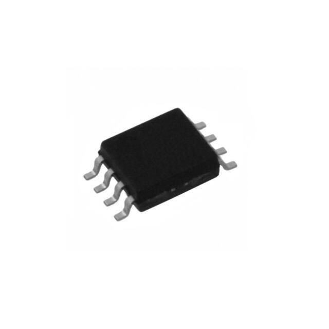
SO-8
Top View
Features
Benefits
Industry-standard pinout SO-8 Package
Compatible with Existing Surface Mount Techniques
RoHS Compliant, Halogen-Free
MSL1, Industrial qualification
Base Part Number
Package Type
IRF6216PbF-1
SO-8
Multi-Vendor Compatibility
Easier Manufacturing
Environmentally Friendlier
Increased Reliability
⇒
Standard Pack
Form
Quantity
Tube/Bulk
95
Tape and Reel
4000
Orderable Part Number
IRF6216PbF-1
IRF6216TRPbF-1
Absolute Maximum Ratings
Parameter
ID @ TA = 25°C
ID @ TA = 70°C
IDM
PD @TA = 25°C
VGS
dv/dt
TJ
TSTG
Continuous Drain Current, VGS @ 10V
Continuous Drain Current, VGS @ 10V
Pulsed Drain Current
Power Dissipation
Linear Derating Factor
Gate-to-Source Voltage
Peak Diode Recovery dv/dt
Operating Junction and
Storage Temperature Range
Soldering Temperature, for 10 seconds
Max.
Units
-2.2
-1.9
-19
2.5
0.02
± 20
7.8
-55 to + 150
A
W
W/°C
V
V/ns
°C
300 (1.6mm from case )
Thermal Resistance
Symbol
RθJL
RθJA
Parameter
Junction-to-Drain Lead
Junction-to-Ambient
Typ.
Max.
Units
–––
–––
20
50
°C/W
Notes through are on page 8
1
www.irf.com © 2014 International Rectifier
Submit Datasheet Feedback
June 30, 2014
�IRF6216PbF-1
Static @ TJ = 25°C (unless otherwise specified)
Parameter
Drain-to-Source Breakdown Voltage
ΔV(BR)DSS/ΔTJ Breakdown Voltage Temp. Coefficient
RDS(on)
Static Drain-to-Source On-Resistance
VGS(th)
Gate Threshold Voltage
V(BR)DSS
IDSS
Drain-to-Source Leakage Current
IGSS
Gate-to-Source Forward Leakage
Gate-to-Source Reverse Leakage
Min.
-150
–––
–––
-3.0
–––
–––
–––
–––
Typ.
–––
-0.17
–––
–––
–––
–––
–––
–––
Max. Units
Conditions
–––
V
VGS = 0V, ID = -250μA
––– V/°C Reference to 25°C, ID = -1mA
0.240
Ω
VGS = -10V, ID = -1.3A
-5.0
V
VDS = VGS, ID = -250μA
-25
VDS = -150V, VGS = 0V
μA
-250
VDS = -120V, VGS = 0V, TJ = 125°C
-100
VGS = -20V
nA
100
VGS = 20V
Dynamic @ TJ = 25°C (unless otherwise specified)
gfs
Qg
Qgs
Qgd
td(on)
tr
td(off)
tf
Ciss
Coss
Crss
Coss
Coss
Coss eff.
Parameter
Forward Transconductance
Total Gate Charge
Gate-to-Source Charge
Gate-to-Drain ("Miller") Charge
Turn-On Delay Time
Rise Time
Turn-Off Delay Time
Fall Time
Input Capacitance
Output Capacitance
Reverse Transfer Capacitance
Output Capacitance
Output Capacitance
Effective Output Capacitance
Min.
2.7
–––
–––
–––
–––
–––
–––
–––
–––
–––
–––
–––
–––
–––
Typ.
–––
33
7.2
15
18
15
33
26
1280
220
53
1290
99
220
Max. Units
Conditions
–––
S
VDS = -50V, ID = -1.3A
49
ID = -1.3A
11
nC
VDS = -120V
23
VGS = -10V,
–––
VDD = -75V
–––
ID = -1.3A
ns
–––
RG = 6.5Ω
–––
VGS = -10V
–––
VGS = 0V
–––
VDS = -25V
–––
pF
ƒ = 1.0MHz
–––
VGS = 0V, VDS = -1.0V, ƒ = 1.0MHz
–––
VGS = 0V, VDS = -120V, ƒ = 1.0MHz
–––
VGS = 0V, VDS = 0V to -120V
Avalanche Characteristics
Parameter
EAS
IAR
Single Pulse Avalanche Energy
Avalanche Current
Typ.
Max.
Units
–––
–––
200
-4.0
mJ
A
Diode Characteristics
IS
ISM
VSD
trr
Qrr
2
Parameter
Continuous Source Current
(Body Diode)
Pulsed Source Current
(Body Diode)
Diode Forward Voltage
Reverse Recovery Time
Reverse RecoveryCharge
www.irf.com © 2014 International Rectifier
Min. Typ. Max. Units
–––
–––
-2.2
–––
–––
-19
–––
–––
–––
–––
80
310
-1.6
120
460
A
V
nS
nC
Conditions
MOSFET symbol
showing the
G
integral reverse
p-n junction diode.
TJ = 25°C, IS = -1.3A, VGS = 0V
TJ = 25°C, IF = -1.3A
di/dt = -100A/μs
Submit Datasheet Feedback
D
S
June 30, 2014
�IRF6216PbF-1
TOP
-I D, Drain-to-Source Current (A)
10
BOTTOM
100
VGS
-15V
-12V
-10V
-8.0V
-7.0V
-6.0V
-5.5V
-5.0V
TOP
1
-I D, Drain-to-Source Current (A)
100
-5.0V
0.1
20μs PULSE WIDTH
T J= 25 ° C
0.01
0.1
1
10
BOTTOM
VGS
-15V
-12V
-10V
-8.0V
-7.0V
-6.0V
-5.5V
-5.0V
10
-5.0V
1
20μs PULSE WIDTH
T J= 150 ° C
0.1
0.1
100
1
10
100
-V DS, Drain-to-Source Voltage (V)
-V DS, Drain-to-Source Voltage (V)
Fig 1. Typical Output Characteristics
Fig 2. Typical Output Characteristics
100
2.5
I D = -2.2A
TJ = 150 ° C
1
V DS= -50V
20μs PULSE WIDTH
0.1
5.0
5.5
6.0
6.5
7.0
7.5
8.0
-V GS, Gate-to-Source Voltage (V)
Fig 3. Typical Transfer Characteristics
3
www.irf.com © 2014 International Rectifier
(Normalized)
10
RDS(on) , Drain-to-Source On Resistance
-I D, Drain-to-Source Current (A)
2.0
TJ = 25 ° C
1.5
1.0
0.5
V GS = -10V
0.0
-60
-40
-20
0
20
40
60
TJ , Junction Temperature
80
100
120
140
( ° C)
Fig 4. Normalized On-Resistance
Vs. Temperature
Submit Datasheet Feedback
June 30, 2014
160
�IRF6216PbF-1
10000
12
VGS = 0V,
f = 1 MHZ
Ciss = Cgs + Cgd, Cds SHORTED
Crss = Cgd
ID = -1.3A
VDS = -120V
VDS = -75V
VDS = -30V
10
Ciss
1000
-V GS , Gate-to-Source Voltage (V)
C, Capacitance(pF)
Coss = Cds + Cgd
Coss
100
Crss
10
8
6
4
2
0
1
10
100
0
1000
15
20
25
30
35
Fig 6. Typical Gate Charge Vs.
Gate-to-Source Voltage
Fig 5. Typical Capacitance Vs.
Drain-to-Source Voltage
100
-I D, Drain-to-Source Current (A)
100
-I SD, Reverse Drain Current (A)
10
QG , Total Gate Charge (nC)
-VDS, Drain-to-Source Voltage (V)
10
TJ = 150 ° C
TJ = 25 ° C
1
V GS= 0 V
0.1
0.4
0.6
0.8
1.0
-V SD,Source-to-Drain Voltage (V)
Fig 7. Typical Source-Drain Diode
Forward Voltage
4
5
www.irf.com © 2014 International Rectifier
OPERATION IN THIS AREA
LIMITED BY R DS(on)
10
100μsec
1msec
1
10msec
0.1
1.2
Tc = 25°C
Tj = 150°C
Single Pulse
1
10
100
1000
-VDS , Drain-toSource Voltage (V)
Fig 8. Maximum Safe Operating Area
Submit Datasheet Feedback
June 30, 2014
�IRF6216PbF-1
2.5
RD
V DS
VGS
2.0
D.U.T.
-I D , Drain Current (A)
RG
-
VDD
+
1.5
VGS
Pulse Width ≤ 1 µs
Duty Factor ≤ 0.1 %
1.0
Fig 10a. Switching Time Test Circuit
0.5
VDS
90%
0.0
25
50
75
100
125
150
TC , Case Temperature ( °C)
10%
VGS
Fig 9. Maximum Drain Current Vs.
Ambient Temperature
td(on)
tr
t d(off)
tf
Fig 10b. Switching Time Waveforms
(Z thJA )
100
D = 0.50
0.20
10
Thermal Response
0.10
0.05
P DM
0.02
1
t1
0.01
t2
SINGLE PULSE
(THERMAL RESPONSE)
Notes:
1. Duty factor D =
2. Peak T
0.1
0.0001
0.001
0.01
0.1
1
t1/ t 2
J = P DM x Z thJA
10
+T A
100
t 1, Rectangular Pulse Duration (sec)
Fig 11. Maximum Effective Transient Thermal Impedance, Junction-to-Ambient
5
www.irf.com © 2014 International Rectifier
Submit Datasheet Feedback
June 30, 2014
1000
�IRF6216PbF-1
R DS(on) , Drain-to -Source On Resistance (Ω)
R DS (on) , Drain-to-Source On Resistance ( Ω)
0.23
0.22
VGS = -10V
0.21
0.20
0.19
0
2
4
6
8
10
12
14
16
1.50
1.00
0.50
ID = -2.2A
0.00
4.5
18
6.0
7.5
9.0
10.5
12.0
13.5
15.0
-V GS, Gate -to -Source Voltage (V)
Fig 12. On-Resistance Vs. Drain Current
Fig 13. On-Resistance Vs. Gate Voltage
Current Regulator
Same Type as D.U.T.
QG
-VGS
50KΩ
.2μF
12V
QGS
.3μF
QGD
500
D.U.T.
+VDS
VG
TOP
VGS
400
IG
ID
Current Sampling Resistors
Fig 14a&b. Basic Gate Charge Test Circuit
and Waveform
L
VDS
I AS
D.U.T
RG
IAS
-20V
tp
VDD
A
DRIVER
0.01Ω
EAS , Single Pulse Avalanche Energy (mJ)
Charge
-3mA
BOTTOM
300
200
100
0
25
tp
V(BR)DSS
15V
Fig 15a&b. Unclamped Inductive Test circuit
and Waveforms
6
www.irf.com © 2014 International Rectifier
ID
-1.8A
-3.2A
-4.0A
50
75
100
Starting Tj, Junction Temperature
125
( ° C)
Fig 15c. Maximum Avalanche Energy
Vs. Drain Current
Submit Datasheet Feedback
June 30, 2014
150
�IRF6216PbF-1
SO-8 Package Outline(Mosfet & Fetky)
Dimensions are shown in milimeters (inches)
D
DIM
B
5
A
8
6
7
6
H
E
1
2
3
0.25 [.010]
4
A
MIN
.0532
.0688
1.35
1.75
A1 .0040
e
e1
8X b
0.25 [.010]
A
MAX
0.25
.0098
0.10
b
.013
.020
0.33
0.51
c
.0075
.0098
0.19
0.25
D
.189
.1968
4.80
5.00
E
.1497
.1574
3.80
4.00
e
.050 BAS IC
1.27 BASIC
.025 BAS IC
0.635 BAS IC
e1
6X
MILLIMETERS
MAX
A
5
INCHES
MIN
H
.2284
.2440
5.80
6.20
K
.0099
.0196
0.25
0.50
L
.016
.050
0.40
1.27
y
0°
8°
0°
8°
K x 45°
C
A1
y
0.10 [.004]
8X c
8X L
7
C A B
FOOT PRINT
NOT ES:
1. DIMENS IONING & T OLERANCING PER AS ME Y14.5M-1994.
2. CONT ROLLING DIMENSION: MILLIMET ER
8X 0.72 [.028]
3. DIMENS IONS ARE S HOWN IN MILLIMET ERS [INCHES ].
4. OUT LINE CONFORMS T O JEDEC OUT LINE MS-012AA.
5 DIMENS ION DOES NOT INCLUDE MOLD PROT RUS IONS .
MOLD PROT RUSIONS NOT T O EXCEED 0.15 [.006].
6 DIMENS ION DOES NOT INCLUDE MOLD PROT RUS IONS .
MOLD PROT RUSIONS NOT T O EXCEED 0.25 [.010].
6.46 [.255]
7 DIMENS ION IS T HE LENGT H OF LEAD FOR S OLDERING T O
A S UBS T RAT E.
3X 1.27 [.050]
8X 1.78 [.070]
SO-8 Part Marking Information
EXAMPLE: THIS IS AN IRF7101 (MOS FET )
INTERNATIONAL
RECT IFIER
LOGO
XXXX
F 7101
DAT E CODE (YWW)
P = DIS GNAT ES LEAD - FREE
PRODUCT (OPTIONAL)
Y = LAS T DIGIT OF T HE YEAR
WW = WEEK
A = AS S EMBLY SIT E CODE
LOT CODE
PART NUMBER
Note: For the most current drawing please refer to IR website at: http://www.irf.com/package/
7
www.irf.com © 2014 International Rectifier
Submit Datasheet Feedback
June 30, 2014
�IRF6216PbF-1
SO-8 Tape and Reel (Dimensions are shown in millimeters (inches))
TERMINAL NUMBER 1
12.3 ( .484 )
11.7 ( .461 )
8.1 ( .318 )
7.9 ( .312 )
FEED DIRECTION
NOTES:
1. CONTROLLING DIMENSION : MILLIMETER.
2. ALL DIMENSIONS ARE SHOWN IN MILLIMETERS(INCHES).
3. OUTLINE CONFORMS TO EIA-481 & EIA-541.
330.00
(12.992)
MAX.
14.40 ( .566 )
12.40 ( .488 )
NOTES :
1. CONTROLLING DIMENSION : MILLIMETER.
2. OUTLINE CONFORMS TO EIA-481 & EIA-541.
Note: For the most current drawing please refer to IR website at: http://www.irf.com/package/
Notes:
Repetitive rating; pulse width limited by max. junction temperature.
Starting TJ = 25°C, L = 25mH, RG = 25Ω, IAS = -4.0A.
Pulse width ≤ 400μs; duty cycle ≤ 2%.
When mounted on 1 inch square copper board.
†
Qualification information
Industrial
Qualification level
(per JEDE C JE S D47F
Moisture Sensitivity Level
SO-8
††
guidelines)
MS L1
††
(per JEDE C J-S T D-020D )
RoHS compliant
Yes
† Qualification standards can be found at International Rectifier’s web site: http://www.irf.com/product-info/reliability
†† Applicable version of JEDEC standard at the time of product release
IR WORLD HEADQUARTERS: 101 N. Sepulveda Blvd., El Segundo, California 90245, USA
To contact International Rectifier, please visit http://www.irf.com/whoto-call/
8
www.irf.com © 2014 International Rectifier
Submit Datasheet Feedback
June 30, 2014
�