PD - 96125A
IRF7313QPbF
l
l
l
l
l
l
l
HEXFET® Power MOSFET
Advanced Process Technology
Ultra Low On-Resistance
Dual N- Channel MOSFET
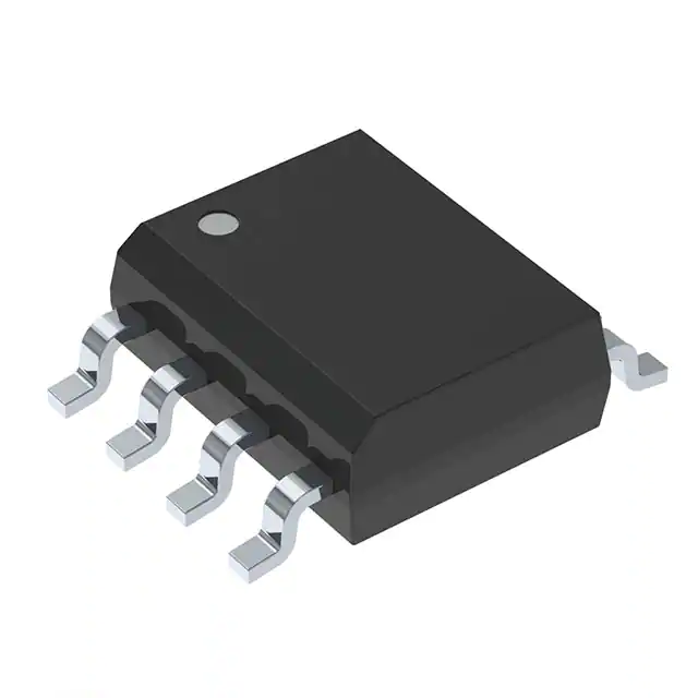
Surface Mount
Available in Tape & Reel
150°C Operating Temperature
Lead-Free
S1
1
8
D1
G1
2
7
D1
S2
3
6
D2
G2
4
5
D2
Description
VDSS = 30V
RDS(on) = 0.029Ω
Top View
These HEXFET® Power MOSFET's in a Dual
SO-8 package utilize the lastest processing
techniques to achieve extremely low on-resistance
per silicon area. Additional features of these
HEXFET Power MOSFET's are a 150°C junction
operating temperature, fast switching speed and
improved repetitive avalanche rating. These
benefits combine to make this design an extremely
efficient and reliable device for use in a wide
variety of applications.
The efficient SO-8 package provides enhanced
thermal characteristics and dual MOSFET die
capability making it ideal in a variety of power
applications. This dual, surface mount SO-8 can
dramatically reduce board space and is also
available in Tape & Reel.
SO-8
Absolute Maximum Ratings ( TA = 25°C Unless Otherwise Noted)
Drain-Source Voltage
Gate-Source Voltage
Continuous Drain Current
TA = 25°C
TA = 70°C
Pulsed Drain Current
Continuous Source Current (Diode Conduction)
TA = 25°C
Maximum Power Dissipation
TA = 70°C
Single Pulse Avalanche Energy
Avalanche Current
Repetitive Avalanche Energy
Peak Diode Recovery dv/dt
Junction and Storage Temperature Range
Symbol
Maximum
VDS
V GS
30
± 20
6.5
5.2
30
2.5
2.0
1.3
82
4.0
0.20
5.8
-55 to + 150
ID
IDM
IS
PD
EAS
IAR
EAR
dv/dt
TJ, TSTG
Units
V
A
W
mJ
A
mJ
V/ ns
°C
Thermal Resistance Ratings
Parameter
Maximum Junction-to-Ambient
www.irf.com
Symbol
Limit
Units
RθJA
62.5
°C/W
1
08/02/10
�IRF7313QPbF
Electrical Characteristics @ TJ = 25°C (unless otherwise specified)
∆V(BR)DSS/∆TJ
Parameter
Drain-to-Source Breakdown Voltage
Breakdown Voltage Temp. Coefficient
RDS(on)
Static Drain-to-Source On-Resistance
VGS(th)
gfs
Gate Threshold Voltage
Forward Transconductance
IDSS
Drain-to-Source Leakage Current
V(BR)DSS
I GSS
Qg
Qgs
Qgd
td(on)
tr
td(off)
tf
Ciss
Coss
Crss
Gate-to-Source Forward Leakage
Gate-to-Source Reverse Leakage
Total Gate Charge
Gate-to-Source Charge
Gate-to-Drain ("Miller") Charge
Turn-On Delay Time
Rise Time
Turn-Off Delay Time
Fall Time
Input Capacitance
Output Capacitance
Reverse Transfer Capacitance
Min.
30
1.0
Typ. Max. Units
Conditions
V
V GS = 0V, ID = 250µA
0.022 V/°C Reference to 25°C, ID = 1mA
0.023 0.029
V GS = 10V, ID = 5.8A
Ω
0.032 0.046
V GS = 4.5V, ID = 4.7A
V
V DS = V GS, ID = 250µA
14
S
V DS = 15V, ID = 5.8A
1.0
V DS = 24V, VGS = 0V
µA
25
V DS = 24V, VGS = 0V, TJ = 55°C
100
V GS = 20V
nA
-100
V GS = -20V
22
33
I D = 5.8A
2.6 3.9
nC V DS = 15V
6.4 9.6
V GS = 10V, See Fig. 10
8.1
12
V DD = 15V
8.9
13
I D = 1.0A
ns
26
39
R G = 6.0Ω
17
26
R D = 15Ω
650
V GS = 0V
320
pF
V DS = 25V
130
= 1.0MHz, See Fig. 9
Source-Drain Ratings and Characteristics
IS
I SM
VSD
trr
Qrr
Parameter
Continuous Source Current
(Body Diode)
Pulsed Source Current
(Body Diode)
Diode Forward Voltage
Reverse Recovery Time
Reverse RecoveryCharge
Min. Typ. Max. Units
2.5
30
0.78
45
58
1.0
68
87
A
V
ns
nC
Conditions
MOSFET symbol
showing the
G
integral reverse
p-n junction diode.
TJ = 25°C, IS = 1.7A, VGS = 0V
TJ = 25°C, IF = 1.7A
di/dt = 100A/µs
D
S
Notes:
Repetitive rating; pulse width limited by
max. junction temperature. ( See fig. 11 )
Starting TJ = 25°C, L = 10mH
R G = 25Ω, IAS = 4.0A.
www.irf.com
ISD ≤ 4.0A, di/dt ≤ 74A/µs, VDD ≤ V(BR)DSS, TJ ≤ 150°C
Pulse width ≤ 300µs; duty cycle ≤ 2%.
Surface mounted on FR-4 board, t ≤ 10sec.
2
�IRF7313QPbF
100
100
VGS
15V
10V
7.0V
5.5V
4.5V
4.0V
3.5V
BOTTOM 3.0V
VGS
15V
10V
7.0V
5.5V
4.5V
4.0V
3.5V
BOTTOM 3.0V
TOP
I D, Drain-to-Source Current (A)
I D , Drain-to-Source Current (A)
TOP
10
3.0V
20µs PULSE WIDTH
TJ = 25°C
A
1
0.1
1
10
3.0V
20µs PULSE WIDTH
TJ = 150°C
A
1
0.1
10
Fig 1. Typical Output Characteristics
10
Fig 2. Typical Output Characteristics
100
100
ISD , Reverse Drain Current (A)
I D , Drain-to-Source Current (A)
1
VDS, Drain-to-Source Voltage (V)
V DS , Drain-to-Source Voltage (V)
TJ = 25°C
TJ = 150°C
10
VDS = 10V
20µs PULSE WIDTH
1
3.0
3.5
4.0
4.5
VGS , Gate-to-Source Voltage (V)
Fig 3. Typical Transfer Characteristics
www.irf.com
A
5.0
TJ = 150°C
10
TJ = 25°C
VGS = 0V
1
0.4
0.6
0.8
1.0
1.2
1.4
A
1.6
V SD , Source-to-Drain Voltage (V)
Fig 4. Typical Source-Drain Diode
Forward Voltage
3
�RDS(on) , Drain-to-Source On Resistance
(Normalized)
2.0
RDS (on) , Drain-to-Source On Resistance (Ω)
IRF7313QPbF
ID = 5.8A
1.5
1.0
0.5
0.0
-60 -40 -20
VGS = 10V
0
20
40
60
0.040
0.032
0.028
0.024
0
0.08
0.06
I D = 5.8A
0.04
0.02
0.00
12
V GS , Gate-to-Source Voltage (V)
Fig 7. Typical On-Resistance Vs. Gate
Voltage
www.irf.com
15
A
E AS , Single Pulse Avalanche Energy (mJ)
RDS (on) , Drain-to-Source On Resistance (Ω)
0.10
9
20
30
40
A
Fig 6. Typical On-Resistance Vs. Drain
Current
0.12
6
10
I D , Drain Current (A)
Fig 5. Normalized On-Resistance
Vs. Temperature
3
V GS = 10V
0.020
80 100 120 140 160
TJ , Junction Temperature ( °C)
0
V GS = 4.5V
0.036
200
TOP
BOTTOM
160
IIDD
1.8A
3.2A
4.0A
120
80
40
A
0
25
50
75
100
125
150
Starting T J , Junction Temperature (°C)
Fig 8. Maximum Avalanche Energy
Vs. Drain Current
4
�IRF7313QPbF
20
V GS = 0V,
f = 1MHz
C iss = Cgs + C gd , Cds SHORTED
C rss = C gd
C oss = C ds + C gd
900
VGS , Gate-to-Source Voltage (V)
C, Capacitance (pF)
1200
Ciss
Coss
600
Crss
300
0
1
10
100
A
ID = 5.8A
VDS = 15V
16
12
8
4
0
0
10
20
30
40
QG , Total Gate Charge (nC)
VDS , Drain-to-Source Voltage (V)
Fig 9. Typical Capacitance Vs.
Drain-to-Source Voltage
Fig 10. Typical Gate Charge Vs.
Gate-to-Source Voltage
Thermal Response (Z thJA )
100
0.50
0.20
10
0.10
0.05
0.02
1
PDM
0.01
t1
t2
Notes:
1. Duty factor D = t 1 / t 2
2. Peak TJ = P DM x Z thJA + TA
SINGLE PULSE
(THERMAL RESPONSE)
0.1
0.00001
0.0001
0.001
0.01
0.1
1
10
100
t1 , Rectangular Pulse Duration (sec)
Fig 11. Maximum Effective Transient Thermal Impedance, Junction-to-Ambient
www.irf.com
5
�IRF7313QPbF
SO-8 Package Outline
Dimensions are shown in millimeters (inches)
D
DIM
B
5
A
8
6
7
6
H
E
1
2
3
0.25 [.010]
4
A
MIN
.0532
.0688
1.35
1.75
A1 .0040
.0098
0.10
0.25
b
.013
.020
0.33
0.51
c
.0075
.0098
0.19
0.25
D
.189
.1968
4.80
5.00
E
.1497
.1574
3.80
4.00
e
.050 BASIC
1.27 BASIC
e1
6X
e
e1
MAX
.025 BASIC
0.635 BASIC
H
.2284
.2440
5.80
6.20
K
.0099
.0196
0.25
0.50
L
.016
.050
0.40
1.27
y
0°
8°
0°
8°
K x 45°
C
y
0.10 [.004]
A1
8X b
0.25 [.010]
A
MILLIMETERS
MAX
A
5
INCHES
MIN
8X L
8X c
7
C A B
FOOT PRINT
NOT ES :
1. DIMENS IONING & T OLERANCING PER AS ME Y14.5M-1994.
8X 0.72 [.028]
2. CONT ROLLING DIMENS ION: MILLIMET ER
3. DIMENS IONS ARE S HOWN IN MILLIMET ERS [INCHES ].
4. OUT LINE CONFORMS T O JEDEC OUT LINE MS -012AA.
5 DIMENS ION DOES NOT INCLUDE MOLD PROT RUS IONS .
MOLD PROT RUS IONS NOT T O EXCEED 0.15 [.006].
6 DIMENS ION DOES NOT INCLUDE MOLD PROT RUS IONS .
MOLD PROT RUS IONS NOT T O EXCEED 0.25 [.010].
6.46 [.255]
7 DIMENS ION IS T HE LENGT H OF LEAD FOR S OLDERING T O
A S UBS T RAT E.
3X 1.27 [.050]
8X 1.78 [.070]
SO-8 Part Marking
EXAMPLE: T HIS IS AN IRF7101 (MOS FET )
INT ERNAT IONAL
RECT IFIER
LOGO
XXXX
F7101
DAT E CODE (YWW)
P = DES IGNAT ES LEAD-FREE
PRODUCT (OPTIONAL)
Y = LAS T DIGIT OF T HE YEAR
WW = WEEK
A = ASS EMBLY SIT E CODE
LOT CODE
PART NUMBER
Notes:
1. For an Automotive Qualified version of this part please seehttp://www.irf.com/product-info/auto/
2. For the most current drawing please refer to IR website at http://www.irf.com/package/
www.irf.com
6
�IRF7313QPbF
SO-8 Tape and Reel
Dimensions are shown in millimeters (inches)
TERMINAL NUMBER 1
12.3 ( .484 )
11.7 ( .461 )
8.1 ( .318 )
7.9 ( .312 )
FEED DIRECTION
NOTES:
1. CONTROLLING DIMENSION : MILLIMETER.
2. ALL DIMENSIONS ARE SHOWN IN MILLIMETERS(INCHES).
3. OUTLINE CONFORMS TO EIA-481 & EIA-541.
330.00
(12.992)
MAX.
14.40 ( .566 )
12.40 ( .488 )
NOTES :
1. CONTROLLING DIMENSION : MILLIMETER.
2. OUTLINE CONFORMS TO EIA-481 & EIA-541.
Data and specifications subject to change without notice.
This product has been designed and qualified for the Industrial market.
Qualification Standards can be found on IR’s Web site.
IR WORLD HEADQUARTERS: 233 Kansas St., El Segundo, California 90245, USA Tel: (310) 252-7105
TAC Fax: (310) 252-7903
Visit us at www.irf.com for sales contact information.08/2010
www.irf.com
7
�


 工商网监
湘ICP备2023018690号
工商网监
湘ICP备2023018690号