IRF7313PbF-1
HEXFET® Power MOSFET
VDS
RDS(on) max
(@VGS = 10V)
30
V
0.029
Ω
22
Qg (typical)
ID
nC
6.5
(@TA = 25°C)
1
8
D1
G1
2
7
D1
S2
3
6
D2
4
5
D2
S1
G2
A
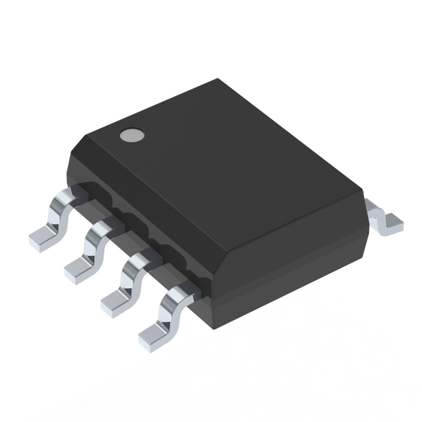
SO-8
Top View
Features
Industry-standard pinout SO-8 Package
Compatible with Existing Surface Mount Techniques
RoHS Compliant, Halogen-Free
MSL1, Industrial qualification
Base Part Number
Package Type
IRF7313PbF-1
SO-8
⇒
Benefits
Multi-Vendor Compatibility
Easier Manufacturing
Environmentally Friendlier
Increased Reliability
Standard Pack
Form
Quantity
Tube/Bulk
95
Tape and Reel
4000
Orderable Part Number
IRF7313PbF-1
IRF7313TRPbF-1
Absolute Maximum Ratings ( TA = 25°C Unless Otherwise Noted)
Drain-Source Voltage
Gate-Source Voltage
Continuous Drain Current
TA = 25°C
TA = 70°C
Pulsed Drain Current
Continuous Source Current (Diode Conduction)
TA = 25°C
Maximum Power Dissipation
TA = 70°C
Single Pulse Avalanche Energy
Avalanche Current
Repetitive Avalanche Energy
Peak Diode Recovery dv/dt
Junction and Storage Temperature Range
Symbol
Maximum
VDS
VGS
30
± 20
6.5
5.2
30
2.5
2.0
1.3
82
4.0
0.20
5.8
-55 to + 150
ID
I DM
IS
PD
EAS
IAR
EAR
dv/dt
TJ, TSTG
Units
V
A
W
mJ
A
mJ
V/ ns
°C
Thermal Resistance Ratings
Parameter
Maximum Junction-to-Ambient
1
Symbol
Limit
Units
RθJA
62.5
°C/W
www.irf.com © 2013 International Rectifier Submit Datasheet Feedback
November 14, 2013
�IRF7313PbF-1
Electrical Characteristics @ TJ = 25°C (unless otherwise specified)
ΔV(BR)DSS/ΔTJ
Parameter
Drain-to-Source Breakdown Voltage
Breakdown Voltage Temp. Coefficient
RDS(on)
Static Drain-to-Source On-Resistance
VGS(th)
gfs
Gate Threshold Voltage
Forward Transconductance
IDSS
Drain-to-Source Leakage Current
V(BR)DSS
I GSS
Qg
Qgs
Qgd
td(on)
tr
td(off)
tf
Ciss
Coss
Crss
Gate-to-Source Forward Leakage
Gate-to-Source Reverse Leakage
Total Gate Charge
Gate-to-Source Charge
Gate-to-Drain ("Miller") Charge
Turn-On Delay Time
Rise Time
Turn-Off Delay Time
Fall Time
Input Capacitance
Output Capacitance
Reverse Transfer Capacitance
Min.
30
1.0
Typ. Max. Units
Conditions
V
V GS = 0V, ID = 250µA
0.022 V/°C Reference to 25°C, ID = 1mA
0.023 0.029
V GS = 10V, ID = 5.8A
Ω
0.032 0.046
V GS = 4.5V, ID = 4.7A
V
V DS = V GS, ID = 250µA
14
S
V DS = 15V, ID = 5.8A
1.0
V DS = 24V, VGS = 0V
µA
25
V DS = 24V, VGS = 0V, TJ = 55°C
100
V GS = 20V
nA
-100
V GS = -20V
22
33
I D = 5.8A
2.6 3.9
nC V DS = 15V
6.4 9.6
V GS = 10V, See Fig. 10
8.1
12
V DD = 15V
8.9
13
I D = 1.0A
ns
26
39
R G = 6.0Ω
17
26
R D = 15Ω
650
V GS = 0V
320
pF
V DS = 25V
130
= 1.0MHz, See Fig. 9
Source-Drain Ratings and Characteristics
IS
I SM
VSD
trr
Qrr
Parameter
Continuous Source Current
(Body Diode)
Pulsed Source Current
(Body Diode)
Diode Forward Voltage
Reverse Recovery Time
Reverse RecoveryCharge
Min. Typ. Max. Units
2.5
30
0.78
45
58
1.0
68
87
A
V
ns
nC
Conditions
MOSFET symbol
showing the
G
integral reverse
p-n junction diode.
TJ = 25°C, IS = 1.7A, VGS = 0V
TJ = 25°C, IF = 1.7A
di/dt = 100A/µs
D
S
Notes:
Repetitive rating; pulse width limited by max. junction temperature. ( See fig. 11 )
Starting TJ = 25°C, L = 10mH, RG = 25Ω, IAS = 4.0A.
ISD ≤ 4.0A, di/dt ≤ 74A/µs, VDD ≤ V(BR)DSS, TJ ≤ 150°C
Pulse width ≤ 300µs; duty cycle ≤ 2%.
Surface mounted on FR-4 board, t ≤ 10sec.
2
www.irf.com © 2013 International Rectifier Submit Datasheet Feedback
November 14, 2013
�IRF7313PbF-1
100
100
VGS
15V
10V
7.0V
5.5V
4.5V
4.0V
3.5V
BOTTOM 3.0V
VGS
15V
10V
7.0V
5.5V
4.5V
4.0V
3.5V
BOTTOM 3.0V
TOP
I D, Drain-to-Source Current (A)
I D , Drain-to-Source Current (A)
TOP
10
3.0V
20μs PULSE WIDTH
TJ = 25°C
A
1
0.1
1
10
3.0V
20μs PULSE WIDTH
TJ = 150°C
A
1
0.1
10
1
10
VDS, Drain-to-Source Voltage (V)
V DS , Drain-to-Source Voltage (V)
Fig 1. Typical Output Characteristics
Fig 2. Typical Output Characteristics
VDS
100
ISD , Reverse Drain Current (A)
I D , Drain-to-Source Current (A)
100
TJ = 25°C
TJ = 150°C
10
VDS = 10V
20μs PULSE WIDTH
1
3.0
3.5
4.0
4.5
VGS , Gate-to-Source Voltage (V)
Fig 3. Typical Transfer Characteristics
3
A
5.0
TJ = 150°C
10
TJ = 25°C
VGS = 0V
1
0.4
0.6
0.8
1.0
1.2
1.4
V SD , Source-to-Drain Voltage (V)
Fig 4. Typical Source-Drain Diode
Forward Voltage
www.irf.com © 2013 International Rectifier Submit Datasheet Feedback
A
1.6
November 14, 2013
�RDS(on) , Drain-to-Source On Resistance
(Normalized)
2.0
RDS (on) , Drain-to-Source On Resistance (Ω)
IRF7313PbF-1
ID = 5.8A
1.5
1.0
0.5
0.0
-60 -40 -20
VGS = 10V
0
20
40
60
0.040
0.032
0.028
0.024
0
0.08
0.06
I D = 5.8A
0.04
0.02
0.00
12
V GS , Gate-to-Source Voltage (V)
Fig 7. Typical On-Resistance Vs. Gate
Voltage
4
15
A
E AS , Single Pulse Avalanche Energy (mJ)
RDS (on) , Drain-to-Source On Resistance (Ω)
0.10
9
20
30
40
A
Fig 6. Typical On-Resistance Vs. Drain
Current
0.12
6
10
I D , Drain Current (A)
Fig 5. Normalized On-Resistance
Vs. Temperature
3
V GS = 10V
0.020
80 100 120 140 160
TJ , Junction Temperature ( °C)
0
V GS = 4.5V
0.036
200
TOP
BOTTOM
160
IIDD
1.8A
3.2A
4.0A
120
80
40
0
25
50
75
100
125
Starting T J , Junction Temperature (°C)
Fig 8. Maximum Avalanche Energy
Vs. Drain Current
www.irf.com © 2013 International Rectifier Submit Datasheet Feedback
A
150
November 14, 2013
�IRF7313PbF-1
20
V GS = 0V,
f = 1MHz
C iss = Cgs + C gd , Cds SHORTED
C rss = C gd
C oss = C ds + C gd
900
VGS , Gate-to-Source Voltage (V)
C, Capacitance (pF)
1200
Ciss
Coss
600
Crss
300
0
1
10
100
A
ID = 5.8A
VDS = 15V
16
12
8
4
0
0
10
20
30
40
QG , Total Gate Charge (nC)
VDS , Drain-to-Source Voltage (V)
Fig 9. Typical Capacitance Vs.
Drain-to-Source Voltage
Fig 10. Typical Gate Charge Vs.
Gate-to-Source Voltage
Thermal Response (Z thJA )
100
0.50
0.20
10
0.10
0.05
0.02
1
PDM
0.01
t1
t2
Notes:
1. Duty factor D = t 1 / t 2
2. Peak TJ = P DM x Z thJA + TA
SINGLE PULSE
(THERMAL RESPONSE)
0.1
0.00001
0.0001
0.001
0.01
0.1
1
10
100
t1 , Rectangular Pulse Duration (sec)
Fig 11. Maximum Effective Transient Thermal Impedance, Junction-to-Ambient
5
www.irf.com © 2013 International Rectifier Submit Datasheet Feedback
November 14, 2013
�IRF7313PbF-1
SO-8 Package Outline
Dimensions are shown in milimeters (inches)
D
DIM
B
5
A
A
INCHES
MAX
MIN
.0532
.0688
1.35
A1 .0040
8
6
7
6
5
H
E
1
2
3
0.25 [.010]
4
A
e
e1
8X b
0.25 [.010]
A
.0098
0.10
MAX
1.75
0.25
b
.013
.020
0.33
0.51
c
.0075
.0098
0.19
0.25
D
.189
.1968
4.80
5.00
E
.1497
.1574
3.80
4.00
e
.050 BASIC
1.27 BASIC
e1
6X
MILLIMET ERS
MIN
.025 BASIC
0.635 BAS IC
H
.2284
.2440
5.80
6.20
K
.0099
.0196
0.25
0.50
L
.016
.050
0.40
1.27
y
0°
8°
0°
8°
K x 45°
C
y
0.10 [.004]
A1
8X L
8X c
7
C A B
FOOT PRINT
NOT ES :
1. DIMENS IONING & T OLERANCING PER AS ME Y14.5M-1994.
8X 0.72 [.028]
2. CONT ROLLING DIMENS ION: MILLIMETER
3. DIMENS IONS ARE SHOWN IN MILLIMET ERS [INCHES ].
4. OUT LINE CONFORMS T O JEDEC OUT LINE MS-012AA.
5 DIMENS ION DOES NOT INCLUDE MOLD PROT RUSIONS .
MOLD PROT RUSIONS NOT T O EXCEED 0.15 [.006].
6 DIMENS ION DOES NOT INCLUDE MOLD PROT RUSIONS .
MOLD PROT RUSIONS NOT T O EXCEED 0.25 [.010].
6.46 [.255]
7 DIMENS ION IS T HE LENGT H OF LEAD FOR SOLDERING T O
A S UBS T RAT E.
3X 1.27 [.050]
8X 1.78 [.070]
SO-8 Part Marking Information (Lead-Free)
EXAMPLE: T HIS IS AN IRF7101 (MOSFET )
INTERNAT IONAL
RECT IFIER
LOGO
XXXX
F7101
DAT E CODE (YWW)
P = DESIGNAT ES LEAD-FREE
PRODUCT (OPT IONAL)
Y = LAST DIGIT OF T HE YEAR
WW = WEEK
A = ASS EMBLY SIT E CODE
LOT CODE
PART NUMBER
Note: For the most current drawing please refer to IR website at http://www.irf.com/package/
6
www.irf.com © 2013 International Rectifier Submit Datasheet Feedback
November 14, 2013
�IRF7313PbF-1
SO-8 Tape and Reel (Dimensions are shown in milimeters (inches))
TERMINAL NUMBER 1
12.3 ( .484 )
11.7 ( .461 )
8.1 ( .318 )
7.9 ( .312 )
FEED DIRECTION
NOTES:
1. CONTROLLING DIMENSION : MILLIMETER.
2. ALL DIMENSIONS ARE SHOWN IN MILLIMETERS(INCHES).
3. OUTLINE CONFORMS TO EIA-481 & EIA-541.
330.00
(12.992)
MAX.
14.40 ( .566 )
12.40 ( .488 )
NOTES :
1. CONTROLLING DIMENSION : MILLIMETER.
2. OUTLINE CONFORMS TO EIA-481 & EIA-541.
Note: For the most current drawing please refer to IR website at http://www.irf.com/package/
†
Qualification information
Industrial
Qualification level
Moisture Sensitivity Level
RoHS compliant
(per JEDE C JE S D47F
SO-8
††
guidelines)
MS L1
††
(per JEDE C J-S T D-020D )
Yes
† Qualification standards can be found at International Rectifier’s web site: http://www.irf.com/product-info/reliability
†† Applicable version of JEDEC standard at the time of product release
IR WORLD HEADQUARTERS: 101 N. Sepulveda Blvd., El Segundo, California 90245, USA
To contact International Rectifier, please visit http://www.irf.com/whoto-call/
7
www.irf.com © 2013 International Rectifier Submit Datasheet Feedback
November 14, 2013
�