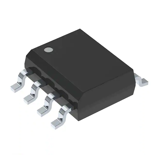
IRF7341GPbF
• Advanced Process Technology
• ÿDual N-Channel MOSFET
• ÿUltra Low On-Resistance
• ÿ175°C Operating Temperature
• ÿ Repetitive Avalanche Allowed up to Tjmax
• ÿLead-Free
• ÿHalogen-Free
VDSS
55V
Description
These HEXFET ® Power MOSFET’s in a Dual SO-8 package
utilize the lastest processing techniques to achieve extremely
low on-resistance per silicon area. Additional features of these
HEXFET Power MOSFET’s are a 175°C junction operating
temperature, fast switching speed and improved repetitive
avalanche rating. These benefits combine to make this design
an extremely efficient and reliable device for use in a wide
variety of other applications.
The 175°C rating for the SO-8 package provides improved
thermal performance with increased safe operating area and
dual MOSFET die capability make it ideal in a variety of power
applications. This dual, surface mount SO-8 can dramatically
reduce board space and is also available in Tape & Reel.
Base Part Number
Package Type
IRF7341GPbF
SO-8
HEXFET® Power MOSFET
RDS(on) max
ID
0.050@VGS = 10V
5.1A
0.065@VGS = 4.5V
4.42A
S1
1
8
D1
G1
2
7
D1
S2
3
6
D2
4
5
D2
G2
SO-8
Top View
Standard Pack
Form
Quantity
Tube/Bulk
95
Tape and Reel
4000
Orderable Part Number
IRF7341GPbF
IRF7341GTRPbF
Absolute Maximum Ratings
Parameter
VDS
ID @ TA = 25°C
ID @ TA = 70°C
IDM
PD @TA = 25°C
PD @TA = 70°C
VGS
EAS
IAR
EAR
TJ , TSTG
Max.
Drain-Source Voltage
Continuous Drain Current, VGS @ 10V
Continuous Drain Current, VGS @ 10V
Pulsed Drain Current
Maximum Power Dissipation
Maximum Power Dissipation
Linear Derating Factor
Gate-to-Source Voltage
Single Pulse Avalanche Energy
Avalanche Current
Repetitive Avalanche Energy
Junction and Storage Temperature Range
Units
55
5.1
4.2
42
2.4
1.7
16
± 20
140
5.1
See Fig. 14, 15, 16
-55 to + 175
V
A
W
W
mW/°C
V
mJ
A
mJ
°C
Thermal Resistance
Parameter
RθJA
1
Maximum Junction-to-Ambient
www.irf.com © 2014 International Rectifier
Max.
Units
62.5
°C/W
Submit Datasheet Feedback
February 20, 2014
�IRF7341GPbF
Electrical Characteristics @ TJ = 25°C (unless otherwise specified)
ΔV(BR)DSS/ΔTJ
Parameter
Drain-to-Source Breakdown Voltage
Breakdown Voltage Temp. Coefficient
RDS(on)
Static Drain-to-Source On-Resistance
VGS(th)
gfs
Gate Threshold Voltage
Forward Transconductance
IDSS
Drain-to-Source Leakage Current
V(BR)DSS
IGSS
Qg
Qgs
Qgd
td(on)
tr
td(off)
tf
Ciss
Coss
Crss
Gate-to-Source Forward Leakage
Gate-to-Source Reverse Leakage
Total Gate Charge
Gate-to-Source Charge
Gate-to-Drain ("Miller") Charge
Turn-On Delay Time
Rise Time
Turn-Off Delay Time
Fall Time
Input Capacitance
Output Capacitance
Reverse Transfer Capacitance
Min.
55
–––
–––
1.0
10.4
–––
–––
–––
–––
–––
–––
–––
–––
–––
–––
–––
–––
–––
–––
Typ.
–––
0.052
0.043
0.056
–––
–––
–––
–––
–––
–––
29
2.9
7.3
9.2
7.7
31
12.5
780
190
66
Max. Units
Conditions
–––
V
VGS = 0V, ID = 250μA
––– V/°C Reference to 25°C, ID = 1mA
0.050
VGS = 10V, ID = 5.1A
Ω
0.065
VGS = 4.5V, ID = 4.42A
–––
V
VDS = VGS, ID = 250μA
–––
S
VDS = 10V, ID = 5.2A
2.0
VDS = 44V, VGS = 0V
µA
25
VDS = 44V, VGS = 0V, TJ = 150°C
100
VGS = 20V
nA
-100
VGS = -20V
44
ID = 5.2A
4.4
nC
VDS = 44V
11
VGS = 10V
–––
VDD = 28V
–––
ID = 1.0A
ns
–––
RG = 6.0Ω
–––
VGS = 10V
–––
VGS = 0V
–––
pF
VDS = 25V
–––
ƒ = 1.0MHz
Source-Drain Ratings and Characteristics
IS
ISM
VSD
trr
Qrr
Parameter
Continuous Source Current
(Body Diode)
Pulsed Source Current
(Body Diode)
Diode Forward Voltage
Reverse Recovery Time
Reverse Recovery Charge
Min. Typ. Max. Units
2.4
42
–––
–––
–––
–––
51
76
1.2
77
114
A
V
ns
nC
Conditions
D
MOSFET symbol
showing the
G
integral reverse
p-n junction diode.
S
TJ = 25°C, IS = 2.6A, VGS = 0V
TJ = 25°C, IF = 2.6A
di/dt = 100A/μs
Notes:
Repetitive rating; pulse width limited by
max. junction temperature.
Surface mounted on FR-4 board, t ≤ 10sec.
Pulse width ≤ 300μs; duty cycle ≤ 2%.
2
www.irf.com © 2014 International Rectifier
Submit Datasheet Feedback
February 20, 2014
�IRF7341GPbF
100
VGS
15.0V
10.0V
7.0V
5.5V
4.5V
4.0V
3.5V
BOTTOM 2.7V
100
VGS
15.0V
10.0V
7.0V
5.5V
4.5V
4.0V
3.5V
BOTTOM 2.7V
10
2.7V
1
TOP
ID, Drain-to-Source Current (A)
ID, Drain-to-Source Current (A)
TOP
10
2.7V
1
20μs PULSE WIDTH
Tj = 175°C
20μs PULSE WIDTH
Tj = 25°C
0.1
0.1
0.1
1
10
100
0.1
VDS, Drain-to-Source Voltage (V)
2.5
R DS(on) , Drain-to-Source On Resistance
(Normalized)
I D , Drain-to-Source Current (A)
TJ = 25 ° C
TJ = 175 ° C
10
V DS = 25V
20μs PULSE WIDTH
4.0
5.0
6.0
7.0
VGS , Gate-to-Source Voltage (V)
Fig 3. Typical Transfer Characteristics
3
100
Fig 2. Typical Output Characteristics
100
3.0
10
VDS, Drain-to-Source Voltage (V)
Fig 1. Typical Output Characteristics
1
2.0
1
ID = 5.2A
2.0
1.5
1.0
0.5
0.0
-60 -40 -20 0
VGS = 10V
20 40 60 80 100 120 140 160 180
TJ , Junction Temperature ( °C)
Fig 4. Normalized On-Resistance
Vs. Temperature
www.irf.com © 2014 International Rectifier Submit Datasheet Feedback
February 20, 2014
�IRF7341GPbF
VGS = 0V,
f = 1 MHZ
C iss
= Cgs + Cgd ,
SHORTED
Cds
Crss = Cgd
Coss = Cds + Cgd
1000
Ciss
800
600
400
Coss
200
ID = 5.2A
VDS = 44V
VDS = 27V
VDS = 11V
16
12
8
4
Crss
0
1
10
0
100
0
10
30
40
50
Fig 6. Typical Gate Charge Vs.
Gate-to-Source Voltage
Fig 5. Typical Capacitance Vs.
Drain-to-Source Voltage
100
1000
OPERATION IN THIS AREA LIMITED
BY RDS(on)
TJ = 175 ° C
I D , Drain Current (A)
100
10
TJ = 25 ° C
1
0.1
0.2
V GS = 0 V
0.5
0.8
1.1
1.4
VSD ,Source-to-Drain Voltage (V)
Fig 7. Typical Source-Drain Diode
Forward Voltage
4
20
QG , Total Gate Charge (nC)
VDS, Drain-to-Source Voltage (V)
ISD , Reverse Drain Current (A)
C, Capacitance(pF)
1200
20
VGS , Gate-to-Source Voltage (V)
1400
www.irf.com © 2014 International Rectifier
10us
100us
10
1ms
10ms
1
TC = 25 ° C
TJ = 175 ° C
Single Pulse
0.1
0.1
1
10
100
VDS , Drain-to-Source Voltage (V)
Fig 8. Maximum Safe Operating Area
Submit Datasheet Feedback
February 20, 2014
1000
�IRF7341GPbF
6.0
RD
V DS
VGS
I D , Drain Current (A)
5.0
D.U.T.
RG
+
- VDD
4.0
10V
3.0
Pulse Width ≤ 1 µs
Duty Factor ≤ 0.1 %
2.0
Fig 10a. Switching Time Test Circuit
1.0
VDS
90%
0.0
25
50
75
100
125
150
TC , Case Temperature ( °C)
175
10%
VGS
Fig 9. Maximum Drain Current Vs.
Case Temperature
td(on)
tr
t d(off)
tf
Fig 10b. Switching Time Waveforms
100
Thermal Response (Z thJA )
D = 0.50
0.20
10
0.10
0.05
0.02
1
0.01
PDM
SINGLE PULSE
(THERMAL RESPONSE)
0.1
0.01
0.00001
t1
t2
Notes:
1. Duty factor D = t 1 / t 2
2. Peak T J = P DM x Z thJA + TA
0.0001
0.001
0.01
0.1
1
10
100
t1 , Rectangular Pulse Duration (sec)
Fig 10. Maximum Effective Transient Thermal Impedance, Junction-to-Ambient
5
www.irf.com © 2014 International Rectifier Submit Datasheet Feedback
February 20, 2014
�IRF7341GPbF
RDS ( on ) , Drain-to-Source On Resistance Ω
( )
(
RDS(on), Drain-to -Source On ResistanceΩ)
0.070
0.060
0.050
0.040
ID = 7.1A
0.030
0.020
2.0
4.0
6.0
8.0
10.0
12.0
14.0
0.100
0.080
0.060
VGS = 4.5V
0.040
VGS = 10V
0.020
16.0
0
10
VGS, Gate -to -Source Voltage (V)
20
30
40
50
60
ID , Drain Current ( A )
Fig 11. Typical On-Resistance Vs.
Gate Voltage
Fig 12. Typical On-Resistance Vs.
Drain Current
QG
10 V
400
QGS
QGD
VG
Charge
Fig 13a. Basic Gate Charge Waveform
Current Regulator
Same Type as D.U.T.
50KΩ
.2μF
.3μF
D.U.T.
+
V
- DS
BOTTOM
240
160
80
0
25
VGS
50
75
100
125
Starting Tj, Junction Temperature
3mA
IG
ID
Current Sampling Resistors
Fig 13b. Gate Charge Test Circuit
6
EAS , Single Pulse Avalanche Energy (mJ)
320
12V
ID
2.1A
4.3A
5.1A
TOP
www.irf.com © 2014 International Rectifier
150
( ° C)
Fig 14. Maximum Avalanche Energy
Vs. Drain Current
Submit Datasheet Feedback
February 20, 2014
175
�IRF7341GPbF
100
Duty Cycle = Single Pulse
Avalanche Current (A)
10
1
0.01
0.1
0.05
0.10
Allowed avalanche Current vs
avalanche pulsewidth, tav
assuming Δ Tj = 25°C due to
avalanche losses
0.01
0.001
1.0E-06
1.0E-05
1.0E-04
1.0E-03
1.0E-02
1.0E-01
1.0E+00
1.0E+01
1.0E+02
tav (sec)
Fig 15. Typical Avalanche Current Vs.Pulsewidth
EAR , Avalanche Energy (mJ)
140
TOP
Single Pulse
BOTTOM 10% Duty Cycle
ID = 5.1A
120
100
80
60
40
20
0
25
50
75
100
125
150
Starting T J , Junction Temperature (°C)
Fig 16. Maximum Avalanche Energy
Vs. Temperature
7
Notes on Repetitive Avalanche Curves , Figures 15, 16:
(For further info, see AN-1005 at www.irf.com)
1. Avalanche failures assumption:
Purely a thermal phenomenon and failure occurs at a
temperature far in excess of T jmax. This is validated for
every part type.
2. Safe operation in Avalanche is allowed as long asTjmax is
not exceeded.
3. Equation below based on circuit and waveforms shown in
Figures 12a, 12b.
4. PD (ave) = Average power dissipation per single
avalanche pulse.
5. BV = Rated breakdown voltage (1.3 factor accounts for
voltage increase during avalanche).
6. Iav = Allowable avalanche current.
7. ΔT = Allowable rise in junction temperature, not to exceed
Tjmax (assumed as 25°C in Figure 15, 16).
tav = Average time in avalanche.
175
D = Duty cycle in avalanche = tav ·f
ZthJC(D, tav ) = Transient thermal resistance, see figure 11)
PD (ave) = 1/2 ( 1.3·BV·Iav) = DT/ ZthJC
Iav = 2DT/ [1.3·BV·Zth]
EAS (AR) = PD (ave)·tav
www.irf.com © 2014 International Rectifier Submit Datasheet Feedback
February 20, 2014
�IRF7341GPbF
SO-8 Package Outline(Mosfet & Fetky)
Dimensions are shown in milimeters (inches)
D
DIM
B
5
A
8
6
7
6
H
E
1
2
3
0.25 [.010]
4
A
MIN
.0532
.0688
1.35
1.75
A1 .0040
.0098
0.10
0.25
b
.013
.020
0.33
0.51
c
.0075
.0098
0.19
0.25
D
.189
.1968
4.80
5.00
E
.1497
.1574
3.80
4.00
e
.050 BAS IC
1.27 BASIC
e1
6X
e
e1
8X b
0.25 [.010]
A
MILLIMET ERS
MAX
A
5
INCHES
MIN
MAX
.025 BAS IC
0.635 BAS IC
H
.2284
.2440
5.80
6.20
K
.0099
.0196
0.25
0.50
L
.016
.050
0.40
1.27
y
0°
8°
0°
8°
K x 45°
C
A1
y
0.10 [.004]
C A B
8X L
8X c
7
FOOT PRINT
NOT ES:
8X 0.72 [.028]
1. DIMENS IONING & TOLERANCING PER AS ME Y14.5M-1994.
2. CONT ROLLING DIMENSION: MILLIMET ER
3. DIMENS IONS ARE SHOWN IN MILLIMET ERS [INCHES ].
4. OUT LINE CONFORMS T O JEDEC OUT LINE MS-012AA.
5 DIMENS ION DOES NOT INCLUDE MOLD PROT RUS IONS.
MOLD PROTRUSIONS NOT T O EXCEED 0.15 [.006].
6.46 [.255]
6 DIMENS ION DOES NOT INCLUDE MOLD PROT RUS IONS.
MOLD PROTRUSIONS NOT T O EXCEED 0.25 [.010].
7 DIMENS ION IS T HE LENGTH OF LEAD F OR S OLDERING TO
A SUBST RAT E.
3X 1.27 [.050]
8X 1.78 [.070]
SO-8 Part Marking Information
EXAMPLE: THIS IS AN IRF8707GPBF
INT ERNAT IONAL
RECTIFIER
LOGO
XXXX
F8707G
DAT E CODE (YWW)
P = DIS GNATES LEAD - FREE
PRODUCT
Y = LAS T DIGIT OF THE YEAR
WW = WEEK
A = AS S EMBLY S IT E CODE
LOT CODE
PART NUMBER (G DES IGNAT ES
HALOGEN-FREE
Note: For the most current drawing please refer to IR website at http://www.irf.com/package/
8
www.irf.com © 2014 International Rectifier
Submit Datasheet Feedback
February 20, 2014
�IRF7341GPbF
SO-8 Tape and Reel
Dimensions are shown in millimeters (inches)
TERMINAL NUMBER 1
12.3 ( .484 )
11.7 ( .461 )
8.1 ( .318 )
7.9 ( .312 )
FEED DIRECTION
NOTES:
1. CONTROLLING DIMENSION : MILLIMETER.
2. ALL DIMENSIONS ARE SHOWN IN MILLIMETERS(INCHES).
3. OUTLINE CONFORMS TO EIA-481 & EIA-541.
330.00
(12.992)
MAX.
14.40 ( .566 )
12.40 ( .488 )
NOTES :
1. CONTROLLING DIMENSION : MILLIMETER.
2. OUTLINE CONFORMS TO EIA-481 & EIA-541.
Note: For the most current drawing please refer to IR website at http://www.irf.com/package/
†
Qualification information
Industrial
Qualification level
Moisture Sensitivity Level
RoHS compliant
(per JEDE C JE S D47F
SO-8
††
guidelines)
MS L1
††
(per JEDE C J-S T D-020D )
Yes
† Qualification standards can be found at International Rectifier’s web site: http://www.irf.com/product-info/reliability
†† Applicable version of JEDEC standard at the time of product release
IR WORLD HEADQUARTERS: 101 N. Sepulveda Blvd., El Segundo, California 90245, USA
To contact International Rectifier, please visit http://www.irf.com/whoto-call/
9
www.irf.com © 2014 International Rectifier Submit Datasheet Feedback
February 20, 2014
�IMPORTANT NOTICE
The information given in this document shall in no
event be regarded as a guarantee of conditions or
characteristics (“Beschaffenheitsgarantie”) .
With respect to any examples, hints or any typical
values stated herein and/or any information
regarding the application of the product, Infineon
Technologies hereby disclaims any and all
warranties and liabilities of any kind, including
without limitation warranties of non-infringement
of intellectual property rights of any third party.
In addition, any information given in this document
is subject to customer’s compliance with its
obligations stated in this document and any
applicable legal requirements, norms and
standards concerning customer’s products and any
use of the product of Infineon Technologies in
customer’s applications.
The data contained in this document is exclusively
intended for technically trained staff. It is the
responsibility of customer’s technical departments
to evaluate the suitability of the product for the
intended application and the completeness of the
product information given in this document with
respect to such application.
For further information on the product, technology,
delivery terms and conditions and prices please
contact your nearest Infineon Technologies office
(www.infineon.com).
WARNINGS
Due to technical requirements products may
contain dangerous substances. For information on
the types in question please contact your nearest
Infineon Technologies office.
Except as otherwise explicitly approved by Infineon
Technologies in a written document signed by
authorized
representatives
of
Infineon
Technologies, Infineon Technologies’ products may
not be used in any applications where a failure of
the product or any consequences of the use thereof
can reasonably be expected to result in personal
injury.
�