IRF7457PbF-1
VDS
RDS(on) max
(@VGS = 10V)
RDS(on) max
(@VGS = 4.5V)
Qg (typical)
ID
(@TA = 25°C)
20
V
7.0
mΩ
10.5
mΩ
28
nC
15
A
HEXFET® Power MOSFET
A
A
D
S
1
8
S
2
7
D
S
3
6
D
G
4
5
D
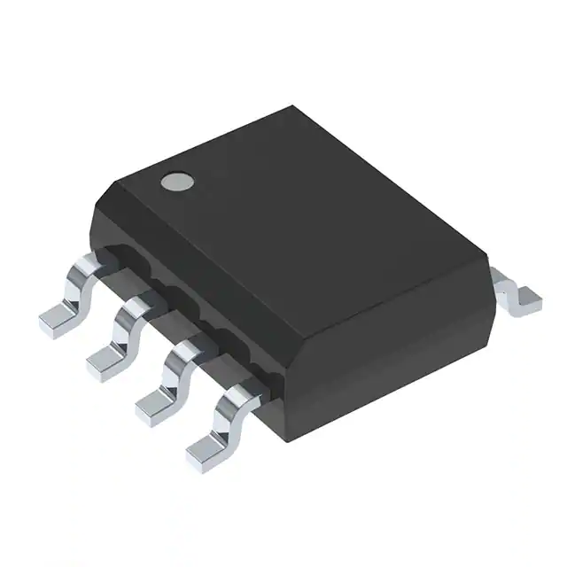
SO-8
Top View
Features
Benefits
Industry-standard pinout SO-8 Package
Compatible with Existing Surface Mount Techniques
RoHS Compliant, Halogen-Free
MSL1, Industrial qualification
Base Part Number
Package Type
IRF7457PbF-1
SO-8
⇒
Multi-Vendor Compatibility
Easier Manufacturing
Environmentally Friendlier
Increased Reliability
Standard Pack
Form
Quantity
Tube/Bulk
95
Tape and Reel
4000
Orderable Part Number
IRF7457PbF-1
IRF7457TRPbF-1
Absolute Maximum Ratings
Symbol
Parameter
VDS
VGS
ID @ TA = 25°C
ID @ TA = 70°C
IDM
PD @TA = 25°C
PD @TA = 70°C
TJ , TSTG
Drain-Source Voltage
Gate-to-Source Voltage
Continuous Drain Current, VGS @ 10V
Continuous Drain Current, VGS @ 10V
Pulsed Drain Current
Maximum Power Dissipation
Maximum Power Dissipation
Linear Derating Factor
Junction and Storage Temperature Range
Max.
Units
20
± 20
15
12
120
2.5
1.6
0.02
-55 to + 150
V
V
A
W
W
W/°C
°C
Thermal Resistance
Symbol
RθJL
RθJA
Parameter
Junction-to-Drain Lead
Junction-to-Ambient
Typ.
Max.
Units
–––
–––
20
50
°C/W
Notes through are on page 8
1
www.irf.com © 2014 International Rectifier
Submit Datasheet Feedback
June 30, 2014
�IRF7457PbF-1
Static @ TJ = 25°C (unless otherwise specified)
Parameter
Drain-to-Source Breakdown Voltage
ΔV(BR)DSS/ΔTJ Breakdown Voltage Temp. Coefficient
V(BR)DSS
RDS(on)
VGS(th)
IDSS
IGSS
Min.
20
–––
–––
Static Drain-to-Source On-Resistance
–––
Gate Threshold Voltage
1.0
–––
Drain-to-Source Leakage Current
–––
Gate-to-Source Forward Leakage
–––
Gate-to-Source Reverse Leakage
–––
Typ.
–––
0.023
5.5
8.0
–––
–––
–––
–––
–––
Max. Units
Conditions
–––
V
VGS = 0V, ID = 250μA
––– V/°C Reference to 25°C, I D = 1mA
7.0
VGS = 10V, ID = 15A
mΩ
10.5
VGS = 4.5V, ID = 12A
3.0
V
VDS = VGS, ID = 250μA
20
VDS = 16V, VGS = 0V
μA
100
VDS = 16V, VGS = 0V, TJ = 125°C
200
VGS = 16V
nA
-200
VGS = -16V
Dynamic @ TJ = 25°C (unless otherwise specified)
Symbol
gfs
Qg
Qgs
Qgd
Qoss
td(on)
tr
td(off)
tf
Ciss
Coss
Crss
Parameter
Forward Transconductance
Total Gate Charge
Gate-to-Source Charge
Gate-to-Drain ("Miller") Charge
Output Gate Charge
Turn-On Delay Time
Rise Time
Turn-Off Delay Time
Fall Time
Input Capacitance
Output Capacitance
Reverse Transfer Capacitance
Min.
30
–––
–––
–––
–––
–––
–––
–––
–––
–––
–––
–––
Typ.
–––
28
11
10
25
14
16
16
7.5
3100
1600
270
Max. Units
Conditions
–––
S
VDS = 16V, ID = 12A
42
ID = 12A
17
nC
VDS = 10V
15
VGS = 4.5V,
38
VGS = 0V, VDS = 10V
–––
VDD = 10V,
–––
ID = 12A
ns
–––
R G = 1.8Ω
–––
VGS = 4.5V
–––
VGS = 0V
–––
VDS = 10V
–––
pF
ƒ = 1.0MHz
Avalanche Characteristics
Parameter
EAS
IAR
Single Pulse Avalanche Energy
Avalanche Current
Typ.
Max.
Units
–––
–––
265
15
mJ
A
Diode Characteristics
Symbol
IS
ISM
Parameter
Continuous Source Current
(Body Diode)
Pulsed Source Current
(Body Diode)
VSD
Diode Forward Voltage
trr
Qrr
trr
Qrr
Reverse
Reverse
Reverse
Reverse
2
Recovery
Recovery
Recovery
Recovery
Time
Charge
Time
Charge
www.irf.com © 2014 International Rectifier
Min. Typ. Max. Units
–––
2.5
–––
120
––– 0.8
––– 0.67
––– 50
––– 70
––– 50
––– 74
1.3
–––
75
105
75
110
–––
A
–––
V
ns
nC
ns
nC
Conditions
D
MOSFET symbol
showing the
G
integral reverse
S
p-n junction diode.
TJ = 25°C, IS = 12A, VGS = 0V
TJ = 125°C, IS = 12A, VGS = 0V
TJ = 25°C, IF = 12A, VR= 15V
di/dt = 100A/μs
TJ = 125°C, IF = 12A, VR=15V
di/dt = 100A/μs
Submit Datasheet Feedback
June 30, 2014
�IRF7457PbF-1
1000
1000
VGS
15V
10V
7.0V
5.5V
4.5V
4.0V
3.5V
BOTTOM 2.7V
I D , Drain-to-Source Current (A)
I D , Drain-to-Source Current (A)
100
2.7V
10
100
20μs PULSE WIDTH
TJ = 25 °C
1
0.1
1
10
RDS(on) , Drain-to-Source On Resistance
(Normalized)
2.0
100
TJ = 150 ° C
10
TJ = 25 ° C
1
V DS = 15V
20μs PULSE WIDTH
3.0
3.5
4.0
20μs PULSE WIDTH
TJ = 150 °C
1
10
100
Fig 2. Typical Output Characteristics
1000
I D , Drain-to-Source Current (A)
2.7V
VDS , Drain-to-Source Voltage (V)
Fig 1. Typical Output Characteristics
4.5
VGS , Gate-to-Source Voltage (V)
Fig 3. Typical Transfer Characteristics
3
10
1
0.1
100
VDS , Drain-to-Source Voltage (V)
0.1
2.5
VGS
15V
10V
7.0V
5.5V
4.5V
4.0V
3.5V
BOTTOM 2.7V
TOP
TOP
www.irf.com © 2014 International Rectifier
ID = 15A
1.5
1.0
0.5
0.0
-60 -40 -20
VGS = 10V
0
20
40
60
80 100 120 140 160
TJ , Junction Temperature ( °C)
Fig 4. Normalized On-Resistance
Vs. Temperature
Submit Datasheet Feedback
June 30, 2014
�IRF7457PbF-1
5000
Ciss
3000
Coss
2000
1000
ID = 12A
VDS = 10V
VGS , Gate-to-Source Voltage (V)
4000
8
6
4
2
Crss
0
1
10
0
100
0
10
Fig 5. Typical Capacitance Vs.
Drain-to-Source Voltage
30
40
50
60
Fig 6. Typical Gate Charge Vs.
Gate-to-Source Voltage
1000
1000
OPERATION IN THIS AREA LIMITED
BY RDS(on)
I D , Drain Current (A)
100
TJ = 150 ° C
10us
100
10
TJ = 25 °C
1
100us
1ms
10
10ms
0.1
0.2
TC = 25 ° C
TJ = 150 ° C
Single Pulse
VGS = 0 V
0.8
1.4
2.0
VSD ,Source-to-Drain Voltage (V)
Fig 7. Typical Source-Drain Diode
Forward Voltage
4
20
QG , Total Gate Charge (nC)
VDS , Drain-to-Source Voltage (V)
ISD , Reverse Drain Current (A)
C, Capacitance (pF)
10
VGS = 0V,
f = 1MHz
Ciss = Cgs + Cgd , Cds SHORTED
Crss = Cgd
Coss = Cds + Cgd
www.irf.com © 2014 International Rectifier
2.6
1
0.1
1
10
100
VDS , Drain-to-Source Voltage (V)
Fig 8. Maximum Safe Operating Area
Submit Datasheet Feedback
June 30, 2014
�IRF7457PbF-1
16
RD
VDS
V GS
D.U.T.
RG
10
+
- VDD
10V
Pulse Width ≤ 1 µs
Duty Factor ≤ 0.1 %
6
Fig 10a. Switching Time Test Circuit
VDS
3
90%
0
25
50
75
100
125
150
TC , Case Temperature ( °C)
10%
VGS
tr
td(on)
Fig 9. Maximum Drain Current Vs.
Case Temperature
t d(off)
tf
Fig 10b. Switching Time Waveforms
100
D = 0.50
Thermal Response (Z thJA )
ID , Drain Current (A)
13
0.20
10
0.10
0.05
0.02
1
0.01
PDM
t1
0.1
SINGLE PULSE
(THERMAL RESPONSE)
0.01
0.00001
t2
Notes:
1. Duty factor D = t 1 / t 2
2. Peak TJ = P DM x Z thJA + TA
0.0001
0.001
0.01
0.1
1
10
100
t1 , Rectangular Pulse Duration (sec)
Fig 11. Maximum Effective Transient Thermal Impedance, Junction-to-Ambient
5
www.irf.com © 2014 International Rectifier
Submit Datasheet Feedback
June 30, 2014
�R DS ( on ) , Drain-to-Source On Resistance ( Ω )
IRF7457PbF-1
RDS(on) , Drain-to -Source On Resistance (Ω)
0.030
0.025
VGS = 4.5V
0.020
0.015
0.010
0.005
VGS = 10V
0.000
0
20
40
60
80
100
0.020
0.018
0.016
0.014
ID = 15A
0.012
0.010
0.008
0.006
120
3.0
3.5
4.0
4.5
5.0
5.5
VGS, Gate -to -Source Voltage (V)
ID , Drain Current ( A )
Fig 12. On-Resistance Vs. Drain Current
Fig 14. On-Resistance Vs. Gate Voltage
Current Regulator
Same Type as D.U.T.
QG
VGS
.2μF
QGS
.3μF
D.U.T.
+
V
- DS
QGD
VG
EAS , Single Pulse Avalanche Energy (mJ)
50KΩ
12V
VGS
3mA
Charge
IG
ID
Current Sampling Resistors
Fig 13a&b. Basic Gate Charge Test Circuit
and Waveform
15V
V(BR)DSS
tp
L
VDS
DRIVER
D.U.T
RG
IAS
20V
I AS
tp
+
V
- DD
0.01Ω
Fig 14a&b. Unclamped Inductive Test circuit
and Waveforms
6
www.irf.com © 2014 International Rectifier
A
700
TOP
600
BOTTOM
ID
5.4A
9.6A
12A
500
400
300
200
100
0
25
50
75
100
125
Starting TJ , Junction Temperature ( °C)
Fig 14c. Maximum Avalanche Energy
Vs. Drain Current
Submit Datasheet Feedback
June 30, 2014
150
�IRF7457PbF-1
SO-8 Package Outline(Mosfet & Fetky)
Dimensions are shown in milimeters (inches)
D
DIM
B
5
A
8
6
7
6
H
E
1
6X
2
3
0.25 [.010]
4
A
e
e1
0.25 [.010]
MIN
.0532
.0688
1.35
1.75
MAX
A1 .0040
0.25
.0098
0.10
b
.013
.020
0.33
0.51
c
.0075
.0098
0.19
0.25
D
.189
.1968
4.80
5.00
E
.1497
.1574
3.80
4.00
e
.050 BAS IC
1.27 BASIC
e1
.025 BAS IC
0.635 BAS IC
H
.2284
.2440
5.80
6.20
K
.0099
.0196
0.25
0.50
L
.016
.050
0.40
1.27
y
0°
8°
0°
8°
K x 45°
A
C
8X b
MILLIMETERS
MAX
A
5
INCHES
MIN
A1
y
0.10 [.004]
8X c
8X L
7
C A B
FOOT PRINT
NOT ES:
1. DIMENS IONING & T OLERANCING PER AS ME Y14.5M-1994.
2. CONT ROLLING DIMENSION: MILLIMET ER
8X 0.72 [.028]
3. DIMENS IONS ARE S HOWN IN MILLIMET ERS [INCHES ].
4. OUT LINE CONFORMS T O JEDEC OUT LINE MS-012AA.
5 DIMENS ION DOES NOT INCLUDE MOLD PROT RUS IONS .
MOLD PROT RUSIONS NOT T O EXCEED 0.15 [.006].
6 DIMENS ION DOES NOT INCLUDE MOLD PROT RUS IONS .
MOLD PROT RUSIONS NOT T O EXCEED 0.25 [.010].
6.46 [.255]
7 DIMENS ION IS T HE LENGT H OF LEAD FOR S OLDERING T O
A S UBS T RAT E.
3X 1.27 [.050]
8X 1.78 [.070]
SO-8 Part Marking Information
EXAMPLE: T HIS IS AN IRF7101 (MOSFET)
INT ERNATIONAL
RECTIFIER
LOGO
XXXX
F 7101
DAT E CODE (YWW)
P = DIS GNATES LEAD - FREE
PRODUCT (OPT IONAL)
Y = LAST DIGIT OF THE YEAR
WW = WEEK
A = AS S EMBLY S ITE CODE
LOT CODE
PART NUMBER
Note: For the most current drawing please refer to IR website at: http://www.irf.com/package/
7
www.irf.com © 2014 International Rectifier
Submit Datasheet Feedback
June 30, 2014
�IRF7457PbF-1
SO-8 Tape and Reel (Dimensions are shown in milimeters (inches))
TERMINAL NUMBER 1
12.3 ( .484 )
11.7 ( .461 )
8.1 ( .318 )
7.9 ( .312 )
FEED DIRECTION
NOTES:
1. CONTROLLING DIMENSION : MILLIMETER.
2. ALL DIMENSIONS ARE SHOWN IN MILLIMETERS(INCHES).
3. OUTLINE CONFORMS TO EIA-481 & EIA-541.
330.00
(12.992)
MAX.
14.40 ( .566 )
12.40 ( .488 )
NOTES :
1. CONTROLLING DIMENSION : MILLIMETER.
2. OUTLINE CONFORMS TO EIA-481 & EIA-541.
Note: For the most current drawing please refer to IR website at: http://www.irf.com/package/
Notes:
Repetitive rating; pulse width limited by max. junction temperature.
Starting TJ = 25°C, L = 3.7mH, RG = 25Ω, IAS = 12A.
Pulse width ≤ 300μs; duty cycle ≤ 2%.
When mounted on 1 inch square copper board, t