PD - 95960
IRF9321PbF
HEXFET® Power MOSFET
VDS
-30
RDS(on) max
V
7.2
mΩ
11.2
mΩ
Qg (typical)
34
nC
ID
-15
A
(@VGS = -10V)
RDS(on) max
(@VGS = -4.5V)
(@TA = 25°C)
6
�
�
'
6
�
�
'
6
�
�
'
*
�
�
'
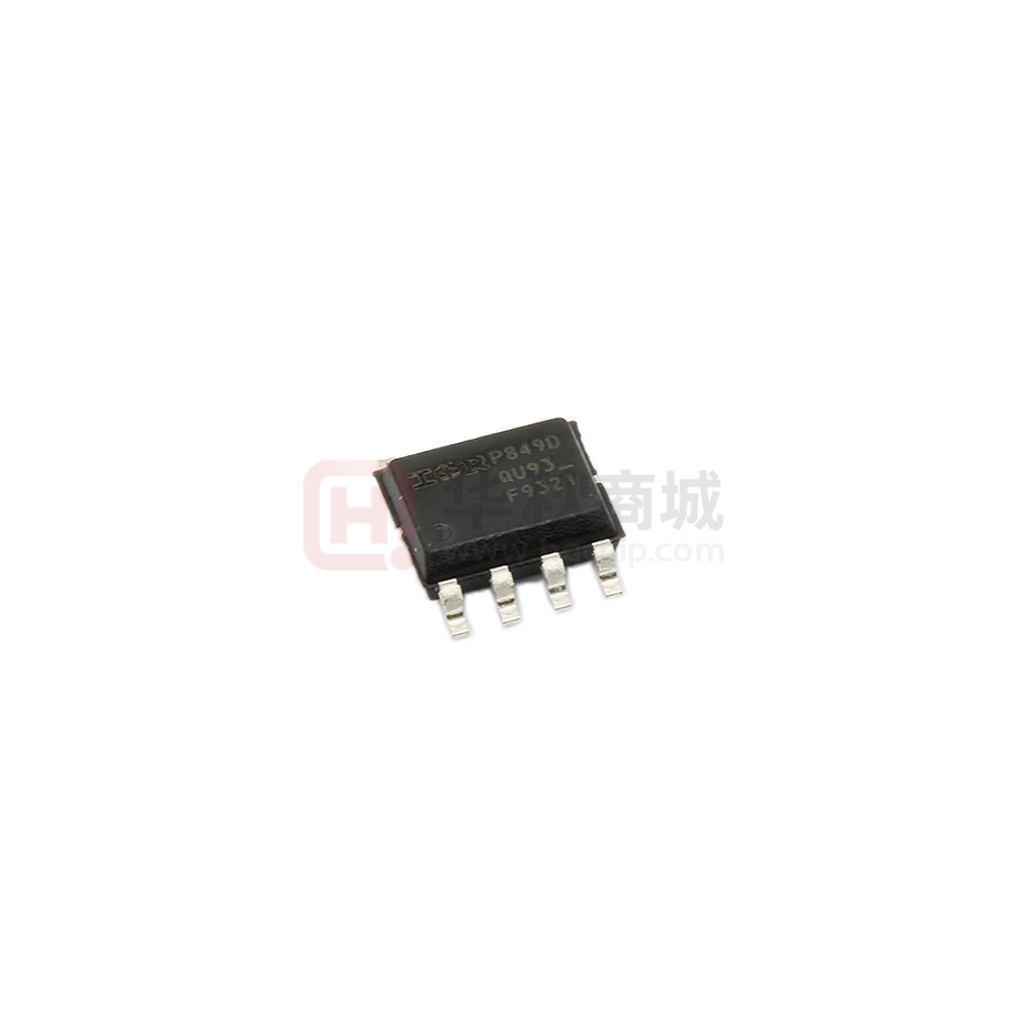
SO-8
Applications
• Charge and Discharge Switch for Notebook PC Battery Application
Features and Benefits
Features
Industry-Standard SO-8 Package
RoHS Compliant Containing no Lead, no Bromide and no Halogen
Orderable part number
Package Type
IRF9321PbF
IRF9321TRPbF
SO8
SO8
Resulting Benefits
results in Multi-Vendor Compatibility
Environmentally Friendlier
⇒
Standard Pack
Form
Quantity
Tube/Bulk
95
Tape and Reel
4000
Note
Absolute Maximum Ratings
Parameter
Max.
VDS
Drain-to-Source Voltage
-30
VGS
Gate-to-Source Voltage
±20
ID @ TA = 25°C
Continuous Drain Current, VGS @ -10V
-15
ID @ TA = 70°C
Continuous Drain Current, VGS @ -10V
-12
Pulsed Drain Current
-120
IDM
PD @TA = 25°C
PD @TA = 70°C
f
Power Dissipation f
c
Power Dissipation
TJ
Linear Derating Factor
Operating Junction and
TSTG
Storage Temperature Range
2.5
1.6
0.02
-55 to + 150
Units
V
A
W
W/°C
°C
Notes through are on page 2
www.irf.com
1
05/11/2010
�IRF9321PbF
Static @ TJ = 25°C (unless otherwise specified)
Min.
Typ.
Max.
Units
BVDSS
Drain-to-Source Breakdown Voltage
Parameter
-30
–––
–––
V
∆ΒVDSS/∆TJ
RDS(on)
Breakdown Voltage Temp. Coefficient
–––
–––
0.021
5.9
–––
7.2
V/°C
–––
9.3
11.2
Static Drain-to-Source On-Resistance
mΩ
VGS(th)
Gate Threshold Voltage
-1.3
-1.8
-2.4
V
∆VGS(th)
IDSS
Gate Threshold Voltage Coefficient
Drain-to-Source Leakage Current
–––
–––
-5.9
–––
–––
-1.0
mV/°C
–––
–––
-150
µA
IGSS
Gate-to-Source Forward Leakage
Gate-to-Source Reverse Leakage
–––
–––
–––
–––
-100
100
nA
gfs
Qg
Forward Transconductance
Total Gate Charge
30
–––
–––
34
–––
–––
S
nC
Qg
Qgs
Gate-to-Source Charge
–––
–––
65
10
98
–––
nC
–––
–––
16
18
–––
–––
Ω
Turn-On Delay Time
Rise Time
–––
–––
21
79
–––
–––
td(off)
Turn-Off Delay Time
–––
185
–––
tf
Ciss
Fall Time
Input Capacitance
–––
–––
145
2590
–––
–––
Coss
Crss
Output Capacitance
Reverse Transfer Capacitance
–––
–––
590
360
–––
–––
Qgd
RG
td(on)
tr
h
Total Gate Charge h
h
Gate-to-Drain Charge h
Gate Resistance h
Conditions
VGS = 0V, ID = -250µA
Reference to 25°C, ID = -1mA
VGS = -10V, ID = -15A
VGS = -4.5V, ID = -12A
e
e
VDS = VGS, ID = -50µA
VDS = -24V, VGS = 0V
VDS = -24V, VGS = 0V, TJ = 125°C
VGS = -20V
VGS = 20V
VDS = -10V, ID = -12A
VDS = -15V, VGS = -4.5V, ID = - 12A
VGS = -10V
VDS = -15V
ID = -12A
ns
VDD = -30V, VGS = -4.5V
ID = -1.0A
e
RG = 6.8Ω
See Figs. 19a & 19b
VGS = 0V
pF
VDS = -25V
ƒ = 1.0MHz
Avalanche Characteristics
Parameter
EAS
IAR
Single Pulse Avalanche Energy
Avalanche Current
c
Diode Characteristics
Parameter
d
Min.
IS
Continuous Source Current
ISM
(Body Diode)
Pulsed Source Current
–––
Typ.
–––
Typ.
Max.
Units
–––
–––
310
-12
mJ
A
Max.
Units
Conditions
MOSFET symbol
-2.5
A
showing the
integral reverse
D
G
(Body Diode)�c
–––
–––
-120
VSD
Diode Forward Voltage
–––
–––
-1.2
V
TJ = 25°C, IS = -2.5A, VGS = 0V
trr
Reverse Recovery Time
–––
38
57
ns
TJ = 25°C, IF = -2.5A, VDD = -24V
Qrr
Reverse Recovery Charge
–––
24
36
nC
di/dt = 100/µs
p-n junction diode.
Thermal Resistance
Parameter
RθJL
Junction-to-Drain Lead
RθJA
Junction-to-Ambient
f
g
Typ.
Max.
–––
20
–––
50
S
e
e
Units
°C/W
Notes:
Repetitive rating; pulse width limited by max. junction temperature.
Starting TJ = 25°C, L = 4.3mH, RG = 25Ω, IAS = -12A.
Pulse width ≤ 400µs; duty cycle ≤ 2%.
When mounted on 1 inch square copper board.
Rθ is measured at TJ of approximately 90°C.
For DESIGN AID ONLY, not subject to production testing.
2
www.irf.com
�IRF9321PbF
1000
1000
100
BOTTOM
10
TOP
-ID, Drain-to-Source Current (A)
-ID, Drain-to-Source Current (A)
TOP
VGS
-10V
-5.0V
-4.5V
-4.0V
-3.5V
-3.0V
-2.8V
-2.5V
100
1
-2.5V
0.1
≤60µs PULSE WIDTH
BOTTOM
10
-2.5V
1
≤60µs PULSE WIDTH
Tj = 150°C
Tj = 25°C
0.01
0.1
0.1
1
10
100
0.1
-V DS, Drain-to-Source Voltage (V)
10
100
Fig 2. Typical Output Characteristics
1000
1.6
RDS(on) , Drain-to-Source On Resistance
(Normalized)
-I D, Drain-to-Source Current (A)
1
-V DS, Drain-to-Source Voltage (V)
Fig 1. Typical Output Characteristics
100
10
T J = 25°C
TJ = 150°C
1
VDS = -10V
≤60µs PULSE WIDTH
0.1
1
2
3
4
ID = -15A
VGS = -10V
1.4
1.2
1.0
0.8
0.6
5
-60 -40 -20 0
Fig 3. Typical Transfer Characteristics
100000
Fig 4. Normalized On-Resistance vs. Temperature
14.0
VGS = 0V,
f = 1 MHZ
C iss = C gs + C gd, C ds SHORTED
C rss = C gd
-V GS, Gate-to-Source Voltage (V)
ID= -12A
C oss = C ds + C gd
10000
Ciss
Coss
Crss
1000
20 40 60 80 100 120 140 160
T J , Junction Temperature (°C)
-V GS, Gate-to-Source Voltage (V)
C, Capacitance (pF)
VGS
-10V
-5.0V
-4.5V
-4.0V
-3.5V
-3.0V
-2.8V
-2.5V
12.0
VDS= -24V
VDS= -15V
10.0
VDS= -6.0V
8.0
6.0
4.0
2.0
0.0
100
1
10
100
-VDS, Drain-to-Source Voltage (V)
Fig 5. Typical Capacitance vs.Drain-to-Source Voltage
www.irf.com
0
25
50
75
100
QG, Total Gate Charge (nC)
Fig 6. Typical Gate Charge vs.Gate-to-Source Voltage
3
�IRF9321PbF
1000
-I D, Drain-to-Source Current (A)
-I SD, Reverse Drain Current (A)
1000
OPERATION IN THIS AREA
LIMITED BY R DS(on)
100µsec
100
100
T J = 150°C
T J = 25°C
10
1msec
10msec
10
DC
1
T A = 25°C
Tj = 150°C
Single Pulse
VGS = 0V
1.0
0.1
0.3
0.5
0.7
0.9
1.1
0.01
1.3
Fig 7. Typical Source-Drain Diode Forward Voltage
1
10
100
Fig 8. Maximum Safe Operating Area
2.4
-V GS(th), Gate threshold Voltage (V)
15
-I D, Drain Current (A)
0.1
-VDS, Drain-to-Source Voltage (V)
-V SD, Source-to-Drain Voltage (V)
10
5
2.2
2.0
1.8
ID = -50µA
1.6
1.4
1.2
1.0
0
25
50
75
100
125
-75 -50 -25
150
0
25
50
75 100 125 150
T J , Temperature ( °C )
T A , Ambient Temperature (°C)
Fig 10. Threshold Voltage vs. Temperature
Fig 9. Maximum Drain Current vs.
Ambient Temperature
Thermal Response ( Z thJA ) °C/W
100
D = 0.50
10
0.20
0.10
0.05
0.02
0.01
1
0.1
0.01
Notes:
1. Duty Factor D = t1/t2
2. Peak Tj = P dm x Zthja + T A
SINGLE PULSE
( THERMAL RESPONSE )
0.001
1E-006
1E-005
0.0001
0.001
0.01
0.1
1
10
100
1000
t1 , Rectangular Pulse Duration (sec)
Fig 11. Maximum Effective Transient Thermal Impedance, Junction-to-Ambient
4
www.irf.com
�IRF9321PbF
RDS(on), Drain-to -Source On Resistance ( mΩ)
RDS(on), Drain-to -Source On Resistance (m Ω)
20
ID = -15A
18
16
14
12
10
T J = 125°C
8
6
4
T J = 25°C
2
0
2
4
6
8
10
12
14
16
18
50
40
Vgs = -4.5V
30
20
Vgs = -10V
10
0
20
0
20
40
60
-V GS, Gate -to -Source Voltage (V)
100
120
Fig 13. Typical On-Resistance vs. Drain Current
1400
1000
ID
TOP
-1.4A
-2.2A
BOTTOM -12A
1000
800
Single Pulse Power (W)
1200
800
600
400
600
400
200
200
0
25
50
75
100
125
0
1E-5
150
1E-4
Starting T J , Junction Temperature (°C)
D.U.T *
1E-2
Driver Gate Drive
+
-
D.U.T. ISD Waveform
Reverse
Recovery
Current
+
di/dt controlled by RG
Driver same type as D.U.T.
I SD controlled by Duty Factor "D"
D.U.T. - Device Under Test
VDD
+
-
Re-Applied
Voltage
Body Diode Forward
Current
di/dt
D.U.T. VDS Waveform
Diode Recovery
dv/dt
Body Diode
www.irf.com
VDD
Forward Drop
Inductor
Current
Inductor Curent
Ripple ≤ 5%
Reverse Polarity of D.U.T for P-Channel
P.W.
Period
*
•
•
•
•
1E+0
VGS=10V
Circuit Layout Considerations
• Low Stray Inductance
• Ground Plane
• Low Leakage Inductance
Current Transformer
-
D=
Period
P.W.
1E-1
Fig 15. Typical Power vs. Time
+
RG
1E-3
Time (sec)
Fig 14. Maximum Avalanche Energy vs. Drain Current
*
80
-I D, Drain Current (A)
Fig 12. On-Resistance vs. Gate Voltage
EAS , Single Pulse Avalanche Energy (mJ)
60
ISD
* VGS = 5V for Logic Level Devices
Fig 16. Diode Reverse Recovery Test Circuit for P-Channel HEXFET® Power MOSFETs
5
�IRF9321PbF
Id
Vds
Vgs
L
VCC
DUT
0
20K
1K
Vgs(th)
SS
Qgodr
Fig 17a. Gate Charge Test Circuit
I AS
D.U.T
RG
IAS
-V
GS
-20V
tp
Qgs2 Qgs1
Fig 17b. Gate Charge Waveform
L
VDS
Qgd
VDD
A
DRIVER
0.01Ω
tp
V(BR)DSS
15V
Fig 18b. Unclamped Inductive Waveforms
Fig 18a. Unclamped Inductive Test Circuit
VDS
RD
td(on)
VGS
RG
t d(off)
tf
VGS
D.U.T.
10%
+
V DD
-VGS
Pulse Width ≤ 1 µs
Duty Factor ≤ 0.1 %
Fig 19a. Switching Time Test Circuit
6
tr
90%
VDS
Fig 19b. Switching Time Waveforms
www.irf.com
�IRF9321PbF
SO-8 Package Outline(Mosfet & Fetky)
Dimensions are shown in milimeters (inches)
'
,1&+(6
0,1
0$;
$ ����� �����
$� ����� �����
E ����
����
F
����� �����
' ����
�����
( ����� �����
H
������%$6,&
H � ������%$6,&
+ ����� �����
. ����� �����
/ ����
����
\
��
��
',0
%
�
$
�
�
�
�
�
�
�
�
�
+
�����>����@�
(
$
�; H
H�
�;�E
�����>����@�
$
.�[���
&
\
�����>����@�
$�
0,//,0(7(56
0,1
0$;
����
����
����
����
����
����
����
����
����
����
����
����
������%$6,&
�������%$6,&
����
����
����
����
����
����
��
��
�;�/
�;�F
�
& $ %
)22735,17
127(6�
����',0(16,21,1*� �72/(5$1&,1*�3(5�$60(�,1&+(6@�
����287/,1(�&21)2506�72�-('(&�287/,1(�06����$$�
����',0(16,21�'2(6�127�,1&/8'(�02/'�3527586,216�
�����02/'�3527586,216�127�72�(;&(('������>����@�
����',0(16,21�'2(6�127�,1&/8'(�02/'�3527586,216�
�����02/'�3527586,216�127�72�(;&(('������>����@�
����',0(16,21�,6�7+(�/(1*7+�2)�/($'�)25�62/'(5,1*�72
�����$�68%675$7(�
�;������>����@
�����>����@
�;������>����@
�;������>����@
SO-8 Part Marking Information
(;$03/(��7+,6�,6�$1�,5)������026)(7�
,17(51$7,21$/
5(&7,),(5
/2*2
;;;;
)����
'$7(�&2'(��


 工商网监
湘ICP备2023018690号
工商网监
湘ICP备2023018690号
