IRFL4105PbF
Surface Mount
Advanced Process Technology
Ultra Low On-Resistance
Dynamic dv/dt Rating
Fast Switching
Fully Avalanche Rated
Lead-Free
HEXFET® Power MOSFET
Description
Fifth Generation HEXFETs from International Rectifier utilize
advanced processing techniques to achieve extremely low onresistance per silicon area. This benefit, combined with the fast
switching speed and ruggedized device design that HEXFET
Power MOSFETs are well known for, provides the designer with
an extremely efficient and reliable device for use in a wide variety
of applications.
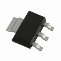
The SOT-223 package is designed for surface-mount using vapor
phase, infra red, or wave soldering techniques. Its unique
package design allows for easy automatic pick-and-place as with
other SOT or SOIC packages but has the added advantage of
improved thermal performance due to an enlarged tab for heat
sinking. Power dissipation of 1.0W is possible in a typical surface
mount application.
Base Part Number
Package Type
IRFL4105PbF
SOT-223
Absolute Maximum Ratings
Symbol
VDSS
55V
RDS(on)
0.045
ID
3.7A
SOT-223
G
Gate
D
Drain
Standard Pack
Form
Quantity
Tape and Reel
2500
Parameter
Orderable Part Number
IRFL4105PbF
Max.
ID @ TA = 25°C
Continuous Drain Current, VGS @ 10V
5.2
ID @ TA = 25°C
ID @ TA = 70°C
IDM
PD @TA = 25°C
Continuous Drain Current, VGS @ 10V
Continuous Drain Current, VGS @ 10V
Pulsed Drain Current
Maximum Power Dissipation (PCB Mount)
3.7
3.0
30
2.1
PD @TA = 25°C
Maximum Power Dissipation (PCB Mount)
Linear Derating Factor (PCB Mount)
Gate-to-Source Voltage
Single Pulse Avalanche Energy (Thermally Limited)
Avalanche Current
Repetitive Avalanche Energy
Peak Diode Recovery dv/dt
Operating Junction and
Storage Temperature Range
VGS
EAS
IAR
EAR
dv/dt
TJ
TSTG
Thermal Resistance
Symbol
RJA
RJA
1
Parameter
Junction-to-Ambient (PCB Mount, steady state)
Junction-to-Ambient (PCB Mount, steady state)
S
Source
Units
A
1.0
8.3
± 20
110
3.7
0.10
5.0
-55 to + 150
W
mW/°C
V
mJ
A
mJ
V/ns
°C
Typ.
Max.
Units
90
50
120
60
°C/W
2016-5-27
�IRFL4105PbF
Electrical Characteristics @ TJ = 25°C (unless otherwise specified)
V(BR)DSS
V(BR)DSS/TJ
RDS(on)
VGS(th)
gfs
Parameter
Drain-to-Source Breakdown Voltage
Breakdown Voltage Temp. Coefficient
Static Drain-to-Source On-Resistance
Gate Threshold Voltage
Forward Trans conductance
IDSS
Drain-to-Source Leakage Current
Gate-to-Source Forward Leakage
Gate-to-Source Reverse Leakage
Total Gate Charge
Qg
Qgs
Gate-to-Source Charge
Qgd
Gate-to-Drain Charge
td(on)
Turn-On Delay Time
Rise Time
tr
td(off)
Turn-Off Delay Time
Fall Time
tf
Ciss
Input Capacitance
Coss
Output Capacitance
Crss
Reverse Transfer Capacitance
Source-Drain Ratings and Characteristics
Parameter
Continuous Source Current
IS
(Body Diode)
Pulsed Source Current
ISM
(Body Diode)
VSD
Diode Forward Voltage
IGSS
Min. Typ. Max. Units
Conditions
55
–––
–––
V VGS = 0V, ID = 250µA
––– 0.058 ––– V/°C Reference to 25°C, ID = 1mA
––– ––– 0.045
VGS = 10V, ID = 3.7A
2.0
–––
4.0
V VDS = VGS, ID = 250µA
3.8
–––
–––
S VDS = 25V, ID = 1.9A
––– –––
25
VDS = 55 V, VGS = 0V
µA
––– –––
250
VDS = 44V,VGS = 0V,TJ =150°C
––– –––
100
VGS = 20V
nA
––– ––– -100
VGS = -20V
–––
23
35
ID = 3.7A
nC VDS = 44V
–––
3.4
5.1
VGS = 10V , See Fig. 6 and 13
–––
9.8
15
–––
7.1
–––
VDD = 28V
–––
12
–––
ID = 3.7A
ns
–––
19
–––
RG= 6.0
–––
12
–––
RD= 7.5See Fig. 10
––– 660
–––
VGS = 0V
pF VDS = 25V
––– 230
–––
ƒ = 1.0MHz, See Fig. 5
–––
99
–––
Min.
Typ.
Max. Units
–––
–––
1.3
–––
–––
30
–––
–––
1.3
V
Conditions
MOSFET symbol
showing the
integral reverse
p-n junction diode.
TJ = 25°C,IS = 3.7A,VGS = 0V
A
trr
Reverse Recovery Time
–––
55
82
ns
TJ = 25°C ,IF = 3.7A
Qrr
Reverse Recovery Charge
–––
120
170
nC
di/dt = 100A/µs
Notes:
Repetitive rating; pulse width limited by max. junction temperature. (See fig. 11)
starting TJ = 25°C, L = 16mH, RG = 25, IAS = 3.7A (See fig. 12)
ISD 3.7A, di/dt 110A/µs, VDD V(BR)DSS, TJ 150°C.
Pulse width 300µs; duty cycle 2%.
2
2016-5-27
�IRFL4105PbF
100
100
VGS
15V
10V
8.0V
7.0V
6.0V
5.5V
5.0V
BOTTOM 4.5V
I , Drain-to-Source Current (A)
D
I , Drain-to-Source Current (A)
D
10
4.5V
20µs PULSE WIDTH
TC = 25°C
1
0.1
VGS
15V
10V
8.0V
7.0V
6.0V
5.5V
5.0V
BOTTOM 4.5V
TOP
TOP
1
10
A
10
4.5V
20µs PULSE WIDTH
TJ = 150°C
1
0.1
100
1
Fig. 2 Typical Output Characteristics
Fig. 1 Typical Output Characteristics
2.0
TJ = 25°C
TJ = 150°C
10
VDS = 25V
20µs PULSE WIDTH
4.5
5.0
5.5
6.0
6.5
VGS , Gate-to-Source Voltage (V)
Fig. 3 Typical Transfer Characteristics
3
R DS(on) , Drain-to-Source On Resistance
(Normalized)
I D , Drain-to-Source Current (A)
100
4.0
A
100
VDS , Drain-to-Source Voltage (V)
VDS , Drain-to-Source Voltage (V)
1
10
A
7.0
I D = 3.7A
1.5
1.0
0.5
VGS = 10V
0.0
-60
-40
-20
0
20
40
60
80
A
100 120 140 160
TJ , Junction Temperature (°C)
Fig. 4 Normalized On-Resistance
vs. Temperature
2016-5-27
�IRFL4105PbF
C, Capacitance (pF)
1000
Ciss
20
V GS = 0V,
f = 1MHz
C iss = Cgs + C gd , Cds SHORTED
C rss = C gd
C oss = Cds + C gd
V GS , Gate-to-Source Voltage (V)
1200
800
Coss
600
400
Crss
200
0
1
10
100
A
I D = 3.7A
16
12
8
4
FOR TEST CIRCUIT
SEE FIGURE 9
0
0
VDS , Drain-to-Source Voltage (V)
20
30
A
40
Fig 6. Typical Gate Charge vs.
Gate-to-Source Voltage
100
100
OPERATION IN THIS AREA LIMITED
BY RDS(on)
10µs
I D , Drain Current (A)
ISD , Reverse Drain Current (A)
10
Q G , Total Gate Charge (nC)
Fig 5. Typical Capacitance vs.
Drain-to-Source Voltage
TJ = 150°C
10
TJ = 25°C
VGS = 0V
1
0.4
0.6
0.8
1.0
1.2
1.4
VSD , Source-to-Drain Voltage (V)
Fig. 7 Typical Source-to-Drain Diode
Forward Voltage
4
VDS = 24V
VDS = 15V
A
1.6
10
100µs
1ms
1
10ms
TA = 25°C
TJ = 150°C
Single Pulse
0.1
0.1
1
A
10
100
VDS , Drain-to-Source Voltage (V)
Fig 8. Maximum Safe Operating Area
2016-5-27
�IRFL4105PbF
Fig 10a. Switching Time Test Circuit
Fig 9a. Basic Gate Charge Waveform
Fig 10b. Switching Time Waveforms
Fig 9b. Gate Charge Test Circuit
Thermal Response (ZthJA )
1000
100
D = 0.50
0.20
10
0.10
0.05
0.02
1
0.01
PDM
t
0.1
0.01
0.00001
SINGLE PULSE
(THERMAL RESPONSE)
Notes:
1. Duty factor D = t
1
t
2
1
/t
2
2. Peak TJ = PDM x Z thJA + T
A
0.0001
0.001
0.01
0.1
1
10
100
1000
A
10000
t 1 , Rectangular Pulse Duration (sec)
Fig 11. Maximum Effective Transient Thermal Impedance, Junction-to-Ambient
5
2016-5-27
�IRFL4105PbF
15V
L
VDS
DRIVER
D.U.T
RG
+
V
- DD
IAS
20V
tp
A
0.01
Fig 12a. Unclamped Inductive Test Circuit
EAS , Single Pulse Avalanche Energy (mJ)
300
TOP
250
BOTTOM
200
150
100
50
0
VDD = 25V
25
V(BR)DSS
tp
ID
1.7A
3.0A
3.7A
50
75
100
A
125
150
Starting TJ , Junction Temperature (°C)
Fig 12c. Maximum Avalanche Energy
vs. Drain Current
I AS
Fig 12b. Unclamped Inductive Waveforms
6
2016-5-27
�IRFL4105PbF
Fig 13. Peak Diode Recovery dv/dt Test Circuit for N-Channel HEXFET® Power MOSFETs
7
2016-5-27
�IRFL4105PbF
SOT-223 (TO-261AA) Package Outline (Dimensions are shown in millimeters (inches)
SOT-223(TO-261AA) Part Marking Information
FL014N
Date Code
Y= Year
WW= Work Week
A= Automotive, Lead Free
Note: For the most current drawing please refer to Infineon’s web site www.infineon.com
8
2016-5-27
�IRFL4105PbF
SOT-223(TO-261AA) Tape and Reel (Dimensions are shown in millimeters (inches)
2.05 (.080)
1.95 (.077)
TR
4.10 (.161)
3.90 (.154)
0.35 (.013)
0.25 (.010)
1.85 (.072)
1.65 (.065)
7.55 (.297)
7.45 (.294)
16.30 (.641)
15.70 (.619)
7.60 (.299)
7.40 (.292)
1.60 (.062)
1.50 (.059)
TYP.
FEED DIRECTION
12.10 (.475)
11.90 (.469)
2.30 (.090)
2.10 (.083)
7.10 (.279)
6.90 (.272)
NOTES :
1. CONTROLLING DIMENSION: MILLIMETER.
2. OUTLINE CONFORMS TO EIA-481 & EIA-541.
3. EACH O330.00 (13.00) REEL CONTAINS 2,500 DEVICES.
13.20 (.519)
12.80 (.504)
15.40 (.607)
11.90 (.469)
4
330.00
(13.000)
MAX.
NOTES :
1. OUTLINE COMFORMS TO EIA-418-1.
2. CONTROLLING DIMENSION: MILLIMETER..
3. DIMENSION MEASURED @ HUB.
4. INCLUDES FLANGE DISTORTION @ OUTER EDGE.
50.00 (1.969)
MIN.
18.40 (.724)
MAX.
14.40 (.566)
12.40 (.488)
4
3
Note: For the most current drawing please refer to Infineon’s web site www.infineon.com
9
2016-5-27
�IRFL4105PbF
Qualification Information†
Qualification Level
Moisture Sensitivity Level
SOT-223
RoHS Compliant
Industrial
(per JEDEC JESD47F) ††
MSL1
(per JEDEC J-STD-020D) ††
Yes
†
Qualification standards can be found at Infineon’s web site www.infineon.com
††
Applicable version of JEDEC standard at the time of product release.
Revision History
Date
5/27/2016
Comments
Updated datasheet with corporate template.
Added disclaimer on last page.
Trademarks of Infineon Technologies AG
µHVIC™, µIPM™, µPFC™, AU‐ConvertIR™, AURIX™, C166™, CanPAK™, CIPOS™, CIPURSE™, CoolDP™, CoolGaN™, COOLiR™, CoolMOS™, CoolSET™, CoolSiC™,
DAVE™, DI‐POL™, DirectFET™, DrBlade™, EasyPIM™, EconoBRIDGE™, EconoDUAL™, EconoPACK™, EconoPIM™, EiceDRIVER™, eupec™, FCOS™, GaNpowIR™,
HEXFET™, HITFET™, HybridPACK™, iMOTION™, IRAM™, ISOFACE™, IsoPACK™, LEDrivIR™, LITIX™, MIPAQ™, ModSTACK™, my‐d™, NovalithIC™, OPTIGA™,
Op MOS™, ORIGA™, PowIRaudio™, PowIRStage™, PrimePACK™, PrimeSTACK™, PROFET™, PRO‐SIL™, RASIC™, REAL3™, SmartLEWIS™, SOLID FLASH™,
SPOC™, StrongIRFET™, SupIRBuck™, TEMPFET™, TRENCHSTOP™, TriCore™, UHVIC™, XHP™, XMC™
Trademarks updated November 2015
Other Trademarks
All referenced product or service names and trademarks are the property of their respec ve owners.
Edi on 2016‐04‐19
Published by
Infineon Technologies AG
81726 Munich, Germany
© 2016 Infineon Technologies AG.
All Rights Reserved.
Do you have a ques on about this
document?
Email: erratum@infineon.com
Document reference
ifx1
10
IMPORTANT NOTICE
The informa on given in this document shall in no
event be regarded as a guarantee of condi ons or
characteris cs (“Beschaffenheitsgaran e”) .
With respect to any examples, hints or any typical
values stated herein and/or any informa on
regarding the applica on of the product, Infineon
Technologies hereby disclaims any and all
warran es and liabili es of any kind, including
without limita on warran es of non‐infringement
of intellectual property rights of any third party.
In addi on, any informa on given in this document
is subject to customer’s compliance with its
obliga ons stated in this document and any
applicable legal requirements, norms and
standards concerning customer’s products and any
use of the product of Infineon Technologies in
customer’s applica ons.
The data contained in this document is exclusively
intended for technically trained staff. It is the
responsibility of customer’s technical departments
to evaluate the suitability of the product for the
intended applica on and the completeness of the
product informa on given in this document with
respect to such applica on.
For further informa on on the product, technology,
delivery terms and condi ons and prices please
contact your nearest Infineon Technologies office
(www.infineon.com).
Please note that this product is not qualified
according to the AEC Q100 or AEC Q101 documents
of the Automo ve Electronics Council.
WARNINGS
Due to technical requirements products may
contain dangerous substances. For informa on on
the types in ques on please contact your nearest
Infineon Technologies office.
Except as otherwise explicitly approved by Infineon
Technologies in a wri en document signed by
authorized representa ves of Infineon Technologies,
Infineon Technologies’ products may not be used in
any applica ons where a failure of the product or
any consequences of the use thereof can reasonably
be expected to result in personal injury.
2016-5-27
�