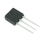
IRFR3707ZPbF
IRFU3707ZPbF
HEXFET® Power MOSFET
Applications
High Frequency Synchronous Buck
Converters for Computer Processor Power
High Frequency Isolated DC-DC
Converters with Synchronous Rectification
for Telecom and Industrial Use
VDSS
30V
RDS(on) max
9.5m
Qg
9.6nC
D
D
S
G
Package Type
IRFU3707ZPbF
I-Pak
IRFR3707ZPbF
D-Pak
Absolute Maximum Ratings
Symbol
I- Pak
IRFU3707ZPbF
D- Pak
IRFR3707ZPbF
Benefits
Very Low RDS(on) at 4.5V VGS
Ultra - Low Gate Impedance
Fully Characterized Avalanche Voltage and Current
Lead-Free
Base part number
G
G
Gate
D
Drain
Standard Pack
S
D
S
Source
Orderable Part Number
Form
Quantity
Tube
75
IRFU3707ZPbF
Tube
75
IRFR3707ZPbF
Tape and Reel Left
3000
IRFR3707ZTRLPbF
Max.
Units
VDS
Drain -to-Source Voltage
Parameter
30
V
VGS
Gate-to-Source Voltage
± 20
V
ID @ TC = 25°C
Continuous Drain Current, VGS @ 10V
56
ID @ TC = 100°C
IDM
PD @TC = 25°C
Continuous Drain Current, VGS @ 10V
Pulsed Drain Current
Maximum Power Dissipation
39
220
50
PD @TC = 100°C
Maximum Power Dissipation
TJ
TSTG
Linear Derating Factor
Operating Junction and
Storage Temperature Range
Soldering Temperature, for 10 seconds (1.6mm from case)
Thermal Resistance
Symbol
Parameter
Junction-to-Case
RJC
Junction-to-Ambient ( PCB Mount)
RJA
Junction-to-Ambient
RJA
A
W
25
W
0.33
-55 to + 175
W/°C
300
°C
Typ.
–––
–––
–––
Max.
3.0
50
110
Units
°C/W
Notes through are on page 2.
1
2016-5-31
�IRFR/U3707ZPbF
Static @ TJ = 25°C (unless otherwise specified)
V(BR)DSS
V(BR)DSS/TJ
Parameter
Drain-to-Source Breakdown Voltage
Breakdown Voltage Temp. Coefficient
RDS(on)
Static Drain-to-Source On-Resistance
VGS(th)
Gate Threshold Voltage
VGS(th)/TJ
Gate Threshold Voltage Temp. Coefficient
IDSS
Drain-to-Source Leakage Current
IGSS
gfs
Qg
Qgs1
Qgs2
Qgd
Qgodr
Qsw
Qoss
td(on)
tr
td(off)
tf
Ciss
Coss
Crss
Gate-to-Source Forward Leakage
Gate-to-Source Reverse Leakage
Forward Trans conductance
Total Gate Charge
Pre-Vth Gate-to-Source Charge
Post-Vth Gate-to-Source Charge
Gate-to-Drain Charge
Gate Charge Overdrive
Switch Charge (Qgs2 + Qgd)
Output Charge
Turn-On Delay Time
Rise Time
Turn-Off Delay Time
Fall Time
Input Capacitance
Output Capacitance
Reverse Transfer Capacitance
Min. Typ. Max. Units
Conditions
30
–––
–––
V VGS = 0V, ID = 250µA
––– 0.023 ––– V/°C Reference to 25°C, ID = 1mA
–––
7.5
9.5
VGS = 10V, ID = 15A
m
–––
10
12.5
VGS = 4.5V, ID = 12A
1.35 1.80 2.25
V
VDS = VGS, ID = 25µA
––– -5.0 ––– mV/°C
–––
–––
–––
–––
71
–––
–––
–––
–––
–––
–––
–––
–––
–––
–––
–––
–––
–––
–––
–––
–––
–––
–––
9.6
2.6
0.90
3.5
2.6
4.4
5.8
8.0
11
12
3.3
1150
260
120
1.0
150
100
-100
–––
14
–––
–––
–––
–––
–––
–––
–––
–––
–––
–––
–––
–––
–––
µA
nA
S
VDS = 24V, VGS = 0V
VDS = 24V,VGS = 0V,TJ =125°C
VGS = 20V
VGS = -20V
VDS = 15V, ID = 12A
VDS = 15V
V = 4.5V
nC GS
ID = 12A
See Fig. 16
nC VDS = 15V, VGS = 0V
VDD = 16V,VGS = 4.5V
ID = 12A
ns
Clamped Inductive Load
VGS = 0V
pF VDS = 15V
ƒ = 1.0MHz
Avalanche Characteristics
Parameter
Single Pulse Avalanche Energy
Avalanche Current
Repetitive Avalanche Energy
EAS
IAR
EAR
Max.
Units
42
12
5.0
mJ
A
mJ
Diode Characteristics
Parameter
Continuous Source Current
(Body Diode)
Pulsed Source Current
(Body Diode)
Diode Forward Voltage
Reverse Recovery Time
Reverse Recovery Charge
Forward Turn-On Time
IS
ISM
VSD
trr
Qrr
ton
Min.
Typ.
Max. Units
–––
–––
56
A
–––
–––
220
–––
–––
–––
–––
25
17
1.0
38
26
V
ns
nC
Conditions
MOSFET symbol
showing the
integral reverse
p-n junction diode.
TJ = 25°C,IS = 12A,VGS = 0V
TJ = 25°C ,IF = 12A, VDS = 15V
di/dt = 100A/µs
Intrinsic turn-on time is negligible (turn-on is dominated by LS+LD)
Notes:
Repetitive rating; pulse width limited by max. junction temperature
starting TJ = 25°C, L = 0.58mH, RG = 25, IAS = 12A.
Pulse width 400µs; duty cycle 2%.
Calculated continuous current based on maximum allowable junction temperature. Package limitation current is 30A.
When mounted on 1" square PCB (FR-4 or G-10 Material). For recommended footprint and soldering techniques refer to
application note #AN-994.
2
2016-5-31
�IRFR/U3707ZPbF
1000
10000
ID, Drain-to-Source Current (A)
1000
100
BOTTOM
TOP
ID, Drain-to-Source Current (A)
TOP
VGS
10V
6.0V
4.5V
4.0V
3.3V
2.8V
2.5V
2.2V
10
1
0.1
2.2V
0.01
10
2.2V
1
0.1
0.001
1
BOTTOM
20µs PULSE WIDTH
Tj = 175°C
20µs PULSE WIDTH
Tj = 25°C
0.1
100
0.1
10
10
Fig. 2 Typical Output Characteristics
Fig. 1 Typical Output Characteristics
2.0
100
RDS(on) , Drain-to-Source On Resistance
(Normalized)
1000
ID, Drain-to-Source Current )
1
VDS , Drain-to-Source Voltage (V)
VDS, Drain-to-Source Voltage (V)
T J = 175°C
10
1
T J = 25°C
0.1
VDS = 10V
20µs PULSE WIDTH
0
2
4
6
VGS, Gate-to-Source Voltage (V)
Fig. 3 Typical Transfer Characteristics
ID = 30A
VGS = 10V
1.5
1.0
0.5
0.01
3
VGS
10V
6.0V
4.5V
4.0V
3.3V
2.8V
2.5V
2.2V
8
-60 -40 -20 0
20 40 60 80 100 120 140 160 180
T J , Junction Temperature (°C)
Fig. 4 Normalized On-Resistance
vs. Temperature
2016-5-31
�IRFR/U3707ZPbF
6.0
10000
VGS = 0V,
f = 1 MHZ
Ciss = C gs + Cgd, C ds SHORTED
Crss = C gd
ID= 12A
VGS, Gate-to-Source Voltage (V)
C, Capacitance(pF)
Coss = Cds + Cgd
Ciss
1000
Coss
VDS = 24V
VDS = 15V
5.0
4.0
3.0
2.0
1.0
Crss
0.0
100
1
10
0
100
2
4
6
8
10
12
QG Total Gate Charge (nC)
VDS , Drain-to-Source Voltage (V)
Fig 6. Typical Gate Charge vs.
Gate-to-Source Voltage
Fig 5. Typical Capacitance vs.
Drain-to-Source Voltage
1000.00
1000
ID, Drain-to-Source Current (A)
ISD, Reverse Drain Current (A)
OPERATION IN THIS AREA
LIMITED BY R DS (on)
100.00
100
T J = 175°C
10.00
1.00
T J = 25°C
100µsec
1msec
1
10msec
Tc = 25°C
Tj = 175°C
Single Pulse
VGS = 0V
0.10
0.1
0.2 0.4 0.6 0.8 1.0 1.2 1.4 1.6 1.8 2.0 2.2
VSD , Source-to-Drain Voltage (V)
Fig. 7 Typical Source-to-Drain Diode
Forward Voltage
4
10
0
1
10
100
1000
VDS , Drain-to-Source Voltage (V)
Fig 8. Maximum Safe Operating Area
2016-5-31
�IRFR/U3707ZPbF
60
Limited By Package
50
ID, Drain Current (A)
VGS(th) Gate threshold Voltage (V)
2.5
40
30
20
10
0
2.0
ID = 250µA
1.5
1.0
25
50
75
100
125
150
-75 -50 -25
175
TC , Case Temperature (°C)
0
25
50
75 100 125 150 175 200
T J , Temperature ( °C )
Fig 9. Maximum Drain Current vs. Case Temperature
Fig 10. Threshold Voltage vs. Temperature
Thermal Response ( Z thJC )
10
1
D = 0.50
0.20
0.10
0.1
0.01
0.05
0.02
0.01
J
SINGLE PULSE
( THERMAL RESPONSE )
R1
R1
J
1
R2
R2
R3
R3
C
1
2
2
3
Ci= iRi
Ci= iRi
3
C
Ri (°C/W)
i (sec)
0.823
0.000128
1.698
0.000845
0.481
0.016503
Notes:
1. Duty Factor D = t1/t2
2. Peak Tj = P dm x Zthjc + Tc
0.001
1E-006
1E-005
0.0001
0.001
0.01
0.1
t1 , Rectangular Pulse Duration (sec)
Fig 11. Maximum Effective Transient Thermal Impedance, Junction-to-Case
5
2016-5-31
�IRFR/U3707ZPbF
200
DRIVER
L
VDS
D.U.T
RG
+
V
- DD
IAS
20V
A
0.01
tp
Fig 12a. Unclamped Inductive Test Circuit
V(BR)DSS
tp
EAS , Single Pulse Avalanche Energy (mJ)
15V
ID
TOP
3.7A
5.6A
BOTTOM 12A
180
160
140
120
100
80
60
40
20
0
25
50
75
100
125
150
175
Starting T J , Junction Temperature (°C)
Fig 12c. Maximum Avalanche Energy
vs. Drain Current
I AS
Fig 12b. Unclamped Inductive Waveforms
LD
VDS
Id
Vds
+
Vgs
VDD D.U.T
Vgs(th)
VGS
Pulse Width < 1µs
Duty Factor < 0.1%
Qgs1 Qgs2
Qgd
Qgodr
Fig 14a. Switching Time Test Circuit
Fig 13a. Gate Charge Waveform
VDS
90%
10%
VGS
td(on)
Fig 13b. Gate Charge Test Circuit
6
tr
td(off)
tf
Fig 14b. Switching Time Waveforms
2016-5-31
�IRFR/U3707ZPbF
Fig 15. Peak Diode Recovery dv/dt Test Circuit for N-Channel HEXFET® Power MOSFETs
7
2016-5-31
�IRFR/U3707ZPbF
Power MOSFET Selection for Non-Isolated DC/DC Converters
Control FET
Synchronous FET
Special attention has been given to the power losses in
the switching elements of the circuit - Q1 and Q2. Power
losses in the high side switch Q1, also called the Control
FET, are impacted by the Rds(on) of the MOSFET, but
these conduction losses are only about one half of the
total losses.
The power loss equation for Q2 is approximated by;
Power losses in the control switch Q1 are given by;
Ploss = Pconduction+ Pswitching+ Pdrive+ Poutput
This can be expanded and approximated by;
Ploss Irms Rds(on)
2
Q
Q
I gd Vin f I gs2 Vin f
i
i
g
g
Qg Vg f
Qoss
Vin f
2
This simplified loss equation includes the terms Qgs2 and
Qoss which are new to Power MOSFET data sheets.
Qgs2 is a subelement of traditional gate-source charge
that is included in all MOSFET data sheets. The importance of
splitting this gate-source charge into two sub elements,
Qgs1 and Qgs2, can be seen from Fig 16.
Qgs2 indicates the charge that must be supplied by the
gate driver between the time that the threshold voltage
has been reached and the time the drain current rises to
Id max at which time the drain voltage begins to change.
Minimizing Qgs2 is a critical factor in reducing switching
losses in Q1.
Qoss is the charge that must be supplied to the output
capacitance of the MOSFET during every switching cycle.
Figure A shows how Qoss is formed by the parallel combination
of the voltage dependent (non-linear) capacitance’s Cds
and Cdg when multiplied by the power supply input buss
voltage.
*
Ploss Pconduction Pdrive Poutput
2
Ploss Irms Rds(on)
Qg Vg f
Q
oss Vin f Qrr Vin f
2
*dissipated primarily in Q1
For the synchronous MOSFET Q2, Rds(on) is an important
characteristic; however, once again the importance of
gate charge must not be overlooked since it impacts
three critical areas. Under light load the MOSFET must
still be turned on and off by the control IC so the gate
drive losses become much more significant. Secondly,
the output charge Qoss and reverse recovery charge Qrr
both generate losses that are transferred to Q1 and increase the dissipation in that device. Thirdly, gate charge
will impact the MOSFETs’ susceptibility to Cdv/dt turn on.
The drain of Q2 is connected to the switching node of the
converter and therefore sees transitions between ground
and Vin. As Q1 turns on and off there is a rate of change
of drain voltage dV/dt which is capacitive coupled to the
gate of Q2 and can induce a voltage spike on the gate
that is sufficient to turn the MOSFET on, resulting in
shoot-through current . The ratio of Qgd/Qgs1 must be minimized to reduce the potential for Cdv/dt turn on.
Figure A: Qoss Characteristic
8
2016-5-31
�IRFR/U3707ZPbF
D-Pak (TO-252AA) Package Outline (Dimensions are shown in millimeters (inches))
D-Pak (TO-252AA) Part Marking Information
EXAMPLE: THIS IS AN IRFR120
WITH ASSEMBLY
LOT CODE 1234
ASSEMBLED ON WW 16, 2001
IN THE ASSEMBLY LINE "A"
PART NUMBER
INTERNATIONAL
RECTIFIER
LOGO
Note: "P" in assembly line position
indicates "Lead-Free"
IRFR120
12
116A
34
ASSEMBLY
LOT CODE
DATE CODE
YEAR 1 = 2001
WEEK 16
LINE A
"P" in assembly line position indicates
"Lead-Free" qualification to the consumer-level
OR
INTERNATIONAL
RECTIFIER
LOGO
PART NUMBER
IRFR120
12
ASSEMBLY
LOT CODE
34
DATE CODE
P = DESIGNATES LEAD-FREE
PRODUCT (OPTIONAL)
P = DESIGNATES LEAD-FREE
PRODUCT QUALIFIED TO THE
CONSUMER LEVEL (OPTIONAL)
YEAR 1 = 2001
WEEK 16
A = ASSEMBLY SITE CODE
Note: For the most current drawing please refer to Infineon’s web site www.infineon.com
9
2016-5-31
�IRFR/U3707ZPbF
I-Pak (TO-251AA) Package Outline Dimensions are shown in millimeters (inches)
I-Pak (TO-251AA) Part Marking Information
EXAMPLE: THIS IS AN IRFU120
WITH ASSEMBLY
LOT CODE 5678
ASSEMBLED ON WW 19, 2001
IN THE ASSEMBLY LINE "A"
INTERNATIONAL
RECTIFIER
LOGO
PART NUMBER
IRFU120
119A
56
78
ASSEMBLY
LOT CODE
Note: "P" in assembly line position
indicates Lead-Free"
DATE CODE
YEAR 1 = 2001
WEEK 19
LINE A
OR
INTERNATIONAL
RECTIFIER
LOGO
PART NUMBER
IRFU120
56
ASSEMBLY
LOT CODE
78
DATE CODE
P = DESIGNATES LEAD-FREE
PRODUCT (OPTIONAL)
YEAR 1 = 2001
WEEK 19
A = ASSEMBLY SITE CODE
Note: For the most current drawing please refer to Infineon’s web site www.infineon.com
10
2016-5-31
�IRFR/U3707ZPbF
D-Pak (TO-252AA) Tape & Reel Information Dimensions are shown in millimeters (inches)
TR
TRR
16.3 ( .641 )
15.7 ( .619 )
12.1 ( .476 )
11.9 ( .469 )
FEED DIRECTION
TRL
16.3 ( .641 )
15.7 ( .619 )
8.1 ( .318 )
7.9 ( .312 )
FEED DIRECTION
NOTES :
1. CONTROLLING DIMENSION : MILLIMETER.
2. ALL DIMENSIONS ARE SHOWN IN MILLIMETERS ( INCHES ).
3. OUTLINE CONFORMS TO EIA-481 & EIA-541.
13 INCH
16 mm
NOTES :
1. OUTLINE CONFORMS TO EIA-481.
Note: For the most current drawing please refer to Infineon’s web site www.infineon.com
11
2016-5-31
�IRFR/U3707ZPbF
Qualification Information†
Industrial
(per JEDEC JESD47F) ††
Qualification Level
Moisture Sensitivity Level
D-Pak
MSL1
I-Pak
(per JEDEC J-STD-020D) ††
Yes
RoHS Compliant
†
Qualification standards can be found at Infineon’s web site www.infineon.com
††
Applicable version of JEDEC standard at the time of product release.
Revision History
Date
5/31/2016
Comments
Updated datasheet with corporate template.
Added disclaimer on last page.
Trademarks of Infineon Technologies AG
µHVIC™, µIPM™, µPFC™, AU‐ConvertIR™, AURIX™, C166™, CanPAK™, CIPOS™, CIPURSE™, CoolDP™, CoolGaN™, COOLiR™, CoolMOS™, CoolSET™, CoolSiC™,
DAVE™, DI‐POL™, DirectFET™, DrBlade™, EasyPIM™, EconoBRIDGE™, EconoDUAL™, EconoPACK™, EconoPIM™, EiceDRIVER™, eupec™, FCOS™, GaNpowIR™,
HEXFET™, HITFET™, HybridPACK™, iMOTION™, IRAM™, ISOFACE™, IsoPACK™, LEDrivIR™, LITIX™, MIPAQ™, ModSTACK™, my‐d™, NovalithIC™, OPTIGA™,
Op MOS™, ORIGA™, PowIRaudio™, PowIRStage™, PrimePACK™, PrimeSTACK™, PROFET™, PRO‐SIL™, RASIC™, REAL3™, SmartLEWIS™, SOLID FLASH™,
SPOC™, StrongIRFET™, SupIRBuck™, TEMPFET™, TRENCHSTOP™, TriCore™, UHVIC™, XHP™, XMC™
Trademarks updated November 2015
Other Trademarks
All referenced product or service names and trademarks are the property of their respec ve owners.
Edi on 2016‐04‐19
Published by
Infineon Technologies AG
81726 Munich, Germany
© 2016 Infineon Technologies AG.
All Rights Reserved.
Do you have a ques on about this
document?
Email: erratum@infineon.com
Document reference
ifx1
12
IMPORTANT NOTICE
The informa on given in this document shall in no
event be regarded as a guarantee of condi ons or
characteris cs (“Beschaffenheitsgaran e”) .
With respect to any examples, hints or any typical
values stated herein and/or any informa on
regarding the applica on of the product, Infineon
Technologies hereby disclaims any and all
warran es and liabili es of any kind, including
without limita on warran es of non‐infringement
of intellectual property rights of any third party.
In addi on, any informa on given in this document
is subject to customer’s compliance with its
obliga ons stated in this document and any
applicable legal requirements, norms and
standards concerning customer’s products and any
use of the product of Infineon Technologies in
customer’s applica ons.
The data contained in this document is exclusively
intended for technically trained staff. It is the
responsibility of customer’s technical departments
to evaluate the suitability of the product for the
intended applica on and the completeness of the
product informa on given in this document with
respect to such applica on.
For further informa on on the product, technology,
delivery terms and condi ons and prices please
contact your nearest Infineon Technologies office
(www.infineon.com).
Please note that this product is not qualified
according to the AEC Q100 or AEC Q101 documents
of the Automo ve Electronics Council.
WARNINGS
Due to technical requirements products may
contain dangerous substances. For informa on on
the types in ques on please contact your nearest
Infineon Technologies office.
Except as otherwise explicitly approved by Infineon
Technologies in a wri en document signed by
authorized representa ves of Infineon Technologies,
Infineon Technologies’ products may not be used in
any applica ons where a failure of the product or
any consequences of the use thereof can reasonably
be expected to result in personal injury.
2016-5-31
�